Article

Comprehensive Study of Cross-Section Dependent Effective Masses for Silicon Based Gate-All-Around Transistors

School of Engineering, University of Glasgow, Glasgow G12 8QQ, UK
*
Author to whom correspondence should be addressed.
Appl. Sci. 2019, 9(9), 1895; https://doi.org/10.3390/app9091895
Submission received: 1 April 2019 / Revised: 19 April 2019 / Accepted: 25 April 2019 / Published: 8 May 2019
(This article belongs to the Special Issue Silicon Nanowires and Their Applications)

Abstract

:
The use of bulk effective masses in simulations of the modern-day ultra-scaled transistor is erroneous due to the strong dependence of the band structure on the cross-section dimensions and shape. This has to be accounted for in transport simulations due to the significant impact of the effective masses on quantum confinement effects and mobility. In this article, we present a methodology for the extraction of the electron effective masses, in both confinement and the transport directions, from the simulated electronic band structure of the nanowire channel. This methodology has been implemented in our in-house three-dimensional (3D) simulation engine, NESS (Nano-Electronic Simulation Software). We provide comprehensive data for the effective masses of the silicon-based nanowire transistors (NWTs) with technologically relevant cross-sectional area and transport orientations. We demonstrate the importance of the correct effective masses by showing its impact on mobility and transfer characteristics.

1. Introduction

The scaling of the metal-oxide-semiconductor field effect transistor (MOSFET) has been the cornerstone of the progress of the microelectronics industry for the last five decades. This has led to faster transistors, an increase in the packing density, and the reduction in the cost per transistor [1,2]. However, the scaling has also had a negative impact on the off-state power dissipation of the microchips. Hence, the industry has moved from bulk planar transistors to 3D FinFETs. Current research trend suggests that gate-all-around (GAA) nanowire or stacked-nanowires transistors could be the next stage in device architectures [3,4]. This is because the GAA transistor has better electrostatic integrity as they effectively have more gates as compared to other device architectures like FinFETs (Fin Field Effect Transistors) and planar structures. This allows the GAA transistor to switch-off more easily. Thus enabling the industry to continue the scaling of the gate length further [5,6]. In this journey of scaling, simulations have played a crucial role in path-finding teams, and in performing analysis that is deemed to be difficult, expensive, or time-consuming to be done experimentally.
Some of the simulation methodologies, in general, rely on a number of parameters that must be calibrated-to, or extracted-from more predictive but expensive simulations or from experiments in order to be predictive. The rationale for using such simulation methodologies, including Kubo–Greenwood (KG), drift–diffusion or Non-Equilibrium Green’s Function with effective mass approximation (NEGF), is that they are much faster and consume less computing resources compared to the more accurate methods like full-band Monte Carlo (FB-MC) technique, or full-band Non-Equilibrium Green’s Function (FB-NEGF) method. This makes the earlier methodologies more viable for performing large pathfinding studies or detailed analysis of a given technology.
One key parameter needed for the low-cost (in terms of time needed for simulation and computing resources) simulation techniques is the effective mass for electrons or holes. The effective mass is a renormalization of the electron and holes masses that takes into account the presence of the crystal’s periodic potential. Consequently, the electron has different effective masses in different crystallographic directions and materials and this has to be considered carefully when dealing with nanostructures. It is well known that for characteristic dimensions below 10 nm the band structure and therefore the effective masses become geometry dependent [7]. The effective mass values have a direct impact on the density of states (consequently on electrostatics) and the carrier transport in MOSFET devices. Consequently, proper calculation of the effective masses is crucial to enhance the accuracy of electronic and thermal simulations of nanodevices [8,9].
In this paper, we provide a methodology to extract effective masses for nanostructures from their band structures calculated from a higher order technique and compile the effective masses for a wide range of cross-sectional area and three crystallographic orientations (namely, [100], [110] and [111]).
This paper is organized as follows. In Section 2, we provide a brief overview of our in-house 3D device simulator, NESS. We discuss the methodology to calculate the effective masses from the electronic band structure in Section 3. Then, Section 4 outlines results, providing the calculated effective masses for different nanowire cross-section shapes, areas, and orientations. We also illustrate briefly the impact of the effective masses on mobility and transfer characteristics. This is then followed by our concluding remarks.

2. Nano-Electronic Simulation Software

In the NEGF and KG modules of our in-house 3D device simulation software, NESS (Nano-Electronic Simulation Software), the simulated transistors are partitioned into slices normal to the transport direction. The coupling in these slices is considered up to the nearest neighbor. The 2D Schrödinger equation is solved for each layer separately. The solution of these 2D Schrödinger equations is used in our coupled mode-space NEGF solver to compute the charge distribution and the current flowing in the device. The charge distribution is obtained after reaching self-consistency between 3D Poisson and NEGF transport equations. [10] This is illustrated in Figure 1a. Figure 1b shows a schematic diagram for a device that we have considered in this work. To calculate the mobility using the KG formalism, we employ long-channel simulations and a 1D multi-subband formalism for the simulation of the low-field electron mobility. First, we utilize the potential distribution, the corresponding wavefunctions, and the relevant subband levels calculated in the ballistic NEGF module to compute the scattering rates for the dominant mechanisms in silicon nanowires [11]: acoustic phonon (Ac Ph) scattering, optical phonon (Op Ph) scattering, and surface roughness (SR) scattering. The scattering rates have been directly calculated from the Fermi golden rule accounting for the quantization in the confinement plane [12]. Second, the Kubo–Greenwood formalism is adopted to calculate the scattering-limited mobility solving the semi-classical Boltzmann transport equation (BTE) within the relaxation time approximation. The Matthiessen rule is used to determine the combined effect of the scattering mechanisms. More information about the mobility calculation as well as the specific equations for the different scattering mechanisms can be found in Ref. [12]. A detailed discussion on NESS can be found in [10].

3. Effective Mass Calculation Methodology

Effective masses are an integral part of all the NESS modules and here we discuss their extraction methodology. The transport effective mass is calculated from the curvature of the lowest subband in the band structure as [13]
m x = 2 2 E ( k x ) k x 2 1
However, the calculation of the confinement effective masses is not as straightforward and is discussed below. In the parabolic effective mass approximation, the Schrödinger equation is given by:
2 2 m y 2 y 2 + 2 2 m z 2 z 2 + V ( y , z ; x i ) ψ n ( y , z ; x i ) = E n ψ n ( y , z , x i )
where m y and m z are the effective masses along the y - and z - (confinement) directions, respectively. x i is the ith cross-section plane of the device in the transport, x - , direction and V ( y , z ; x i ) is the total potential energy in the cross-section of the device at x i . By diagonalizing Equation (2), the subband energies E n and their corresponding wave-functions ψ n ( y , z ; x i ) are computed. In addition, in Equation (2), is the reduced Planck’s constant, n denotes the subband index, and the valley index has been suppressed for clarity. For calculating the effective masses, the electrostatic potential energy (the conduction band edge) is taken to be zero so as to be consistent with the band structure solver.
To calculate the confinement effective masses ( m y and m z ), we have used the electronic band structure calculated with s p 3 d 5 s * tight-binding method. These simulations were done using QuantumATK tool from Synopsys [14] with the parameter set specified in Ref. [15]. First, the quantization energy, E Q (the increase in the subband energy due to geometrical confinement), is calculated by subtracting the conduction band edge of the bulk silicon ( E C B ), which is calculated from the tight binding method using the same set of parameters. Thus, for the subband energies from the parabolic effective mass approximation to match those from the tight binding formulation, the following relationship must be satisfied:
E n E P M ( m y , m z ) ( E n T B E C B ) = 0
where E n E P M and E n T B are the nth subband energies from the parabolic effective mass approximation and the tight-binding method, respectively, and i = 1, 2. To compute the pair of confinement effective masses, we have considered the first two subbands for each valley. The corresponding system of equation can be then solved numerically using the Newton–Raphson method. The Jacobian of the system is given by
J = E 1 E P M ( m y , m z ) m y E 1 E P M ( m y , m z ) m z E 2 E P M ( m y , m z ) m y E 2 E P M ( m y , m z ) m z ,
and it is numerically evaluated by perturbing the effective masses. The initial guess for the effective masses m y and m z was calculated using the longitudinal ( m l ) and transverse ( m t ) effective masses of the valleys using appropriate rotations matrices for the different crystallographic orientations [16,17].

4. Results and Discussion

4.1. Effective Mass Results

Following the methodology discussed in Section 3 we calculated the effective masses for square, circular and elliptical nanowires. Figure 2 compares the parabolic band structures calculated with the effective masses and those calculated with the tight-binding method for square nanowires with a side of 5 nm. The comparison shows that the subband minima and the curvature of the lowest (dominant) subbands are accurately extracted using the methodology discussed earlier. For [111] direction, the non-parabolicity in the band structure results in the mismatch between the parabolic and tight-binding method at energies away from the subband minima.
Table 1, Table 2 and Table 3 list the confinement ( m y and m z ) and transport ( m x ) effective masses for square, circular and elliptical nanowires. For square and circular nanowires oriented along [100] direction, m y of Δ y must be the same as m z of Δ z and m z of Δ y must be the same as m y of Δ z . This is because the structure is symmetric and hence the quantum confinement is the same along “y” and “z” directions. The small discrepancy in the effective masses arises due to the small difference in the subband minima obtained from the tight binding simulations. For square and circular nanowires oriented along [111] crystallographic direction, all the Δ valleys are identical and hence their effective masses along “y” must also be identical and same argument also holds for the effective masses along “z”. However, since the impact of m y and m z on the eigen energies is same the for circular and square nanowire (due to their symmetrical cross-section), their individual values can become interchanged depending on the initial guess. Thus, it is more appropriate that for these structures the pair of effective masses ( m y and m z ) must be the same for all three valleys for a nanowire with a particular cross-section. This phenomenon is observed in Table 1 and Table 2. Small differences, in the pair of effective masses that was observed, are due to differences in the subband minima in the electronic band structure calculated.
The transport effective mass, m x , reported in the tables are in good agreement with those calculated using the QuantumATK Tool. A clear trend in m x is visible: as the cross-sectional area increases, the effective mass ( m x ) tends to its bulk counterpart (Table 4). For example, in the case of square nanowire oriented along [100] direction, as the cross-section area increases, the m x for the Δ x valley tends to m x of Δ x value of the bulk silicon, which is the same as m l . The m x for Δ y and Δ z also tend to their bulk counterparts which are same as m t . Similarly, for [110] and [111] orientations, the m x (each Δ valley) tends to its corresponding bulk values, which can be calculated by appropriate rotation of the coordinate system, as discussed in [13,16,17].

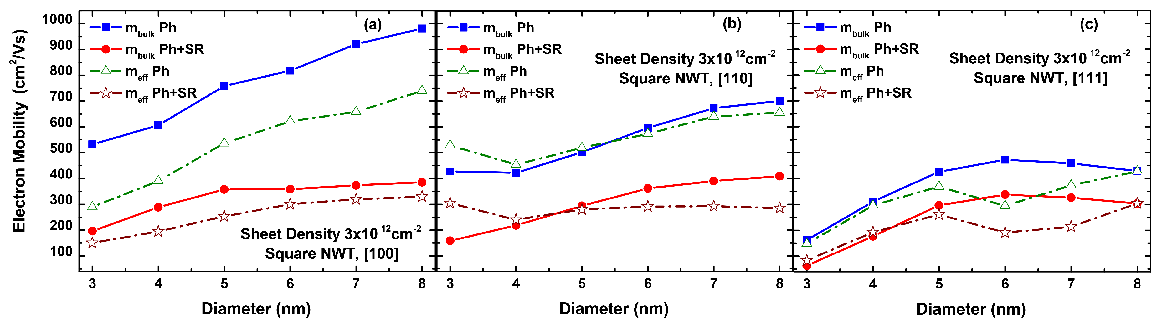
4.2. Mobility: A Kubo-Greenwood Study

The aim of this section is to present a simulation study of the impact of the effective masses on the electron mobility in silicon nanowires as a function of their diameter and orientation, comparing the use of the bulk (m b u l k ) and the calibrated (m e f f ) effective masses. For this purpose, we chose a square shape NWT with an equivalent oxide thickness (EOT) of 0.8 nm and diameters ranging from 3 to 8 nm to describe the electronic behavior from a device with strong confinement impact (3 nm) to a near bulk-like device (8 nm) [18]. We studied the following intrinsic mobility limiting mechanisms: (i) acoustic phonon scattering, with acoustic deformation potential 12 eV; (ii) optical phonon scattering, with the fixed parameters for the different branches defined in Table 5; and (iii) surface roughness scattering, with root mean square ( Δ R M S ) and correlation length 0.48 and 1.3 nm, respectively. In particular, we report the mobility for the total phonon (Ph) and the combined total phonon and surface roughness (Ph+SR) scattering effects with a sheet density of 3 × 10 12 cm 2 .
Figure 3 shows the Ph and Ph+SR electron mobilities considering both m b u l k and the calibrated m e f f , which values are taken from Table 1, for different channel orientations: (a) [100]; (b) [110]; and (c) [111]. In general, as the transport effective masses were introduced in the scattering rate equations [12], their modification directly altered the mobility. Due to the relaxation time approach, the mobility for a particular scattering mechanism was inversely proportional to its rate and thus to the transport effective mass. As expected in Figure 3, the inclusion of SR significantly reduced the mobility because it dominated for very high sheet concentrations. Moreover, the lowest mobility was [111] devices due to the lower valley splitting energy and higher transport masses [11].
Then, different results can be highlighted when m e f f was included for the different channel orientations. First, the electron’s Ph limited mobility was reduced in the [100] orientation due to the higher m e f f in comparison to m b u l k for the dominant valley ( Δ y ) [19]. This reduction was caused when m e f f was considered instead of m b u l k , which was less pronounced when SR was introduced in the total mobility (Ph+SR), because this mechanism mainly depended on the electrostatic force normal to the Si-SiO 2 interface. Second, two scenarios could be distinguished as a function of the diameter in the [110] orientation for both Ph and Ph+SR cases. On the one hand, the electron mobility increased when m e f f was taken into account for the devices with the smallest cross-sections (3 and 4 nm devices). The reason was similar but opposite compared to the one for the [100] orientation: the lower transport m e f f in comparison to m b u l k for the dominant valley ( Δ z ) reduced the scattering rate and, thus, enhanced the mobility. On the other hand, for square nanowires with diameter bigger than 5 nm, this difference was significantly reduced and thus the influence of the other valleys, which presented higher m e f f , had more importance. Third, there was a mismatch in the transport m e f f tendency between 5 and 6 nm devices for the [111] orientation (as shown in Table 1). Accordingly, even though the impact of m e f f was quite low for smaller devices in this orientation, the mobility for both Ph and Ph+SR cases decreased following the aforementioned tendency for diameters higher than 6 nm.

4.3. Ballistic Transfer Characteristic: A NEGF Study

Figure 4 shows the transfer characteristic of a square NWT having a cross-sectional area of 9 nm 2 and gate length of 10 nm. The simulations were performed in a ballistic transport approximation, as, for smaller channel lengths, the scaling was expected to play a relatively smaller role [10]. The comparison showed that the on-current could be significantly different if calibrated effective masses were used instead of the bulk masses. In this particular case, the drain current was reduced if calibrated effective masses were used rather than the bulk ones. This was because transport effective masses for the Δ valleys were more than their bulk counterparts and hence resulted in a reduction of the current.

5. Conclusions

In this study, we developed a systematic methodology to extract the effective masses of a nanostructure from their electronic band structure. We employed our method to compile the effective masses for technologically relevant dimensions and cross-section shapes for silicon nanowires achieving a good agreement with their tight binding counterparts. This makes the tabulated effective masses presented in this paper valuable to the entire microelectronic community. We also performed a comprehensive mobility study for a square nanowire with different crystallographic orientations and cross-sectional areas, which emphasized the importance of using correct effective masses. The importance of the calibrated effective mass was also corroborated by performing a full transfer characteristic simulation using ballistic NEGF.

Author Contributions

Writing—original draft preparation, O.B. and C.M.-B.; methodology, (Effective Mass extraction) O.B. and J.L., (mobility simulations and bulk effective masses) C.M.-B., and (NEGF simulations) S.B.; writing—review and editing, H.C.-N., and V.G.; and supervision, V.G. and A.A.

Funding

The work is supported by Horizon2020 European Project: REMINDER/687931, (http://www.reminder2020.eu).

Conflicts of Interest

The authors declare no conflict of interest.

References

  1. Dennard, R.H.; Gaensslen, F.H.; Rideout, V.L.; Bassous, E.; LeBlanc, A.R. Design of ion-implanted MOSFET’s with very small physical dimensions. IEEE J. Solid-State Circuits 1974, 9, 256–268. [Google Scholar] [CrossRef]
  2. Moore, G.E. Cramming more components onto integrated circuits, Reprinted from Electronics, volume 38, number 8, April 19, 1965, pp.114 ff. IEEE Solid-State Circuits Soc. Newsl. 2006, 11, 33–35. [Google Scholar] [CrossRef]
  3. Badami, O.; Lizzit, D.; Driussi, F.; Palestri, P.; Esseni, D. Benchmarking of 3-D MOSFET Architectures: Focus on the Impact of Surface Roughness and Self-Heating. IEEE Trans. Electron Devices 2018, 65, 3646–3653. [Google Scholar] [CrossRef]
  4. Dupre, C.; Hubert, A.; Becu, S.; Jublot, M.; Maffini-Alvaro, V.; Vizioz, C.; Aussenac, F.; Arvet, C.; Barnola, S.; Hartmann, J.; et al. 15nm-diameter 3D stacked nanowires with independent gates operation: ϕFET. In Proceedings of the 2008 IEEE International Electron Devices Meeting, San Francisco, CA, USA, 15–17 December 2008; pp. 1–4. [Google Scholar] [CrossRef]
  5. Colinge, J.P. Multiple-gate SOI MOSFETs. Solid-State Electron. 2004, 48, 897–905. [Google Scholar] [CrossRef]
  6. Song, Y.; Xu, Q.; Luo, J.; Zhou, H.; Niu, J.; Liang, Q.; Zhao, C. Performance Breakthrough in Gate-All-Around Nanowire n- and p-Type MOSFETs Fabricated on Bulk Silicon Substrate. IEEE Trans. Electron Devices 2012, 59, 1885–1890. [Google Scholar] [CrossRef]
  7. Luisier, M.; Schenk, A.; Fichtner, W.; Klimeck, G. Atomistic simulation of nanowires in the sp3d5s* tight-binding formalism: From boundary conditions to strain calculations. Phys. Rev. B 2006, 74, 205323. [Google Scholar] [CrossRef]
  8. Neophytou, N.; Kosina, H. Large thermoelectric power factor in p-type Si (110)/[110] ultra-thin-layers compared to differently oriented channels. J. Appl. Phys. 2012, 112, 024305. [Google Scholar] [CrossRef] [Green Version]
  9. Van der Steen, J.P.J.; Esseni, D.; Palestri, P.; Selmi, L.; Hueting, R.J.E. Validity of the Parabolic Effective Mass Approximation in Silicon and Germanium n-MOSFETs With Different Crystal Orientations. IEEE Trans. Electron Devices 2007, 54, 1843–1851. [Google Scholar] [CrossRef] [Green Version]
  10. Berrada, S.; Dutta, T.; Carrillo-Nunez, H.; Duan, M.; Adamu-Lema, F.; Lee, J.; Georgiev, V.; Medina-Bailon, C.; Asenov, A. NESS: New flexible Nano-Electronic Simulation Software. In Proceedings of the 2018 International Conference on Simulation of Semiconductor Processes and Devices (SISPAD), Austin, TX, USA, 24–26 September 2018; pp. 22–25. [Google Scholar] [CrossRef]
  11. Neophytou, N.; Kosina, H. Atomistic simulations of low-field mobility in Si nanowires: Influence of confinement and orientation. Phys. Rev. B 2011, 84, 085313–085328. [Google Scholar] [CrossRef]
  12. Sadi, T.; Medina-Bailon, C.; Nedjalkov, M.; Lee, J.; Badami, O.; Berrada, S.; Carrillo-Nuñez, H.; Georgiev, V.; Selberherr, S.; Asenov, A. Simulation of the Impact of Ionized Impurity Scattering on the Total Mobility in Si Nanowire Transistors. Materials 2019, 12, 124. [Google Scholar] [CrossRef] [PubMed]
  13. Esseni, D.; Palestri, P.; Selmi, L. Nanoscale MOS Transistors - Semi-Classical Transport and Applications, 1st ed.; Cambridge University Press: Cambridge, UK, 2011. [Google Scholar]
  14. QuantumATK version O-2018.06. 2018. Available online: https://www.synopsys.com/silicon/quantumatk/ (accessed on 19 April 2019).
  15. Boykin, T.B.; Klimeck, G.; Oyafuso, F. Valence band effective-mass expressions in the sp3d5s* empirical tight-binding model applied to a Si and Ge parametrization. Phys. Rev. B 2004, 69, 115201. [Google Scholar] [CrossRef]
  16. Rahman, A.; Lundstrom, M.S.; Ghosh, A.W. Generalized effective-mass approach for n-type metal-oxide-semiconductor field-effect transistors on arbitrarily oriented wafers. J. Appl. Phys. 2005, 97, 053702. [Google Scholar] [CrossRef]
  17. Bescond, M.; Cavassilas, N.; Lannoo, M. Effective-mass approach for n-type semiconductor nanowire MOSFETs arbitrarily oriented. Nanotechnology 2007, 18, 255201. [Google Scholar] [CrossRef]
  18. Stanojević, Z.; Baumgartner, O.; Sverdlov, V.; Kosina, H. Electronic band structure modeling in strained Si-nanowires: Two band k·p versus tight binding. In Proceedings of the International Workshop on Computational Electronis (IWCE), Pisa, Italy, 26–29 October 2010; pp. 1–4. [Google Scholar] [CrossRef]
  19. Medina-Bailon, C.; Sadi, T.; Nedjalkov, M.; Lee, J.; Berrada, S.; Carrillo-Nuñez, H.; Georgiev, V.; Selberherr, S.; Asenov, A. Impact of the Effective Mass on the Mobility in Si Nanowire Transistors. In Proceedings of the 2018 International Conference on Simulation of Semiconductor Processes and Devices (SISPAD), Austin, TX, USA, 24–26 September 2018; pp. 297–300. [Google Scholar] [CrossRef]
Figure 1. (a) Flowchart of the simulator NESS including the modules herein used. (b) Schematic of a simulated nanowire device along with the doubly-degenerate Δ valleys used in the simulations.
Applsci 09 01895 g001
Figure 2. Comparison of the electronic band structure calculated within the parabolic effective mass approximation and tight binding method for nanowires oriented along: (a) [100] direction; (b) [110] direction; and (c) [111] direction. Good agreement in terms of the subband minima and curvature at the minima are obtained for all the three orientations.
Applsci 09 01895 g002
Figure 3. Electron mobility as a function of the diameter for a square nanowire with m b u l k and m e f f masses and a sheet density of 3 × 10 12 cm 2 , considering: (a) [100] channel orientation; (b) [110] channel orientation; and (c) [111] channel orientation. The total phonon (Ph) and the combined total phonon and surface roughness (Ph+SR) scattering effects are considered.
Applsci 09 01895 g003
Figure 4. Comparison of the transfer characteristics calculated using the calibrated and bulk effective mass.
Applsci 09 01895 g004
Table 1. Effective masses for square nanowire.
Square [100]Square [110]Square [111]
Side [nm]Valleym y [m0]m z [m0]m x [m0]m y [m0]m z [m0]m x [m0]m y [m0]m z [m0]m x [m0]
3 Δ x 0.2790.2790.9470.5050.2520.5780.7820.2410.447
Δ y 1.0080.2620.2660.4980.2510.5780.7940.2360.447
Δ z 0.2530.9830.2660.3250.8160.1720.2480.6700.447
4 Δ x 0.2450.2450.9210.4440.2330.5540.4910.2590.434
Δ y 0.9860.2290.2440.4250.2360.5540.4940.2540.434
Δ z 0.2300.9220.2440.4250.9340.1830.2640.4470.434
5 Δ x 0.2290.2290.9110.4330.2240.5620.4540.2380.430
Δ y 0.9510.2190.2310.4260.2250.5620.4120.2420.430
Δ z 0.2190.8940.2310.2600.9080.1900.2440.4070.430
6 Δ x 0.2460.2460.9050.3940.2450.5610.4580.2820.478
Δ y 0.9670.2530.2220.3930.2450.5610.4220.2940.478
Δ z 0.2530.9290.2220.2740.9300.1930.4250.2920.478
7 Δ x 0.2380.2380.9020.3740.2110.5570.4430.2290.435
Δ y 0.9470.2560.2170.3740.2110.5570.3990.2430.435
Δ z 0.2560.9010.2170.2300.8820.1950.2380.4020.435
8 Δ x 0.2090.2090.8960.3620.2070.5890.4310.2190.433
Δ y 0.8960.2120.2120.3620.2070.5890.3850.2340.433
Δ z 0.2020.8780.2120.2130.8940.1970.2280.3870.433
Table 2. Effective masses for circular nanowire.
Circle [100]Circle [110]Circle [111]
Diameter [nm]Valleym y [m0]m z [m0]m x [m0]m y [m0]m z [m0]m x [m0]m y [m0]m z [m0]m x [m0]
3 Δ x 0.2540.2540.9420.5490.2070.6010.9700.1950.476
Δ y 0.8360.2500.2730.5470.2010.6010.9640.1920.476
Δ z 0.2370.8750.2730.2990.7560.1500.1920.9620.476
4 Δ x 0.2390.2390.9100.4430.2100.5740.6020.2160.445
Δ y 0.9300.2230.2500.4460.2010.5740.6050.2150.445
Δ z 0.2250.8970.2500.2480.9100.1750.2160.6030.445
5 Δ x 0.2270.2270.9100.4290.2150.5580.4580.2300.447
Δ y 0.8940.2220.2350.4390.2070.5580.4580.2300.447
Δ z 0.2180.8860.2350.2390.9870.1840.2290.4500.447
6 Δ x 0.2210.2210.9070.3810.2070.5630.4430.2270.433
Δ y 0.8800.2160.2260.3840.2030.5630.4490.2230.433
Δ z 0.2160.8790.2260.2280.8690.1890.2230.4420.433
7 Δ x 0.2290.2290.9010.3720.2090.5600.4400.2240.434
Δ y 0.8270.2490.2190.3740.2060.5600.4410.2210.434
Δ z 0.2460.8370.2190.2260.8940.1920.2210.4370.434
8 Δ x 0.2330.2330.8960.3640.2060.5670.4310.2160.436
Δ y 0.8090.2630.2140.3630.2060.5670.4310.2160.436
Δ z 0.2620.7970.2140.2220.8910.1940.2200.4270.436
Table 3. Effective masses for elliptical nanowire having major and minor diameter as “a” and “’b”, respectively.
Ellipse [100]Ellipse [110]Ellipse [111]
a [nm]b [nm]Valleym y [m0]m z [m0]m x [m0]m y [m0]m z [m0]m x [m0]m y [m0]m z [m0]m x [m0]
32.00 Δ x 0.3830.2380.9860.4690.2510.5740.9720.2920.570
Δ y 0.2051.0720.2830.5700.2090.5741.0050.2840.570
Δ z 0.6830.2870.2830.1831.2900.1350.7670.2940.570
42.67 Δ x 0.3420.1890.9350.5530.2010.6290.6670.2450.467
Δ y 0.1990.9160.2540.4890.2070.6290.6740.2420.467
Δ z 0.8870.2100.2540.2131.1490.1600.5930.2320.467
53.33 Δ x 0.3000.1930.9150.4520.2050.5600.3890.3010.449
Δ y 0.2030.8800.2380.4720.1950.5600.3950.2950.449
Δ z 0.8160.2180.2380.2410.7970.1830.4190.2550.449
64.00 Δ x 0.2740.1990.9120.3910.2180.5630.3440.3190.455
Δ y 0.2070.8950.2280.4090.2050.5630.3380.3220.455
Δ z 0.8920.2140.2280.2180.9170.1880.3960.2590.455
74.67 Δ x 0.2610.2000.9060.4090.2070.5650.3310.3220.438
Δ y 0.2100.8790.2200.4050.2040.5650.3200.3270.438
Δ z 0.8960.2120.2200.2240.8820.1920.3890.2540.438
85.33 Δ x 0.2430.2020.9030.3700.2080.5480.3270.3310.444
Δ y 0.2070.8780.2150.3730.2010.5480.3120.3380.444
Δ z 0.8750.2080.2150.2080.8850.1930.3940.2480.444
Table 4. Effective masses for Bulk silicon along different crystallographic directions.
Bulk [100]Bulk [110]Bulk [111]
Valleym y [m0]m z [m0]m x [m0]m y [m0]m z [m0]m x [m0]m y [m0]m z [m0]m x [m0]
Δ x 0.2010.2010.8910.3280.2010.5460.4310.2010.431
Δ y 0.8910.2010.2010.3280.2010.5460.4310.2010.431
Δ z 0.2010.8910.2010.2010.8910.2010.4310.2010.431
Table 5. Deformation potential (D O P ) and energy considered for the different branches in the optical scattering mechanism.
Optical Phonon TypeD OP (eV/m)Energy (eV)
g-type, TA 5 × 10 9 0.01206
g-type, LA 8 × 10 9 0.01853
g-type, LO 3 × 10 10 0.063
f-type, TA 1.5 × 10 9 0.01896
f-type, LA 3.4 × 10 9 0.0474
f-type, TO 4 × 10 10 0.059

