Comparison of Various Factors Affected TID Tolerance in FinFET and Nanowire FET


Department of Electronic Engineering Korea National, University of Transportation, Chungju-si 27469, Korea
*
Author to whom correspondence should be addressed.
†
Those authors contributed equally to this work.
Appl. Sci. 2019, 9(15), 3163; https://doi.org/10.3390/app9153163
Submission received: 29 June 2019
/
Revised: 26 July 2019
/
Accepted: 29 July 2019
/
Published: 3 August 2019
(This article belongs to the Special Issue Silicon Nanowires and Their Applications)
Abstract
:Analysis of the radiation effects in a device is of great importance. The gate all around (GAA) structure that contributes to device scaling not only solves the short channel effects (SCE) problem but also makes the device more resistant in radiation environments. In this article, the total ionizing dose (TID) simulation of nanowire FET (NW) and FinFET was performed. Both these devices were compared and analyzed in terms of the shift of threshold voltage (VT). The channel insulator was composed of two materials, SiO2 and HfO2. To improve the accuracy of the simulation, the interfacial trap parameter of SiO2 and HfO2 was applied. Based on the simulation result, the NW with a larger oxide area and larger gate controllability showed less VT shift than that of the FinFET. It was therefore proved that NW had better TID resistance characteristics in a radiation environment. The gate controllability was found to affect the TID effect more than the oxide area. In addition, we analyzed the manner in which the TID effect changed depending on the VDD and channel doping.
1. Introduction
The effects of the total ionizing dose (TID) on electronic devices are critical issues in various fields such as space and nuclear applications. To reduce the radiation effects on the electronic components, three radiation hardening methods have been widely considered: radiation hardening by process (RHBP), radiation hardening by shielding (RHBS), and radiation hardening by design (RHBD) [1,2,3,4]. The international thermonuclear experimental reactor (ITER) studies the TID effect for the development of a precise remote control system [5]. Electronic equipment operating in a radiation environment is subject to radiations that lead to defects in transistors. The TID effects, single event effects (SEEs), and displacement damage (DD) can lead to disturbances in the reliable operation of semiconductor devices due to radiation [6,7,8,9,10]. In particular, in the TID effect, the trapped holes in the oxide of transistor in the electron hole pairs (EHP) are caused by radiation and change in the threshold voltage (VT) [11]. The hole trapped in the oxide results in the inversion charge of the channel region and leads to change in VT. In particular, nanoscale devices can affect other static and dynamic parameters [12]. Therefore, the reliability of the device is degraded. The devices with a 3D gate structure can solve the SCE problem and enable continuous scaling [13,14,15]. In particular, FinFET, which has a tri-gate structure, and NW, which has a gate all around (GAA) structure, are being studied as effective solutions for device miniaturization [16]. Therefore, both structures devices must be studied for mitigating the radiation effects. In this paper, the TID simulation of NW and FinFET was used to analyze that received more of the TID effect, depending on the structural part of the device. The experiments were performed considering the oxide area and gate controllability, which are the structural elements affected by the TID effect. For a more accurate comparison, the TID simulation was performed by calibrating the size and current level of the NW and FinFET. Through these experiments, compared to the FinFET, we observed that the VT of the NW changed insignificantly and that this device was more resistant in the radiation environment. This result shows that gate controllability is more effective for causing radiation tolerance than the oxide area. However, the oxide area of the hole trap is a key factor in the TID effect. As the oxide area increases, the number of trapped holes also increases and consequently, the reliability of the device is further degraded. However, by introducing the GAA structure, the gate controllability can be improved to suppressing the TID effect in the oxide area. In addition, the TID characteristics were confirmed by changing the VDD and channel doping, which affect the resistance to the TID effect. Therefore, the importance of improving gate controllability, which is a method of suppressing the TID effect, is herein presented.
2. Simulation Methodology
2.1. Design Structure for TID Simulation
Prior to the simulation, the NW was stacked in five stages to match the current level and device size. Table 1 presents the basic physical device parameters used in this study. With the use of a 3D technology computer-aided design (TCAD) simulation tool, the FinFET and 5ch-NW were similarly constructed (Table 1). Tfin is the FinFET width, Dnw is the 5ch-NW diameter, Lg is the channel length, Hfin is the FinFET height, and Hnw is the 5ch-NW’s total height. In addition, the FinFET was manufactured by referring to the International Technology Roadmap for Semi-conductors (ITRS) [17]. Figure 1 shows the TCAD structure of the FinFET and 5ch-NW.
The electrodes of the devices were made of tungsten, the body of silicon, the p-type doping was boron, and the n-type doping was phosphorus. The devices placed SiO2 (0.5 nm, k = 3.9) and HfO2 (2 nm, k = 25) on the FinFET and 5ch-NW channel insulator material. The equivalent oxide thickness (EOT) can be calculated using Equation (1).
The electrical properties were also calibrated for a fair comparison of the TID effects. Figure 2 shows the ID-VG characteristics with the FinFET and 5ch-NW and demonstrates that the electrical characteristics of FinFET and 5ch-NW were calibrated.
2.2. TID Simulation of Various Factors
The TID simulation used the Silvaco victory device software [18]. The Klaassen model used in the simulation reflects various parameters such as electron and hole mobility, trap parameters, and recombination parameters [19,20,21,22,23]. The trap-detrap model parameters in the oxide region by radiation were used in the same way as in [24]. For a more precise simulation, the interfacial trap coefficient between SiO2 and HfO2 was calculated by introducing an interfacial trap parameter between the insulators. We generated the corresponding ID-VG curves by applying the TID effect. The radiation source was a γ-ray irradiation performed using a Co60 source [25]. Radiation was irradiated 1 rad/s for the devices. The input VDD was equal to 0.65 V and the sweep VG was in the range 0–0.7 V for the electrical characteristics of 100 Krad, 1 Mrad, 10 Mrad, and 100 Mrad. The simulation confirmed the TID effect on the structural aspects of the FinFET and 5ch-NW. All comparative calculations were performed with the same efficiency as the charge capture [9].
To observe VDD influence, the VDD was simulated by varying it from 0.65 V to 0.1 V. The VT shift amount was compared based on the VDD in the TID simulation. We applied the VDD conditions mentioned above to FinFET and 5ch-NW, and the VG sweep was done in the same way from 0 V to 0.7 V.
The TID characteristics of the two aforementioned devices according to the changed channel doping concentration were confirmed as the channel doping concentration changed. The TID effect change was confirmed by the VT shift. The channel doping concentration was changed from 1 × 1016 cm−3 to 1 × 1018 cm−3. After changing the channel doping of both the devices, the initial simulation without radiation was compared to the simulation with TID of 10 Mrad.
3. Results and Discussion
Figure 3 shows the basic structure of the FinFET and 5ch-NW as well as the interface hole trap after TID simulation. Figure 3a,b show that the physical thickness and EOT of the insulator were the same. Figure 3c,d show the interface hole traps of the FinFET and 5ch-NW, respectively. The hole traps at the interface between SiO2 and HfO2 was confirmed to improve simulation accuracy. Figure 3c,d also show that the hole-trapped interface between Si and SiO2.
TID is a phenomenon generated because of the accumulation of radiation irradiated to the device. When the radiation penetrates through the insulator region of a device, EHP is generated through the ionization process. Due to their difference in mobility, the generated electrons rapidly diffuse out from the dielectric region. However, some holes are captured in the insulator region trap sites, thereby increasing the leakage current and causing a negative VT shift [26,27].
Figure 4 illustrates the TID simulation method. In Figure 4a, VG according to the transient time takes the shape of a pulse. The ID-VG curve changes depending on if the pulse is rise or down. In this figure, we can see the upsweep when the purse is rising. Additionally, we can see the downsweep when the purse is going down. The width of the pulse is related to the amount of dose. We can see the simulation results when the pulse is end. The results show the VT shift and that means the hole is trapped in the interface.
Figure 5 shows the electrical characteristics of the device with the TID effects for each radiation level. We extracted the VT when the drain current was 1 × 10⁻⁷ [A] using the current constant method in Figure 5. It shows that the VT shifted because the holes generated by the radiation were trapped in the insulator. Therefore, the shift tendency increases with the increase in the TID. In Figure 5, relatively low levels of radiation did not affect the transfer characteristics. Due to the nanoscale oxide area, the hole trap caused by the radiation was reduced. Additionally, the GAA structure increased the gate holding power and reduced the effect of the trapped charge.
Figure 5c,d show the log scale of ID-VG where the off current increase phenomenon, caused by the TID effects, was confirmed. In the figure, we can see that the off current change of 5ch-NW was less than that of FinFET. This shows that the effect of suppressing the SCE also suppressed the TID effects. Table 2 presents the VT value for each TID amount of both the FinFET and 5ch-NW.
Figure 5e,f show the transconductance of the FinFET and 5ch-NW. It can be noticed that the transconductance increases with radiation, as shown in Figure 5e,f, because of the decrease of VT and the flow of more drain current at the same gate voltage.
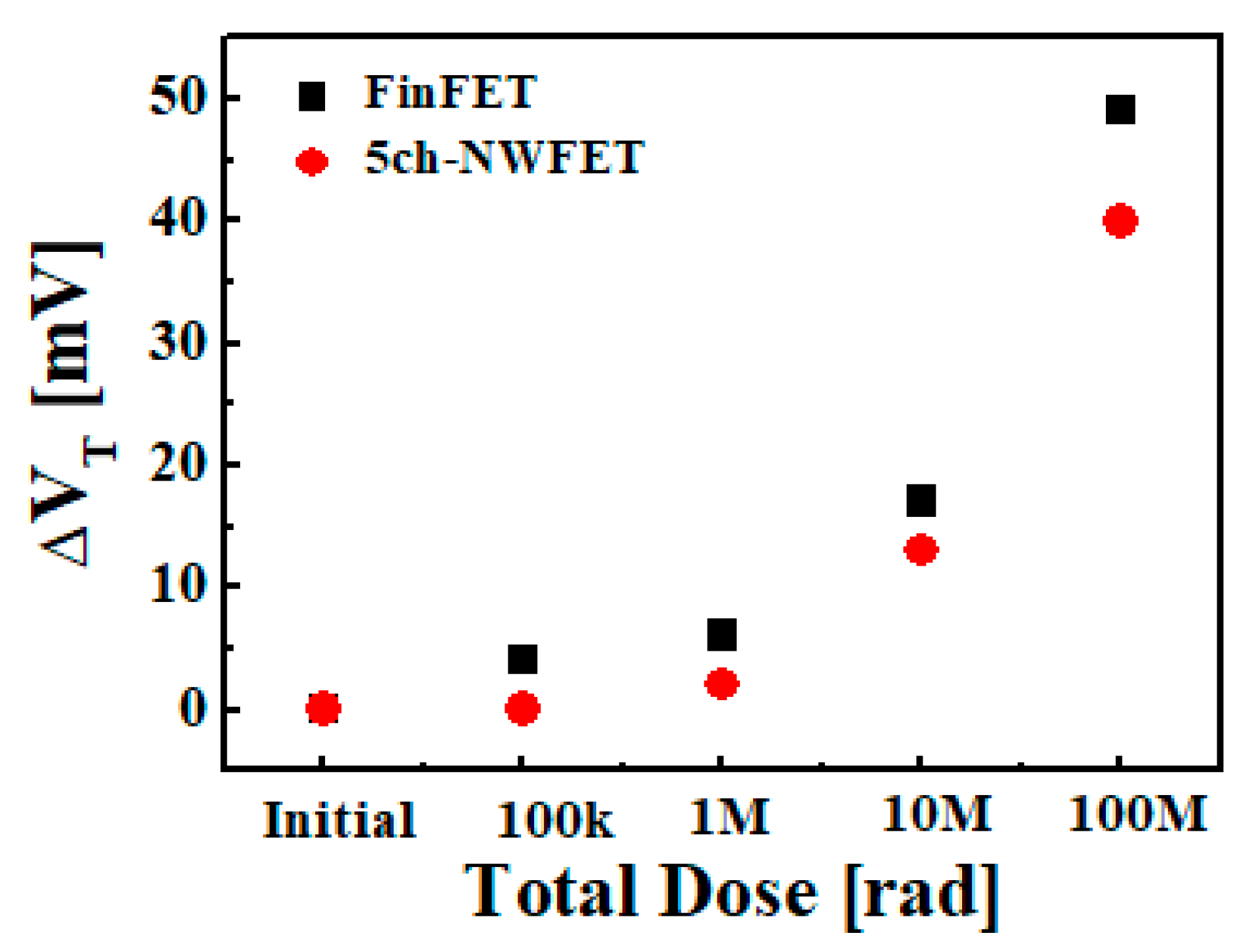
Figure 6 shows the details the VT shift for each device. In the case of FinFET, a 48 mV shift from 100 Mrad than the initial was observed. In the case of the 5ch-NW, roughly 42 mV shift from 100 Mrad than the initial was observed. The 5ch-NW therefore showed less VT shifts than the FinFET, as per the simulation results.
The 5ch-NW had a larger oxide area than the FinFET. Therefore, it was reflected to have a greater TID effect and a larger VT shift. However, these were less in the case of the 5ch-NW because of superior gate controllability. The GAA structure improved the gate controllability because all the sides are covered with the gate. This does not only address SCE, but also improves tolerance to the TID effect [28]. Structurally, the oxide area of 5ch-NW was approximately 96.1 nm2, which is larger than that in FinFET. However, the TID effect in 5ch-NW was less than that in FinFET in the above-mentioned experiment. Therefore, it shows that the gate controllability factor is more crucial than the oxide area in TID effect suppression.
Figure 7 depicts a graph of the TID simulation result with VDD set at 0.1 V and 0.65 V. In Figure 7c, at higher radiation, the VT shifts significantly than in the case of lower radiation because of the hole traps in the FinFET and 5ch-NW. Additionally, because of the strong TID effect, the FinFET and 5ch-NW are less affected by VDD at the higher radiation. However, the FinFET is affected by VDD when low radiation is applied, because the gate controllability of the FinFET is weaker than that of the 5ch-NW. Therefore, the 5ch-NW is not significantly affected by VDD.
Table 3 lists the VT shift according to the variation of VDD. In the case of 5ch-NW, there was almost no change owing to its better gate controllability, which reduced the VDD influence.
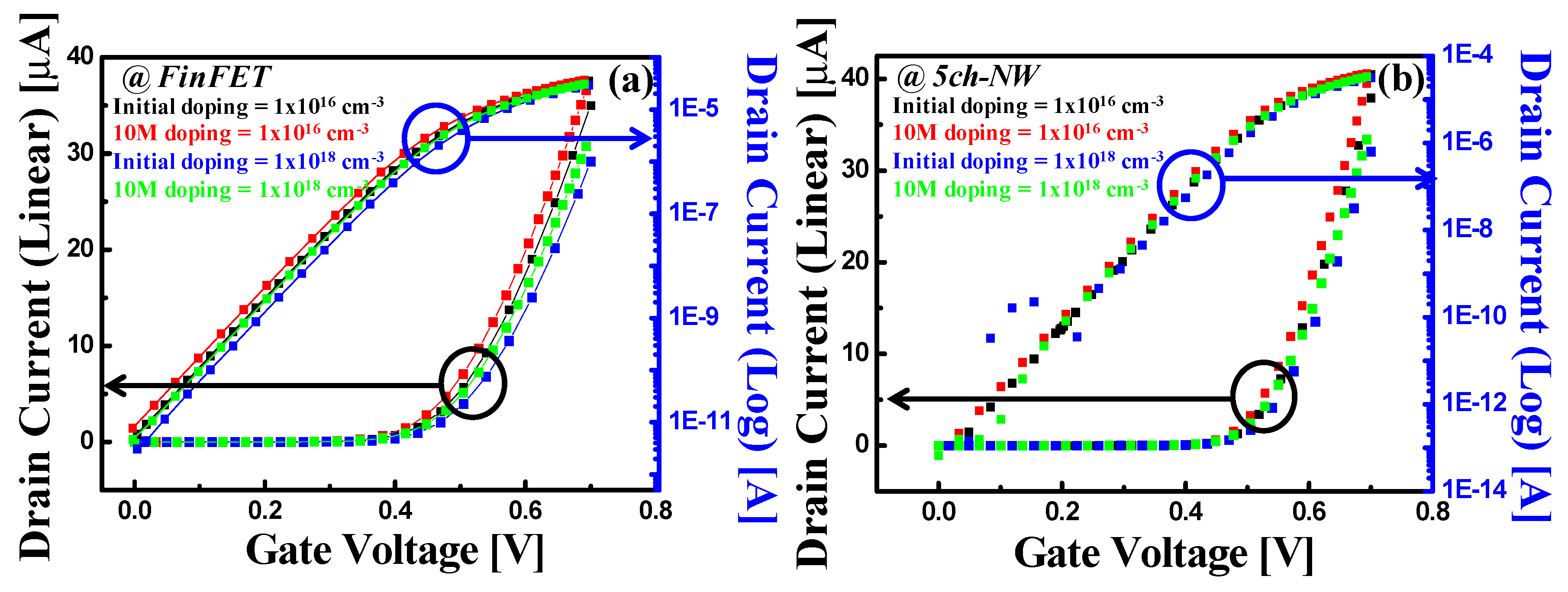
Figure 8 shows that the ID-VG changed due to the TID effect. Figure 8a shows the ID-VG of the FinFET, and Figure 8b shows the ID-VG of the 5ch-NW. We can see that the VT changed and how it was different if the channel doping was changed. First, the VT decreased due to the TID effect, and the VT decreased on the same way when the channel doping was changed. In the case of channel doping at 1 × 1016 cm−3, it was confirmed that the VT variation due to the TID effect was similar to the VT variation at 1 × 1018 cm−3. Therefore, the VT increased when the channel doping increased in both the FinFET and 5ch-NW, and the VT decreased due to the TID effect at both 1 × 1016 cm−3 and 1 × 1018 cm−3.
Table 4 lists the VT variation based on channel doping. The doping of the FinFET changed from 1 × 1016 cm−3 to 1 × 1018 cm−3, and that of the 5ch-NW was also changed in a similar way. Increasing channel doping in FinFET and 5ch-NW caused an increase in the initial VT. In addition, when radiation was applied, the VT and the TID effect decreased for all cases, regardless of doping. When the doping was changed to 1 × 1018 cm−3, the change in VT was less in the 5ch-NW than that in the FinFET as less of the interface and oxide traps were generated in the case of the former [29]. As channel doping increased, 10 M radiation appears to have significantly reduce VT, however, this can only attributed to the increase in the absolute value of the initial amount. In fact, very silght difference was observed when calculating the percentage variation of the aforementioned amount. As presented in Table 4, the VT variation percentage was found to be similar between the channel doping of 1 × 1016 cm−3 and 1 × 1018 cm−3 for both the FinFET and 5ch-NW. Thus, channel doping had little or no influence on the TID effect in the FinFET and 5ch-NW.
4. Conclusions
In this paper, we found that the 5ch-NW GAA devices exhibited less ionizing radiation sensitivity when compared to the FinFET device. Structurally, the 5ch-NW device had an oxide area of approximately 96.1 nm2, which is larger than that of the FinFET. However, in our experiment, the TID effect of 5ch-NW was observed to be less than that of the FinFET. It was shown that the gate controllability factor is more crucial to the suppression of the TID effect than the oxide area. The GAA structure, which has larger gate controllability, confirmed that the TID effect problem can be effectively resolved. The GAA structure and high-k dielectric materials have to be introduced to improve gate controllability. Furthermore, the 5ch-NW was not found to be affected by VDD. However, the FinFET was affected by VDD when low radiation was applied. Therefore, devices with strong gate controllability were not affected by TID and channel doping had little or no influence on the TID effect.
Author Contributions
H.W. simulation and analysis of data and Methodology; I.H. correcting article and design figures; Y.J. writing review and editing; M.K. project administration and supervision and proofreading the manuscript and funding.
Funding
This research was supported by the Basic Science Research Program through the National Research Foundation of Korea (NRF) funded by the Ministry of Education (2018R1A6A1A03023788), the Korea Institute for Advancement of Technology (KIAT) grant funded by the Korea Government (MOTIE) (N000P00008500, The Competency Development Program for Industry Specialist), the National R&D Program through the National Research Foundation of Korea (NRF) funded by the Ministry of Science, ICT, and Future Planning (2017M1A7A1A01016265). This research was also supported by the MOTIE (Ministry of Trade, Industry & Energy (10085645) and KSRC (Korea Semiconductor Research Consortium) support program for the development of future semiconductor devices.
Conflicts of Interest
The authors declare no conflict of interest.
References
- Leroux, P.; Van Koeckhoven, W.; Verbeeck, J.; Van Uffelen, M.; Esqué, S.; Ranz, R.; Damiani, C.; Hamilton, D. Design of a MGy radiation tolerant resolver-to-digital convertor IC for remotely operated maintenance in harsh environments. Fusion Eng. Des. 2014, 89, 2314–2319. [Google Scholar] [CrossRef]
- Haddad, N.F.; Kelly, A.T.; Lawrence, R.K.; Li, B.; Rodgers, J.C.; Ross, J.F.; Warren, K.M.; Weller, R.A.; Mendenhall, M.H.; Reed, R.A. Incremental enhancement of SEU hardened 90 nm CMOS memory cell. IEEE Trans. Nucl. Sci. 2011, 58, 975–980. [Google Scholar] [CrossRef]
- Clark, L.T.; Mohr, K.C.; Holbert, K.E.; Yao, X.; Knudsen, J.; Shah, H. Optimizing radiation hard by design SRAM cells. IEEE Trans. Nucl. Sci. 2007, 54, 2028–2036. [Google Scholar] [CrossRef]
- Gatti, U.; Calligaro, C.; Pikhay, E.; Roizin, Y. Radiation-hardened techniques for CMOS flash ADC. In Proceedings of the IEEE International Conference on Electronics Circuits and Systems (ICECS), Marseille, France, 7–10 December 2014; pp. 1–4. [Google Scholar]
- Verbeeck, J.; Cao, Y.; Van Uffelen, M.; Casellas, L.M.; Damiani, C.; Morales, E.R.; Santana, R.R.; Meek, R.; Hais, B.; Hamilton, D.; et al. Qualification method for a 1 MGy-tolerant front-end chip designed in 65 nm CMOS for the read-out of remotely operated sensors and actuators during maintenance in ITER. Fusion Eng. Des. 2015, 96–97, 1002–1005. [Google Scholar] [CrossRef]
- Verbeeck, J.; Van Uffelen, M.; Steyaert, M.; Leroux, P. 17 bit 4.35 mW 1 kHz delta sigma ADC and 256-to-1 multiplexer for remote handling instrumentation equipment. Fusion Eng. Des. 2013, 88, 1942–1946. [Google Scholar] [CrossRef]
- Cao, Y.; Cock, W.D.; Steyaert, M.; Leroux, P. A 4.5 MGy TID-tolerant CMOS bandgap reference circuit using a dynamic base leakage compensation technique. IEEE Trans. Nucl. Sci. 2013, 60, 2819–2824. [Google Scholar] [CrossRef]
- Virmontois, C.; Goiffon, V.; Magnan, P.; Girard, S.; Inguimbert, C.; Petit, S.; Rolland, G.; Saint-Pé, O. Displacement damage effects due to neutron and proton irradiations on CMOS image sensors manufactured in deep submicron technology. IEEE Trans. Nucl. Sci. 2010, 57, 3101–3108. [Google Scholar] [CrossRef]
- Barnaby, H.J. Total-ionizing-dose effects in modern CMOS technologies. IEEE Trans. Nucl. Sci. 2006, 53, 3103–3121. [Google Scholar] [CrossRef]
- Martin, H.; Martin-Holgado, P.; Morilla, Y.; Entrena, L.; San-Millan, E. Total ionizing dose effects on a delay-based physical unclonable function implemented in FPGAs. Electronics 2018, 7, 163. [Google Scholar] [CrossRef]
- Seo, D.; Trang, L.D.; Han, J.W.; Kim, J.; Lee, S.; Chang, I.J. Total Ionizing Dose Effect on Ring Oscillator Frequency in 28nm FD-SOI Technology. IEEE Electron. Device Lett. 2018, 39, 1728–1731. [Google Scholar] [CrossRef]
- Zebrev, G. Static and Dynamic Oxide-Trapped-Charge-Induced Variability in Nanoscale CMOS Circuits. IEEE Trans. Electron Devices 2019, 66, 2483–2488. [Google Scholar] [CrossRef]
- Zhai, Y.; Mathew, L.; Rao, R.; Palard, M.; Chopra, J.S.; Ekerdt, G.; Register, L.F.; Banerjee, S.K. High-Performance Vertical Gate-All-Around Silicon Nanowire FET with High-k/Metal Gate. IEEE Trans. Electron Devices 2014, 61, 3896–3900. [Google Scholar] [CrossRef]
- Song, J.Y.; Choi, W.Y.; Park, J.H.; Lee, J.D.; Park, B.G. Design optimization of gate-all-around (GAA) MOSFETs. IEEE Trans. Nanotechnol. 2006, 5, 186–191. [Google Scholar] [CrossRef]
- Bangsaruntip, S.; Cohen, G.M.; Majumdar, A.; Sleight, J.W. Universality of Short-Channel Effects in Undoped-Body Silicon Nanowire MOSFETs. IEEE Electron Device Lett. 2010, 31, 903–905. [Google Scholar] [CrossRef]
- Ko, K.; Kang, M.; Jeon, J.; Shin, H. Compact Model Strategy of Metal-Gate Work-Function Variation for Ultrascaled FinFET and Vertical GAA FETs. IEEE Trans. Electron Devices 2019, 66, 1613–1615. [Google Scholar] [CrossRef]
- The International Technology Roadmap for Semiconductors (ITRS); Semiconductor Industry Association: Washington, DC, USA, 2015.
- Victory Device User’s Manual, Silvaco Version. Available online: https://www.silvaco.com/products/tcad/device_simulation/victory_device/victory_device.html (accessed on 26 January 2015).
- Klaassen, D.B.M. Physical modeling bipolar device simulation. In Simulation of Semiconductor Devices and Processes; Fichtner, W., Aemmer, D., Eds.; Springer Science and Business Media: New York, NY, USA, 1991; Volume 4, pp. 23–43. [Google Scholar]
- Klaassen, D.B.M. A unified mobility model for device simulation—I. Model equations and concentration dependence. Solid State Electron. 1992, 35, 953–959. [Google Scholar] [CrossRef]
- Klaassen, D.B.M. A unified mobility model for device simulation—II. Temperature dependence of carrier mobility and lifetime. Solid State Electron. 1992, 35, 961–967. [Google Scholar] [CrossRef]
- Klaassen, D.B.M.; Slotboom, J.W.; De Graaff, H.C. Unified apparent bandgap narrowing in n- and p- type silicon. Solid State Electron. 1992, 35, 125–129. [Google Scholar] [CrossRef]
- Hurkx, G.A.M.; Klaassen, D.B.M.; Knuvers, M.P.G. A new recombination model for device simulation including tunneling. IEEE Trans. Electron Devices 1992, 39, 331–338. [Google Scholar] [CrossRef]
- Kimpton, D.; Kerr, J. A Simple Trap-Detrap Model for Accurate Prediction of Radiation Induced Threshold Voltage Shifts in Radiation Tolerant Oxides for All Static or Time Variant Oxide Fields. Solid State Electron. 1994, 37, 153–158. [Google Scholar] [CrossRef]
- Cho, J.W. Sensor and Communication Network Technology for Harsh Environments in the Nuclear Power Plant; KAERI/AR-795/2008; IAEA International Nuclear Information System: Vienna, Austria, 2008; Volume 39, pp. 1–133. [Google Scholar]
- Oldham, T.R.; McLean, F.B. Total ionizing dose effects in MOS oxides and devices. IEEE Trans. Nucl. Sci. 2003, 50, 483–499. [Google Scholar] [CrossRef] [Green Version]
- Adell, P. Hydrogen Contamination and Its Correlation with Enhanced Low-Dose-Rate Sensitivity Nasa Electronic Parts and Packaging (Nepp) Program Office of Safety and Mission Assurance; National Aeronautics and Space Administration: Washington, DC, USA, 2012; pp. 1–62.
- Nam, J.; Kang, C.Y.; Kim, K.P.; Yeo, H.; Lee, B.J.; Seo, S.; Yang, J.W. Influence of Ionizing Radiation on Short-Channel Effects in Low-Doped Multi-Gate MOSFETs. IEEE Trans. Nucl. Sci. 2012, 59, 3021–3026. [Google Scholar]
- Kilchytska, V.; Alvarado, J.; Collaert, N.; Rooyakers, R.; Militaru, O.; Berger, G.; Flandre, D. Total-dose effects caused by high-energy neutrons and γ -rays in multiple-gate FETs. IEEE Trans. Nucl. Sci. 2010, 57, 7–13. [Google Scholar] [CrossRef]
Figure 1.
3D technology computer-aided design (TCAD) structure of the FinFET and 5ch-nanowire FET (NW). (Left) FinFET, (Right) 5ch-NW. The 5ch-NW was stacked in five stages to match the FinFET’s current level and device size.
Figure 1.
3D technology computer-aided design (TCAD) structure of the FinFET and 5ch-nanowire FET (NW). (Left) FinFET, (Right) 5ch-NW. The 5ch-NW was stacked in five stages to match the FinFET’s current level and device size.

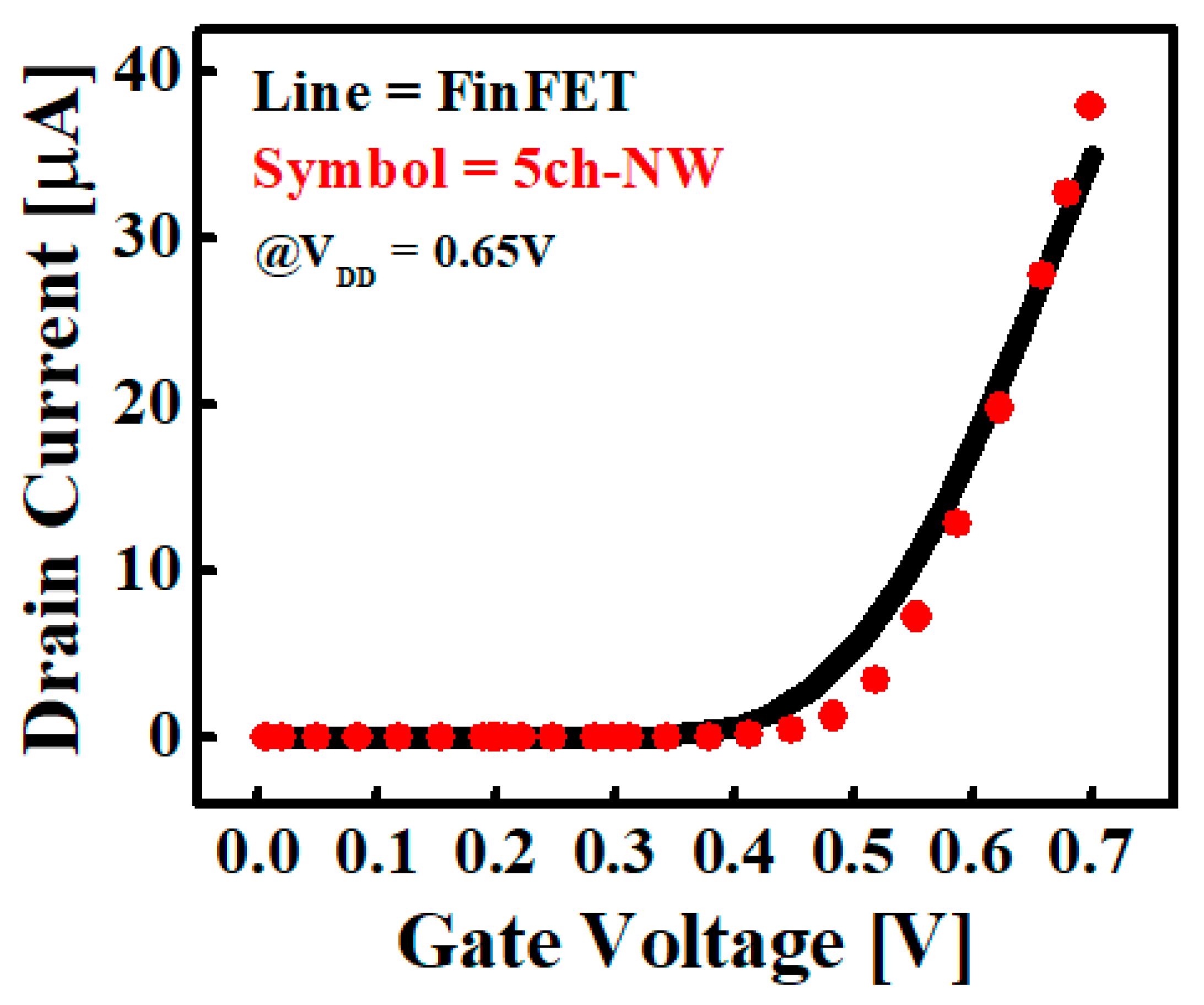
Figure 2.
Black line is the ID-VG curve of the FinFET and the red symbol is the ID-VG curve of the 5ch-NW and shows the calibrated FinFET and 5ch-NW’s ID-VG curve characteristics for similar conditions. Both were extracted by sweeping VG from 0 to 0.7 V when VDD = 0.65 V.
Figure 2.
Black line is the ID-VG curve of the FinFET and the red symbol is the ID-VG curve of the 5ch-NW and shows the calibrated FinFET and 5ch-NW’s ID-VG curve characteristics for similar conditions. Both were extracted by sweeping VG from 0 to 0.7 V when VDD = 0.65 V.

Figure 3.
Structure of each device and the interface hole traps after the total ionizing dose (TID) simulation. (a) The structure of the FinFET; (b) the single-stage structure of 5ch-NW; (c) the interface trap of the FinFET; (d) the interface trap of the 5ch-NW.
Figure 3.
Structure of each device and the interface hole traps after the total ionizing dose (TID) simulation. (a) The structure of the FinFET; (b) the single-stage structure of 5ch-NW; (c) the interface trap of the FinFET; (d) the interface trap of the 5ch-NW.

Figure 4.
TID simulation method of the FinFET. (a) The VG-transient time; (b) the VT shift due to the interface trap.
Figure 4.
TID simulation method of the FinFET. (a) The VG-transient time; (b) the VT shift due to the interface trap.

Figure 5.
ID-VG curve shifts with an increasing radiation dose up to 100 Mrad for (a) FinFET, and (b) 5ch-NW. The ID-VG curves were extracted at 100 krad, 1 Mrad, 10 Mrad, and 100 Mrad. These graphs were obtained by sweeping VDD = 0.65 V and VG from 0 V to 0.7 V when the total dose was reached. (c,d) are the ID-VG curve graph of the log scale of each device according to the TID effect. (c) is the FinFET’s log scale curve, (d) is the 5ch-NW’s log scale curve, (e) is the FinFET’s transconductance graph, and (f) is the 5ch-NW’s transconductance graph.

Figure 6.
FinFET and 5ch-NW extracted the VT shift amount according to the increasing TID.

Figure 7.
Simulation results according to VDD variation (a) FinFET curves, (b) 5ch-NW curves. (c) Comparison of the VT shifts of FinFET and 5ch-NW.
Figure 7.
Simulation results according to VDD variation (a) FinFET curves, (b) 5ch-NW curves. (c) Comparison of the VT shifts of FinFET and 5ch-NW.

Figure 8.
The simulation results according to channel doping. (a) FinFET, (b) 5ch-NW.


Table 1.
Design specifications of the FinFET and 5ch-NW.
| Condition Factor | FinFET | 5ch-NW |
|---|---|---|
| S/D Doping | 1 × 10²¹ (cm−3) | 1 × 10²¹ (cm−3) |
| Channel Doping | 1 × 10¹⁶ (cm−3) | 1 × 10¹⁶ (cm−3) |
| EOT | 0.812 (nm) | 0.812 (nm) |
| Tfin, Dnw/Lg | 6/12 (nm) | 6/12 (nm) |
| Hfin, Hnw | 42 (nm) | 30 (nm) |
| Total area (HfO2 + SiO2 + Silicon) | 489.5 (nm2) | 474.9 (nm2) |
| Oxide area (HfO2 + SiO2) | 237.5 (nm2) | 333.6 (nm2) |
| Parameter explanation | ||
| Tfin: FinFET’s width | Dnw: 5ch-NW’s diameter | |
| Lg: channel length | Hfin: FinFET’s height | |
| Hnw: 5ch-NW’s total height | ||
Table 2.
VT data of each device according to the amount of TID.
| VDD = 0.65 V | FinFET (VT) | 5ch-NW (VT) |
|---|---|---|
| Initial | 329 mV | 402 mV |
| 100 k (rad) | 325 mV | 402 mV |
| 1 M (rad) | 323 mV | 400 mV |
| 10 M (rad) | 312 mV | 388 mV |
| 100 M (rad) | 281 mV | 360 mV |
Table 3.
VT shift according to the VDD variation.
| FinFET (ΔVT) | 5ch-NW (ΔVT) | |||
|---|---|---|---|---|
| VDD = 0.1 V | VDD = 0.65 V | VDD = 0.1 V | VDD = 0.65 V | |
| 100 k (rad) | 1 mV | 4 mV | 0 mV | 0 mV |
| 1 M (rad) | 3 mV | 6 mV | 2 mV | 2 mV |
| 5 M (rad) | 11 mV | 12 mV | 6 mV | 6 mV |
| 10 M (rad) | 17 mV | 17 mV | 14 mV | 14 mV |
Table 4.
VT variation according to the channel doping.
| FinFET (ΔVT) | 5ch-NW (ΔVT) | |||
|---|---|---|---|---|
| Channel doping | 1 × 1016 cm−3 | 1 × 1018 cm−3 | 1 × 1016 cm−3 | 1 × 1018 cm−3 |
| Initial | 329 mV | 345 mV | 402 mV | 411 mV |
| 10 Mrad | 312 mV | 329 mV | 388 mV | 398 mV |
| ΔVT (%) | 5.16% | 4.63% | 3.48% | 3.16% |
© 2019 by the authors. Licensee MDPI, Basel, Switzerland. This article is an open access article distributed under the terms and conditions of the Creative Commons Attribution (CC BY) license (http://creativecommons.org/licenses/by/4.0/).
Share and Cite
MDPI and ACS Style
Won, H.; Ham, I.; Jeong, Y.; Kang, M. Comparison of Various Factors Affected TID Tolerance in FinFET and Nanowire FET. Appl. Sci. 2019, 9, 3163. https://doi.org/10.3390/app9153163
AMA Style
Won H, Ham I, Jeong Y, Kang M. Comparison of Various Factors Affected TID Tolerance in FinFET and Nanowire FET. Applied Sciences. 2019; 9(15):3163. https://doi.org/10.3390/app9153163
Chicago/Turabian StyleWon, Hyeonjae, Ilsik Ham, Youngseok Jeong, and Myounggon Kang. 2019. "Comparison of Various Factors Affected TID Tolerance in FinFET and Nanowire FET" Applied Sciences 9, no. 15: 3163. https://doi.org/10.3390/app9153163
Note that from the first issue of 2016, this journal uses article numbers instead of page numbers. See further details here.