Article

Influence of the Localization of Ge Atoms within the Si(001)(4 × 2) Surface Layer on Semicore One-Electron States

by
Olha I. Tkachuk
1,*,
Maria I. Terebinskaya
1,
Victor V. Lobanov
1 and
Alexei V. Arbuznikov
2
1
O.O. Chuiko Institute of Surface Chemistry, 17 Generala Naumova St., 03164 Kyiv, Ukraine
2
Institut fuer Chemie, Technische Universitaet Berlin, Strasse des 17. Juni 135, D-10623 Berlin, Germany
*
Author to whom correspondence should be addressed.
Computation 2016, 4(1), 14; https://doi.org/10.3390/computation4010014
Submission received: 24 December 2015 / Revised: 18 February 2016 / Accepted: 23 February 2016 / Published: 3 March 2016

Abstract

:
Adsorption complexes of germanium on the reconstructed Si(001)(4 × 2) surface have been simulated by the Si96Ge2Н84 cluster. For Ge atoms located on the surface layer, DFT calculations (B3LYP/6-31G**) of their 3d semicore-level energies have shown a clear-cut correlation between the 3 d 5 / 2 chemical shifts and mutual arrangement of Ge atoms. Such a shift is positive when only one Ge atom penetrates into the crystalline substrate, while being negative for both penetrating Ge atoms. We interpret these results in terms of the charge distribution in clusters under consideration.

1. Introduction

Experimental and theoretical study of Ge on Si quantum dots is one of the exciting modern topics because of their great potentiality in producing thin-film solar cells, high figure-of-merit thermoelectric materials, and other thermo- and optoelectronic devices [1,2,3]. A number of parallel or sequential processes normally occur as soon as a heterojunction between a germanium quantum dot and reconstructed Si(001)(4 × 2) surface is formed [4,5]. The most important of those processes is the formation of =Ge-Ge= surface dimers on the top of a series of asymmetric =Si-Si= species located on the buckled surface. Taking into account a similarity between Si and Ge covalent radii (1.17 and 1.22 Å, respectively [6]), a diffusion penetration of Ge atoms into the crystalline substrate simultaneously with a displacement of an equivalent amount of Si atoms towards the surface may take place. As the result, a formation of mixed =Si-Ge= surface dimers is possible. Together with the thermal motion, those processes reduce the abruptness of the Ge/Si heterojunction [7,8] and hence deteriorate the robustness of corresponding solid state electronic devices. Therefore, a reliable location of the Ge sites on the Ge/Si interface between a germanium quantum dot and Si(001)(4 × 2) crystalline substrate presents an important task.
For such molecular systems as solid-state adsorption complexes, the most precise and exhausting information on the local environment of atoms can be extracted from photoelectron spectra [4]. In particular, the latter can be adequately interpreted in terms of the density of one-electron states over a wide energy range, as soon as corresponding theoretical models are available [9,10]. The interpretation of photoelectron spectra is facilitated by their classification into three regions according to the binding energies of electrons ( E i ) [9]. The first region (0–5 eV) includes a poorly resolvable and rather complicated structure due to the electrons from valence molecular orbitals (MOs) that mainly consist of the atomic orbitals (AOs) belonging to partially occupied electron subshells. The structure of the second region (ca. 15–50 eV) is usually well resolved and can be associated with the linear combinations of semicore AOs originating from closed (sub)shells. The latter, in contrast to valence AOs, in some cases can be combined to so-called internal MOs (IMOs) [11,12]. In the case of adsorption complexes, the formation of those IMOs can be monitored by the exaggerated binding energies of adatoms. Finally, the lines belonging to the third region of photoelectron spectra (>50 eV) are almost solely associated with the core-shell (deep-core) AOs that normally do not contribute to IMOs.
Binding energies of semicore and deep-core electrons are specific for atoms of each element, and analysis of their shifts ( Δ E i ) relative to corresponding reference values is widely employed in determining the composition of an object under study. (Reference binding energies are usually related to either an isolated atom or some reference compound.) Depending on the nature of a molecular system that contains an atom of interest, Δ E i may take values from a few to ten and even more electronvolts (eV). In real solids their translational symmetry breaks at the surface that naturally changes the states of surface atoms vs. bulk ones. As the result, an additional shift occurs depending on whether a given atom located in bulk or in the subsurface region consisting of several monolayers. Such a shift of semicore-level energies typically ranges from ca. 0.01 to 0.5 eV [4].
In this paper we report on the calculated densities of one-electron states for a number of clusters with the same brutto formula Si96Ge2Н84. Thus, so-called cluster A (Figure 1a) simulates a fragment of the Si(001)(4 × 2) relaxed surface with the =Ge-Ge= surface dimer located over the series of =Si-Si= surface dimers. Clusters А1, А2, А3, and А4 (Figure 1b–e, respectively) correspond to different localizations of Ge atoms within the subsurface region of the substrate.

2. Computational Details

Theoretical spectra of one-electron states and, in particular, those of core shells are usually represented as line intensities vs. electron binding energy. Within the linear-combination-of-atomic-orbitals (LCAO) representation, we have calculated the total density of one-electron states, N Ω ( E ) , according to the formula below [13,14,15]:
N Ω ( E ) = m k | c k m | 2 δ ( E ε k )
where c k m is the corresponding LCAO expansion coefficient, k is the summation index over basis-set functions, m—over atoms that constitute a cluster, and ε k is the Kohn-Sham orbital energy. In particular, for a selected atom m, the local density of the states reads as follows:
N Ω ( m ) ( E ) = k | c k m | 2 δ ( E ε k )
For a finite cluster, upon substitution of the delta function by a Gaussian one, we get:
N Ω ( m ) ( E ) = ( 2 π σ ) 1 / 2 k | c k m | 2 exp [ ( E ε k ) 2 / 2 σ 2 ]
For a given line, such an approach yields the intensity which is proportional to the number of one-electron energy levels per unit energy interval and numerically depends on the choice of parameter σ .
To represent the simulated photoelectron spectra, one can employ either an absolute energy scale, or a relative one where the binding energy in the corresponding isolated atom is taken as zero. Moreover, to minimize systematic errors of quantum-chemical calculations, scaling factors are often used when comparing theoretical and experimental data. Thus, experimental binding energy of 1s electron in germanium atom Ge(1s) is 11,104.0 eV [6], while our calculations yield 10,850.5 eV, i.e., their ratio is equal to 1.0234. Such a factor has just been employed in this work to process the results of our calculations. The practice of using scaling factors of such a kind has been justified, e.g., in calculations of the chemical shift for N(1s) line in nitrogen-containing carbon nanoclusters [16,17].
For brevity, chemical shifts are called positive for atoms whose core-level binding energies are higher than those in isolated atoms, and negative otherwise.
Calculations of the equilibrium geometry and electronic structure of the clusters under consideration (Figure 1) have been performed within the framework of Kohn-Sham density functional theory, using hybrid B3LYP exchange-correlation functional [18,19,20,21] and 6-31G** basis set. The choice of such a computational protocol seems to be adequate judging from the success of other theoretical simulations available in literature. One can mention, for instance, Kohn-Sham DFT studies of both the structure of the reconstructed [(1 × 2), (2 × 2), (4 × 2)] pure Si(001) surface [22,23,24] and thermochemical aspects of formation of surface dimers >Ge-Ge<, >Si-Si< and >Si-Ge< on such a surface [25]. Different exchange-correlation functionals (including B3LYP) within different theoretical frameworks (cluster approach, periodic boundary conditions) have been employed in those studies. Corresponding results are in a good agreement with both higher-level theoretical calculations and experimental data.
To take into account the spin-orbit coupling, we have used atomic mean-field (AMFI) approximation [26]. General Atomic and Molecular Electronic Structure System (GAMESS) suite of programs [27] has been employed in our calculations.

3. Results and Discussion

We have shown in our previous study [28] that cluster A characterized by a pure =Ge-Ge= surface dimer is the most stable (the binding energy of the latter with the substrate is ca. 12 eV), while total energies of Clusters A1–A4 with either pure =Si-Si= surface dimer (A2 and A3) or mixed =Si-Ge= one (A1 and A4) are somewhat higher. Therefore, the substitution of germanium atoms in a =Ge-Ge= dimer by one or two substrate silicon atoms is an endothermic process (Table 1).

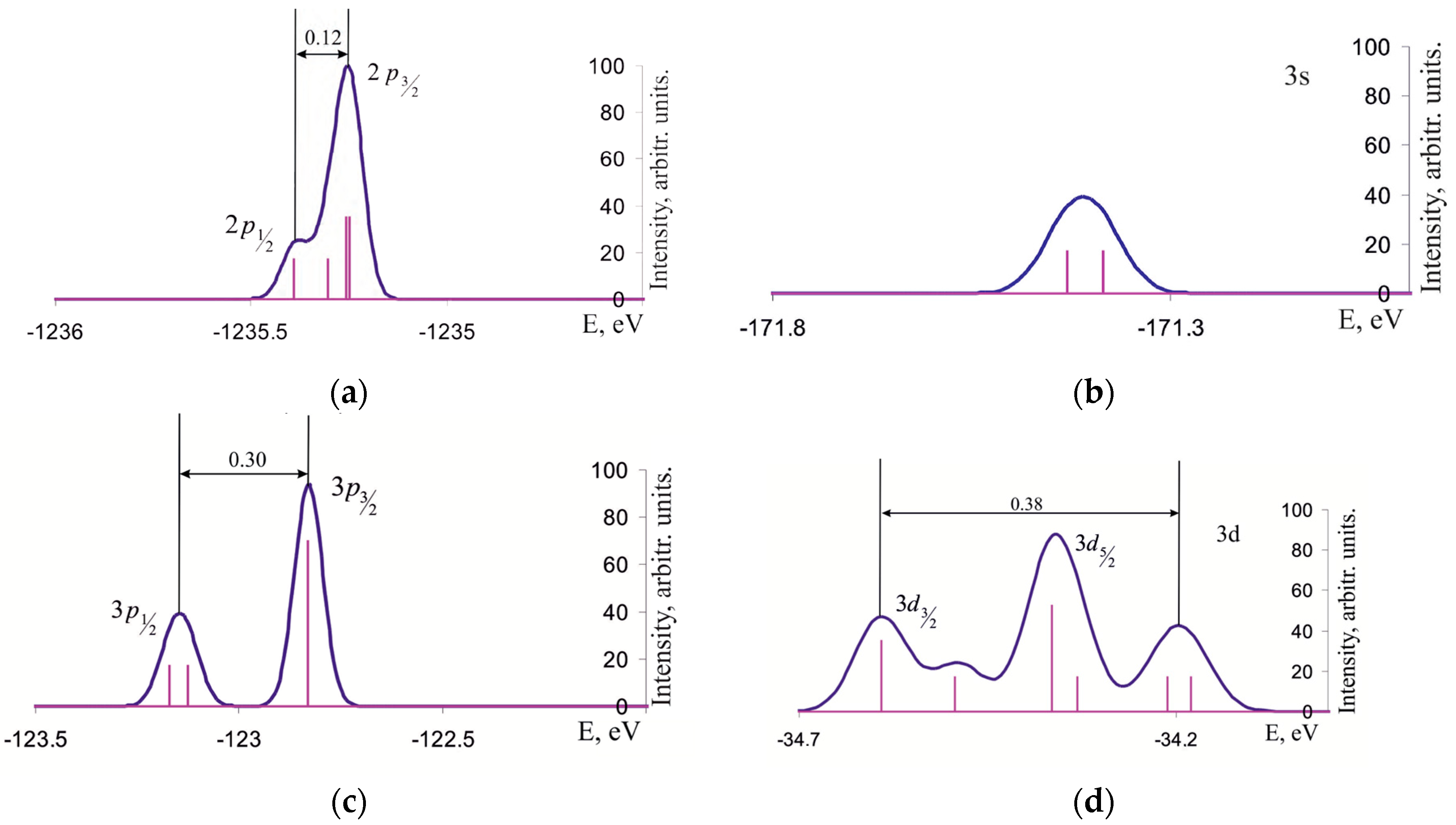
3.1. Density of One-Electron States of Ge2 Molecule

Figure 2 depicts the position of lines corresponding to the binding energies of 2p, 3s, 3p and 3d electrons of isolated Ge2 molecule. Doublet character of 2p and 3p levels is due to the spin-orbit interaction which splits them into 2 p 1 / 2 , 2 p 3 / 2 , and 3 p 1 / 2 , 3 p 3 / 2 components with the splitting values of 0.12 and 0.30 eV, respectively. The spectrum of Ge ( 3 d ) density of states has a more complicated structure. Namely, in addition to the peaks corresponding to 3 d 3 / 2 and 3 d 5 / 2 components, two additional maxima arise due to the formation of IMOs from AOs corresponding to the closed 3d semicore shell which participates in the Ge-Ge binding.

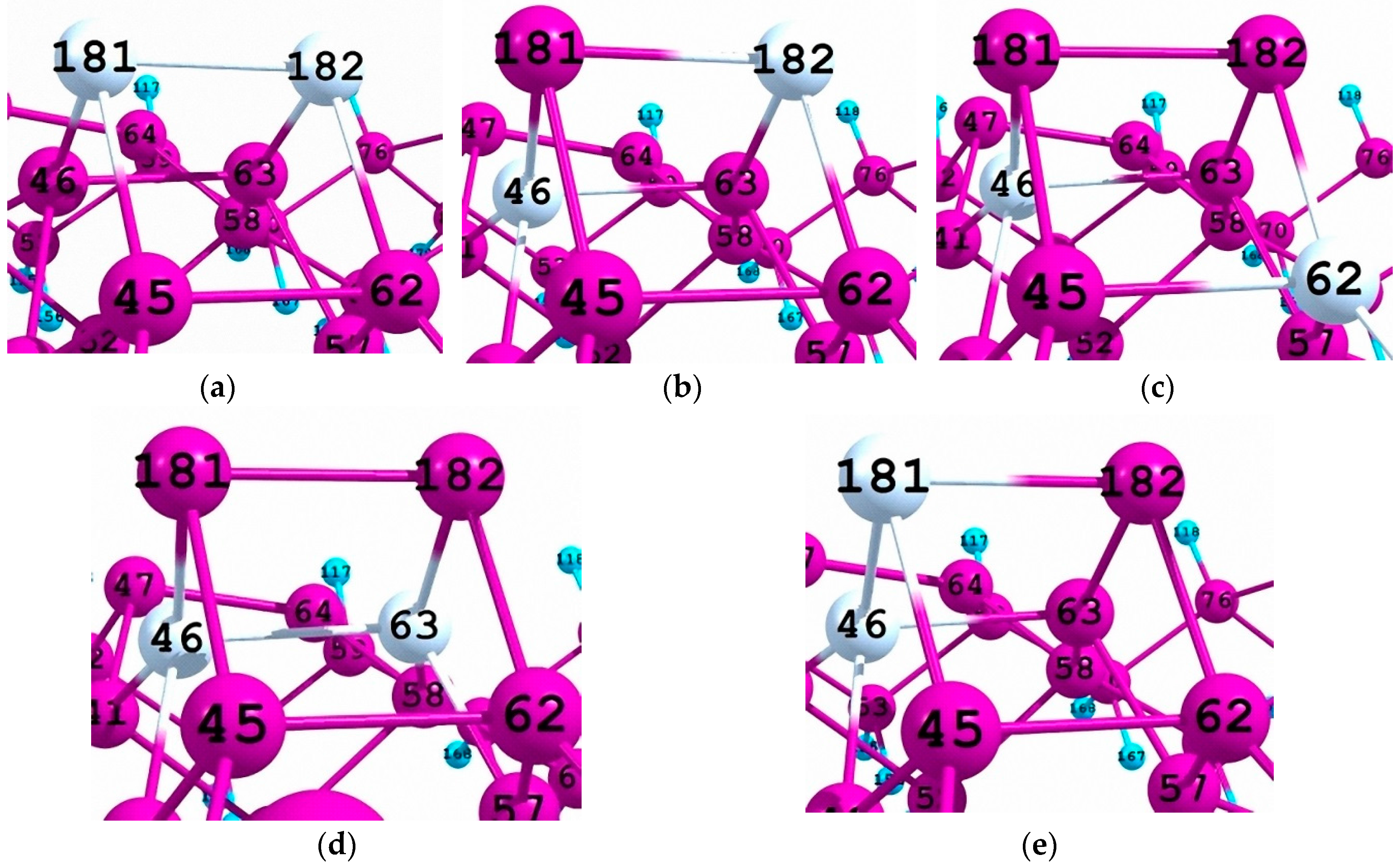
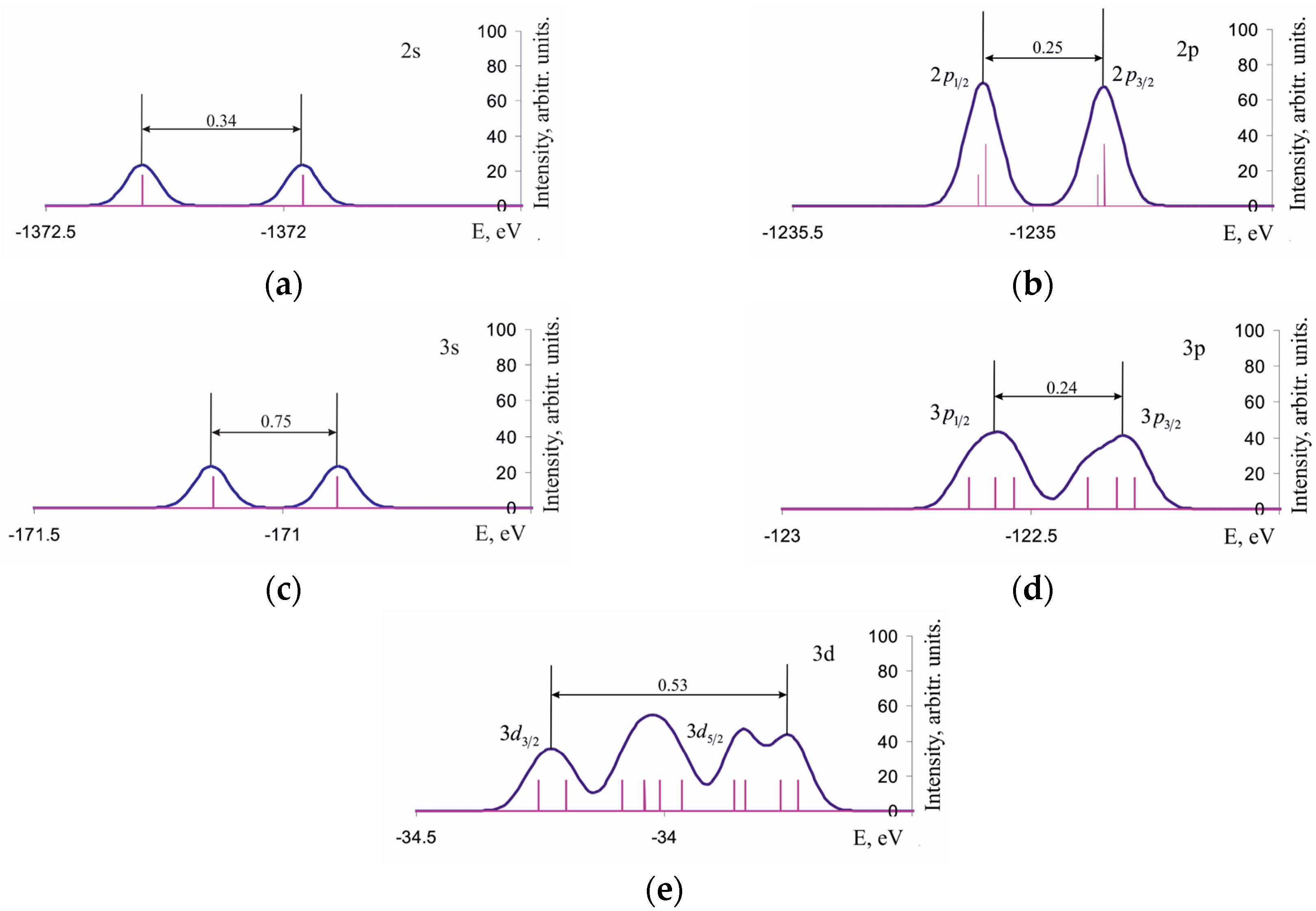
3.2. Density of One-Electron States of Si96H84Ge2 Cluster

The density of one-electron states of the Si96H84Ge2 cluster (Figure 3) shows a bimodal shape for 2s and 3s lines originating from the non-equivalency of Ge atoms within the =Ge-Ge= surface dimer of the reconstructed Si(001)(4 × 2) surface, one of those Ge atoms being in a so-called down-, and another in up-position [28]. Moreover, the intensities of 2 p 3 / 2 and 2 p 1 / 2 components are essentially the same, as well as those of 3 p 3 / 2 and 3 p 1 / 2 , that contradicts theoretical expectations based on the population of the corresponding levels (in contrast to the isolated Ge2 molecule where those expectations are justified). The Ge(3d) line deviates from the bimodal shape and, to a certain extent, keeps the shape motif of the corresponding line of Ge2 molecule. It is important to note that not only the IMO formation but also the abovementioned non-equivalence of Ge atoms within the =Ge-Ge= surface dimer sophisticates the shape of the Ge(3d) line. That might indirectly confirm the presence of Ge2 molecules within the adsorption phase of the Si(001)(4 × 2) surface, despite the calculated Ge-Ge bond lengths are 2.16 Å and 2.21 Å in the =Ge-Ge= surface dimer and in the isolated Ge2 molecule, respectively.
Analysis of the deep-core and semicore electron densities of states within the energy ranges of germanium 1s, 2s, 2p, 3s, 3p, and 3d levels indicates the position of 3d level to be the most sensitive one with respect to the mutual arrangement of Ge and Si atoms within all the clusters under consideration.

3.3. Chemical Shifts of the 3 d 5 / 2 Spin-Orbit Component inClusters A1–A4

Calculated energy shifts of the 3 d 5 / 2 spin-orbit component in Clusters A1–A4 relative its position in Cluster A (Table 1) shows that the migration of germanium atoms from the =Ge-Ge= surface cluster into the bulk substrate increases the absolute values of 3d binding energies for Clusters A1 and A4 (one Ge atom is within the mixed =Si-Ge= surface dimer, and another is in the bulk), but decreases them for Clusters A2 and A3 (pure =Si-Si= surface dimer and both germanium atoms are in the bulk). Such an effect is less pronounced in the latter case.
Rationalization of the calculated data can be carried out in terms of the effective Mulliken charges on atoms and charge transfer between them that are so popular in the world of chemistry. In principle, for both core and valence electrons, their binding energies are determined by the electrostatic potential imposed by electrons and nuclei of the entire molecule or crystal. Thus, the electronic binding energy is a sophisticated function of the spatial structure and electron density distribution of a system under consideration. Analysis of data on the interpretation of chemical shifts in photoelectron spectra shows a very good agreement between calculated and experimental E i values even in the framework of such a rough “electrostatic potential approximation”. According to the latter, a variation of the core-electron binding energy for a given atom is just a function of its effective charge (q) and charges of other atoms (i.e., atomic centers are approximated by Coulomb-interacting point charges). Therefore, one can formulate the basic dominant trend for the behavior of a semicore-electron binding energy as follows: E i for a given atom increases as its electron density is depleted (displaced towards neighboring atoms) and decreases otherwise.
According to the scheme accepted, a binding energy of a semicore electron is determined by two factors: (i) formal oxidation state of an atom which can be roughly identified with its formal charge; and (ii) relative donor-acceptor properties of this atom as well as those of its neighbors (as the “neighboring atoms”, we hereafter mean those directly bonded to a given atom).
As follows from Table 2, two germanium atoms (Nos. 181 and 182) entering the =Ge-Ge= dimer in Cluster A are charged negatively, while the sum of charges on their neighbors is positive. In Cluster A1, Ge(46) atom is embedded into the substrate, and its negative charge increases to −0.081 atomic units (a.u.) (while that of Ge(182)) amounts to −0.065 a.u.), and the positive sum of charges on the neighboring atoms (0.074 and 0.118 a.u. for Ge(46) and Ge(182), respectively) increases comparing to Cluster A as well. As the result, a positive chemical shift of the semicore-electron binding energy relative Cluster A is observed.
Cluster А2 contains Ge(46) and Ge(62) atoms within the crystalline substrate, whose charges are −0.023 and −0.010 a.u., respectively, while the sum of charges on neighboring atoms is also positive, but significantly smaller than that for Cluster A. According to the electrostatic potential approximation, that leads to a negative chemical shift, as one could expect.
The situation seems to be more complicated for Cluster А3 because of an invariance of the charge on Ge(46) comparing to Cluster A, and a decrease of the negative charge on Ge(63) to −0.006 a.u. Together with a negative sum of charges on neighboring atoms, these circumstances enhance the role of the second factor, i.e., donor-acceptor properties of surrounding silicon atoms and thus explain the negative chemical shift.
In Cluster A4, Ge atoms are directly bonded to each other, while one of them Ge(181) enters =Si-Ge= mixed dimer and another Ge(46) is located within the crystalline substrate. The charge of the latter atom amounts to −0.118 a.u., and the sum of charges on its neighbors is +0.116 a.u. Such a charge distribution (similar to that of Cluster A1) results in a positive 3 d 5 / 2 chemical shift of the Ge(3d) line.

4. Conclusions

We have calculated semicore-level energy shifts for adsorption complexes simulated by a series of clusters with the same brutto formula Si96Ge2Н84 but different arrangements of germanium atoms within the surface layer and bulk. Their comparison with a similar spectrum of the isolated Ge2 molecule has led us to the following conclusions:
(i)
Atomic orbitals from the closed d shell of germanium atom contribute to internal molecular orbitals that are responsible for a high binding energy of the =Ge-Ge= surface dimer.
(ii)
For Si96Ge2Н84 clusters containing only one germanium atom embedded in a crystalline silicon substrate, a 3 d 5 / 2 chemical shift of the Ge(3d) line is positive (i.e., the binding energy of the corresponding electrons is higher comparing to that in the cluster containing =Ge-Ge= surface dimer). For clusters with both germanium atoms embedded in a substrate, such a chemical shift is negative.

Author Contributions

Olha I. Tkachuk and Maria I. Terebinskaya have performed all the calculations and actively participated in analyzing the results and writing the paper. Olha I. Tkachuk has also personally presented the results at the DFT-2015 Conference in Debrecen (Hungary). The problem has been formulated by Victor V. Lobanov who actually supervised this study, including writing the paper. Extensive discussions of the results and assistance in formulating the content of this work in English were due to Alexei V. Arbuznikov.

Conflicts of Interest

The authors declare no conflict of interest.

References

  1. Lozovoy, K.A.; Voytsekhovskiy, A.V.; Kokhanenko, A.P.; Satdarov, V.G.; Pchelyakov, O.P.; Nikiforov, A.I. Heterostructures with self-organized quantum dots of Ge on Si for optoelectronic devices. Opto-Electron. Rev. 2014, 22, 171–177. [Google Scholar] [CrossRef]
  2. Liu, Z.; Zhou, T.; Li, L.; Zuo, Y.; He, C.; Li, C.; Xue, C.; Cheng, B.; Wang, Q. Ge/Si quantum dots thin film solar cells. Appl. Phys. Lett. 2013, 103, 082101. [Google Scholar] [CrossRef]
  3. Chang, H.-T.; Wang, S.-Y.; Lee, S.-W. Designer Ge/Si composite quantum dots with enhanced thermoelectric properties. Nanoscale 2014, 6, 3593–3598. [Google Scholar] [CrossRef] [PubMed]
  4. Gomoyunova, M.G.; Pronin, I.I. Photoelectron spectroscopy of atomic core-shell levels at silicon surface. Zhurnal Tekhnicheskoi Fiziki 2004, 74, 1–34. (In Russian) [Google Scholar]
  5. Shklyaev, A.A.; Ichikawa, M. Creation of germanium and silicon nanostructures using scanning tunneling microscope. Uspekhi Fizicheskikh Nauk 2006, 176, 913–930. (In Russian) [Google Scholar] [CrossRef]
  6. Cotton, F.A.; Wilkinson, G. Advanced Inorganic Chemistry, 3rd ed.; Wiley: New York, NY, USA, 1972. [Google Scholar]
  7. Ratto, F.; Locatelli, A.; Fontana, S.; Kharrazi, S.; Ashtaputre, S.; Kulkarni, S.K.; Heun, S.; Rosei, F. Diffusion Dynamics during the Nucleation and Grown Ge/Si Nanoctructures on Si(111). Phys. Rev. Lett. 2006, 96, 096103. [Google Scholar] [CrossRef] [PubMed]
  8. Simonsen, A.C.; Schleberger, M.; Tougaard, S.; Hansen, J.L.; Larsen, A.N. Nanoctructure of Ge deposited on Si(111): A study by XPS peak shape analysis and AFM. Thin Solid Films 1999, 338, 165–171. [Google Scholar] [CrossRef]
  9. Siegbahn, K.; Nordling, C.; Fahlman, A.; Nerdberg, R.; Hamrin, K.; Hedman, J.; Johansson, G.; Bergmark, T.; Karlsson, S.-E.; Lindgrem, I.; et al. ESCA Atomic, Molecular and Solid State Structure Studied by Means of Electron Spectroscopy; Almqvist & Wiksells Boktryckeri AB: Uppsala, Sweden, 1967. [Google Scholar]
  10. Briggs, D.; Seah, M.P. Practical Surface Analysis. Auger and X-ray Photoelectron Spectroscopy, 2nd ed.; Wiley: New York, NY, USA, 1990. [Google Scholar]
  11. Teterin, Y.A.; Gagarin, S.G. Internal valence molecular orbitals of compounds and structure of photoelectron spectra. Uspekhi Khimii 1996, 65, 895–919. (In Russian) [Google Scholar]
  12. Ku, W.; Eguiluz, A.G. Band-gap problem in semiconductors revisited: Effects of core states and many-body self-consistency. Phys. Rev. Lett. 2002, 89, 126401. [Google Scholar] [CrossRef] [PubMed]
  13. Messmer, R.P.; Watkins, G.D. Molecular-orbital treatment for deep levels in semiconductors: Substitutional nitrogen and the lattice vacancy in diamond. Phys. Rev. B 1973, 7, 2568–2590. [Google Scholar] [CrossRef]
  14. Posternac, M.; Krakauer, H.; Freeman, A.J.; Koelling, D.D. Self-consistent electronic structure of surface: Surface states and surface resonance on W(001). Phys. Rev. B 1980, 21, 5601–5312. [Google Scholar] [CrossRef]
  15. Salahub, D.R.; Messmer, R.P. Molecular-orbital study of aluminum clusters containing up to 43 atoms. Phys. Rev. B 1977, 16, 2526–2536. [Google Scholar] [CrossRef]
  16. Abergel, D.S.L.; Apalkov, V.; Berashevich, J.; Zielger, K.; Chakraborty, T. Properties of graphene: A theoretical perspective. Adv. Phys. 2010, 59, 261–482. [Google Scholar] [CrossRef]
  17. Barnarda, A.S.; Snook, I.K. Size- and shape-dependence of the graphene transformation in the absence of hydrogen. J. Mater. Chem. 2010, 20, 10459–10464. [Google Scholar] [CrossRef]
  18. Becke, A.D. Density-functional thermochemistry. III. The role of exact exchange. J. Chem. Phys. 1993, 98, 5648–5652. [Google Scholar] [CrossRef]
  19. Stephens, P.J.; Devlin, F.J.; Chabalowski, C.F.; Frisch, M.J. Ab initio calculation of vibrational absorption and circular dichroism spectra using density functional force fields. J. Phys. Chem. 1994, 98, 11623–11627. [Google Scholar] [CrossRef]
  20. Lee, C.; Yang, W.; Parr, R.G. Development of the Colle-Salvetti correlation-energy formula into a functional of the electron density. Phys. Rev. B 1988, 37, 785–789. [Google Scholar] [CrossRef]
  21. Miehlich, B.; Savin, A.; Stoll, H.; Preuss, H. Results obtained with the correlation energy density functionals of Becke and Lee, Yang and Parr. Chem. Phys. Lett. 1989, 157, 200–206. [Google Scholar] [CrossRef]
  22. Konecny, R.; Doren, D.J. Adsorption of water on Si(100)-(2 × 1): A study with density functional theory. J. Chem. Phys. 1997, 106, 2426–2435. [Google Scholar] [CrossRef]
  23. Yang, C.; Kang, H.C. Geometry of dimer reconstruction on the C(100), Si(100), and Ge(100) surfaces. J. Chem. Phys. 1999, 110, 11029–11037. [Google Scholar] [CrossRef]
  24. Penev, E.; Kratzer, P.; Scheffler, M. Effect of the cluster size in modeling the H2 desorption and dissociative adsorption on Si(001). J. Chem. Phys. 1999, 110, 3986–3994. [Google Scholar] [CrossRef]
  25. Gay, S.C.A.; Srivastava, G.P. Dimer length variation for different reconstructions of Si, Ge, and mixed Si-Ge dimers on Si(001) and Ge(001) substrates. Phys. Rev. B 1999, 60, 1488–1492. [Google Scholar] [CrossRef]
  26. Hess, B.A.; Marian, C.M.; Wahlgren, U.; Gropen, O. A mean-field spin-orbit method applicable to correlated wavefunctions. Chem. Phys. Lett. 1996, 251, 365–371. [Google Scholar] [CrossRef]
  27. Schmidt, M.W.; Baldridge, K.K.; Boatz, J.A.; Elbert, S.T.; Gordon, M.S.; Jensen, J.H.; Koseki, S.; Matsunaga, N.; Nguyen, K.A.; Su, S.; et al. General atomic and molecular electronic-structure system. Review. J. Comput. Chem. 1993, 14, 1347–1363. [Google Scholar] [CrossRef]
  28. Tkachuk, O.I.; Terebinska, M.I.; Lobanov, V.V. Structure of the dimeric adsorption complex Ge on the face of Si(001). Surface 2013, 5, 26–33. (In Ukrainian) [Google Scholar]
Figure 1. (a) Configuration of the adsorption complex А (Si96H84·Ge2) with a pure =Ge-Ge= dimer on the top of a series of surface =Si-Si= dimers; (b) Cluster A1; (c) Cluster A2; (d) Cluster A3; (e) Cluster A4. Clusters A1–A4 are formed from Cluster A as the result of a substitution of one or two surface Ge atoms by Si atoms of the substrate.
Computation 04 00014 g001
Figure 2. Density of the semicore one-electron states for the isolated Ge2 molecule within the binding-energy ranges of (a) 2p; (b) 3s; (c) 3p; and (d) 3d electrons of the Ge atom.
Computation 04 00014 g002
Figure 3. Density of the core one-electron states for Cluster A within the binding-energy ranges of (a) 2s; (b) 2p; (c) 3s; (d) 3p; and (e) 3d electrons of the Ge atom.
Computation 04 00014 g003
Table 1. Calculated relative energies of Clusters A1–A4 and chemical shifts for the 3 d 5 / 2 component of the Ge(3d) line. Cluster A is taken as the reference (see Figure 1).
ClusterA1A2A3A4
Relative energy, kcal/mol1.835.152.725.11
Chemical shift, eV+0.12−0.08−0.07+0.10
Table 2. Mulliken charges (a.u.) on Ge atoms and sums of charges on neighboring Si atoms.
Number of an Atom in the ClusterChemical Symbol of an AtomAtomic ChargeSum of Charges on Neighboring Atoms
Cluster А
181Ge−0.0680.042
182Ge−0.0700.040
45Si0.068−0.179
62Si0.039−0.103
63Si0.071−0.098
46Si0.044−0.112
Cluster А1
181Si0.018−0.095
182Ge−0.0650.118
45Si0.051−0.108
62Si0.008−0.094
63Si0.092−0.216
46Ge−0.0810.074
Cluster А2
181Si0.014−0.021
182Si0.027−0.050
45Si0.075−0.224
62Ge−0.0100.095
63Si0.081−0.165
46Ge−0.0230.029
Cluster А3
181Si0.020−0.037
182Si0.032−0.001
45Si−0.004−0.107
62Si−0.015−0.043
63Ge−0.006−0.030
46Ge−0.065−0.023
Cluster А4
181Ge−0.1180.096
182Si−0.0140.125
45Si0.014−0.055
62Si0.032−0.151
63Si0.111−0.250
46Ge−0.0960.116

