Artificial 2D van der Waals Synapse Devices via Interfacial Engineering for Neuromorphic Systems
by
 and
and
Woojin Park
1, 
Hye Yeon Jang
1,
Jae Hyeon Nam
1,
Jung-Dae Kwon
2,
Byungjin Cho
1,* and
Yonghun Kim
2,* 
1
Department of Advanced Material Engineering, Chungbuk National University, Chungdae-ro 1, Seowon-Gu, Cheongju, Chungbuk 28644, Korea
2
Materials Center for Energy Convergence, Surface Technology Division, Korea Institute of Materials Science (KIMS), 797 Changwondaero, Sungsan-gu, Changwon, Gyeongnam 51508, Korea
*
Authors to whom correspondence should be addressed.
Nanomaterials 2020, 10(1), 88; https://doi.org/10.3390/nano10010088
Submission received: 22 November 2019
/
Revised: 28 December 2019
/
Accepted: 31 December 2019
/
Published: 2 January 2020
(This article belongs to the Special Issue Preparation and Properties of 2D Materials)
Abstract
:Despite extensive investigations of a wide variety of artificial synapse devices aimed at realizing a neuromorphic hardware system, the identification of a physical parameter that modulates synaptic plasticity is still required. In this context, a novel two-dimensional architecture consisting of a NbSe2/WSe2/Nb2O5 heterostructure placed on an SiO2/p+ Si substrate was designed to overcome the limitations of the conventional silicon-based complementary metal-oxide semiconductor technology. NbSe2, WSe2, and Nb2O5 were used as the metal electrode, active channel, and conductance-modulating layer, respectively. Interestingly, it was found that the post-synaptic current was successfully modulated by the thickness of the interlayer Nb2O5, with a thicker interlayer inducing a higher synapse spike current and a stronger interaction in the sequential pulse mode. Introduction of the Nb2O5 interlayer can facilitate the realization of reliable and controllable synaptic devices for brain-inspired integrated neuromorphic systems.
1. Introduction
Continuous downscaling has stimulated the development of semiconductor technology for the last several decades, offering advantages, such as lower power consumption, higher integration, faster circuit operation, and reduced device cost per function. However, the side effects from continuous downscaling, to a size of less than 10 nm, limit the further development of the silicon semiconductor technology. This has motivated the exploration of novel computation systems beyond the conventional Von Neumann architecture that can overcome the downscaling limitations. Recently, due to the increasing need to implement sophisticated information processing system mimicking the human brain, the neuromorphic computing system has attracted a great deal of attention [1,2,3,4,5]. For the integrated neuromorphic systems, it is important to realize operations of complex and diverse functions implemented using a parallel architecture consisting of ~1011 neurons and ~1015 synapses. Additionally, the unit event should be simultaneously conducted using an extremely small amount of energy [6].
The artificial synapse device is considered to be an essential fundamental element for the emulation of biological neural networks [7]. The mechanism of operation for transmitting a spike input stimulus through the synapse can strengthen or weaken the synaptic weight, which is known as synaptic plasticity [8]. The synapse provides the functions of information processing and storage based on the spiking neural network. For this system, conventional solid-state electronics technology has been adopted for emulating the biological synapse function, in order to demonstrate a neuromorphic computing system [9]. In previous studies, conventional silicon-based complementary metal-oxide semiconductor (CMOS) technology was employed for demonstrating solid-state synapse devices, and a network consisting of 256 million configurable synapses and 1 million programmable spiking neurons was demonstrated [10]. The use of the 28-nm fully depleted silicon-on-insulator CMOS technology for 64k-synapse and 256-neuron architecture was also reported [11]. However, these CMOS-based devices are still unsuitable for realizing an artificial intelligence chip, because they cannot meet the requirements of higher integration density and lower power consumption. Si CMOS-based synapse device is based on the operation of complex logic circuits. This means that its power dissipation is essentially higher than that of other types, which is not satisfactory for emulating the biological synapse with an ultralow femtojoule energy consumption.
To eliminate the bottlenecks hindering the further development of neuromorphic computing systems, three-terminal artificial synaptic transistors, based on novel semiconductors have been studied to demonstrate synaptic functions. For instance, diverse semiconducting materials including carbon nanotubes, [12] nickelate, [13], and indium gallium zinc oxide (IGZO) [14,15] have been selected for the realization of synapse platforms. Meanwhile, two-dimensional (2D) transition dichalcogenides (TMDCs) are an intriguing nanomaterial layer for key elements of synaptic transistors due to their advantages of excellent intrinsic scalability, transparency, chemical robustness, and low power consumption [16,17,18,19]. In fact, several research groups have demonstrated the corresponding synaptic devices [20,21]. Meanwhile, a variety of oxide layers have been used as the conductance-tuning layers for synapse device applications. For example, phase change memory emulating synaptic behavior was demonstrated using a thin HfO2 interface layer [22]. Additionally, Deswal et al. reported an NbOx-based memristor, showing a gradual and continuous conductance change that is a prerequisite of a biological synapse device [23]. Nevertheless, it is still unclear what physical parameters can be used to precisely manipulate the synaptic functions. Thus, the use of a 2D heterostructure, combined with insulating oxide, can be an alternative approach for the development of energy-efficient artificial synapse devices.
In this work, we designed a vertically-stacked 2D metallic electrode NbSe2/semiconductor WSe2/interlayer Nb2O5 heterostructure placed on an Si/SiO2 substrate with the back-gate configuration. Here, WSe2 and Nb2O5 served as the active channel, and the conductance-tuning layer, respectively. Additionally, the NbSe2 electrode can provide excellent transistor switching characteristics due to a sharp 2D interface and the absence of the metal-induced gap states [24,25]. The post-synaptic current behavior can be modulated precisely by adjusting the thickness of the Nb2O5 layer, with a thicker Nb2O5 interlayer providing higher synapse spike current and strong interaction in paired pulse facilitation testing modes. The charge trapping/detrapping mechanism at the Nb2O5 defect states based on an energy band model was proposed. The novel 2D architecture will pave the way toward extreme integration for the development of the massively parallel neuromorphic circuitry system.
2. Materials and Methods
2.1. CVD Synthesis of WSe2 and NbSe2
A selenium (Se)-based semiconducting channel based on WSe2 and a metallic electrode based on NbSe2 were synthesized using a simple two-step process. First, WO3 and Nb2O5 thin films were individually deposited on an SiO2/Si wafer. The thicknesses of the WO3 and Nb2O5 thin films were ~3, and ~5 nm, respectively. This pre-deposited oxide layer on the wafer was directly loaded into the center of thermal furnace and vacuumed with a rotary pump system. Then, the thermal furnace was heated to the desired temperature (~1000 °C) under the flow of 5% hydrogen-balanced Ar gas (Ar/H2), while a selenium powder source was sublimated by heating to 500 °C. After a 1-h selenization process, the furnace was naturally cooled down to room temperature.
2.2. Fabrication of 3-Terminal Synapse Device
A heavily doped p-type Si substrate with SiO2 was cleaned by sonication in acetone, methanol, and iso-propyl alcohol (IPA) solution. To precisely tune the synaptic weight corresponding to the drain current, the charge trapping layer of the Nb2O5 thin film was deposited with different thicknesses using thermal evaporation. The thickness of Nb2O5 varied from 2.6 to 3.9 nm, as validated by the cross-sectional transmission electron microscopy (TEM) analysis. Then, the synthesized WSe2 semiconducting channel was transferred onto an SiO2/Si wafer using a poly(methyl methacrylate)-assisted transfer method and patterned using conventional photolithography. Finally, the NbSe2 metallic electrode was transferred for the formation of the NbSe2/WSe2 van der Waals heterojunction, in order to minimize the contact resistance [24,25].
2.3. Electrical Characterization
Basic electrical characterizations were carried out using a Keithley 2636B source meter (Keithley Instruments, Solon, OH, USA). The amplitude of the applied synaptic pulse, used to generate an excitatory post-synaptic current (EPSC), was 20 V and its duration was varied from 2 to 10 s.
3. Results and Discussion
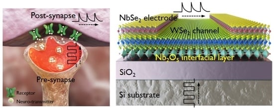
Figure 1a shows a schematic of a biological neural network consisting of synapses and neurons. The most important trait of brain-inspired devices is their capability for efficient data processing using an extremely small amount of power in the networks with an astronomical number of synapses and neurons. The parallel network means that processing and storage of information occur simultaneously and do not follow the von Neumann computing paradigm. Therefore, a high device integration density and low energy consumption are crucial for a neuromorphic system. The operation of transmitting a spike input stimulus is illustrated in Figure 1b. The interaction of the pre- and post-synaptic activities affects the long-lasting connection strength, and long-lasting plasticity is considered to be the key mechanism of basic neuromorphic computation. Figure 1c shows the back-gate configuration of the WSe2 synapse transistor. The heavily-doped Si layer was used as the back-gate and NbSe2 was used as the source/drain. The Nb2O5 interfacial layer allows the fine-tuning of the conductance of the WSe2 transistor.
Figure 2a shows a schematic of the electrical measurements of the synapse device in the back-gate pulse system. Figure 2b shows the obtained cross-sectional high-resolution transmission electron microscopy images and the results of the energy-dispersive X-ray spectroscopy (EDS) analysis, thereby, clearly demonstrating the distinct film layers and sharp junction interfaces. The different stacking structures of WSe2-NbSe2, 2.6 nm Nb2O5-WSe2-NbSe2, and 3.9 nm Nb2O5-WSe2-NbSe2 were clearly observed and compared. The boundaries of each layer appeared to be atomically sharp and smooth without a significant interfacial gap. Five layers of NbSe2 and three layers of WSe2 were consistently observed for all of the samples, and the additional interfacial Nb2O5 layer was also clearly observed. The distributions of the W, Se, Nb, and O elements were obtained from the EDS elemental mapping images. The left panel of Figure 2b shows the WSe2-NbSe2 stack architecture without the Nb2O5 deposition. Since, both the NbSe2 and Nb2O5 films contain Nb atoms, the two separate Nb layers were observed only in the samples with the Nb2O5 interfacial layer, verifying the existence of Nb2O5. The middle panel of Figure 2b shows the results for the sample with a 2.6 nm Nb2O5 layer. The right panel of Figure 2b shows the sample with a 3.6 nm Nb2O5 layer. Figure 2c shows that the Raman spectra obtained for the as-synthesized 2D films support the presence of 2D materials, such as WSe2 and NbSe2, demonstrating the successful synthesis of the 2D nanomaterials via the chemical vapor deposition (CVD) technique. The Raman spectra of WSe2 and NbSe2 clearly display the in-plane vibrational modes of W-Se and Nb-Se (E12g: 250.3 and 243.2 cm−1) and the out-of-plane vibrational modes that arise from the motion the Se atoms (A1g: 258.5 and 230.6 cm−1 for WSe2 and NbSe2). Furthermore, two distinct Raman peaks of WSe2 and NbSe2 with stacked device structure were also observed even after transfer process in Figure S1 in the Supplementary information.
To compare the transfer characteristics of the WSe2-NbSe2 van der Waals hetero-junction devices with different Nb2O5 thickness, DC-mode-based double sweep measurements were performed, as shown in Figure 3a. The double sweep curves of the 2D heterojunction devices were obtained under varying values of able VBG in the range from 10 to −20 V at a fixed drain voltage of −5 V. The WSe2-based transistor showed typical p-type unipolar behavior, with a counterclockwise hysteresis loop, that may be ascribed to the confinement of the hole charges in the trap states induced by the Nb2O5 interlayer [26]. Additionally, the repeatability test of DC transfer double sweep curves, with different Nb2O5 thicknesses, were also shown in Figure S2 in Supplementary information. We also investigated the statistical distribution of the hysteresis window voltages, in order to validate the reliability of the data corresponding to the hysteresis behavior (Figure 3b). The average values of the hysteresis voltage for each device were measured to be ~5, 7, and 11 V, respectively. The value of the error bar was almost same for all of the devices. Thus, it is clear that a thicker Nb2O5 interlayer gives rise to a larger hysteresis window. The dependence of DC sweep speed on transfer curves was also depicted in Figure S3 in Supplementary information.
To elucidate the origin of the hysteresis of the 2D heterostructure transistors, the corresponding energy band model was proposed (Figure 4). We previously reported the positive effect of the combination of WSe2-NbSe2 with reduced contact barrier [24,25]. The conventional Richardson-Schottky equation was employed to calculate Schottky barrier,
where A is the contact area, A* is the effective Richardson constant, T is the temperature, ΦB is the Schottky barrier height, q is the electron charge, V is the applied forward bias, ε0 and εr are the permittivity of the vacuum and the oxide layer, respectively, d is the width of the interface barrier, and Kb is the Boltzmann constant. It was mentioned in the references that Schottky barrier at WSe2-NbSe2 contact is significantly lower than that at WSe2-metal(Pd) contact due to Fermi-level de-pinning. Therefore, the 2D WSe2-NbSe2 combination can be an excellent candidate for the fabrication of an energy-efficient low-power synaptic transistor, due to its low contact resistance. Recently, the new methodology for universal 2D material was reported to obtain Schottky barrier, suggesting more accurate calculation [27]. Holes are known to be the major carriers in both the semiconductor channel WSe2 and the metallic source/drain electrode NbSe2. Thus, only the hole charge transport was considered in our proposed switching model. As shown in Figure 4a, the negative voltage applied to the back gate electrode (p +Si) shifts the corresponding Fermi level upward, accumulating hole charge near the Nb2O5-corresponding defect states. Under a negative gate bias, holes can be easily trapped in the defect states within the Nb2O5 interlayer, depleting the carriers in the WSe2 and leading to a decrease in the drain current. Meanwhile, when a positive voltage is applied to the gate, the Fermi level shifts downward, depleting the trapped holes in the Nb2O5 defects (Figure 4b). Simply put, the trapped holes will be released across the Nb2O5-WSe2 interface, leading to an increase in the drain current. Indeed, we experimentally proved that the amount of the trapped hole carriers is controlled by the Nb2O5 thickness.
To characterize the pulse response of the 2D heterostructure devices, we monitored the spike current response to the gate voltage pulses with the amplitude and duration time of 20 V, and 2 s, respectively (Figure 5a). In neuroscience, it is important to transfer electrical or chemical signal from pre-synapse to post-synapse. This is usually caused by the flow of positively charged ions. EPSC can be generated by the action of ions or electron flow in the neuromorphic system. The gate voltage for the EPSC was fixed at −20 V to give a fair comparison for each case. EPSC reaches the maximum value and then decays back to the initial current state. Interestingly, the spike was generated, even in the reference device without Nb2O5 layer. This might be because of the unintentional charge trap sites, which exist at the diverse interfaces (WSe2-NbSe2 and SiO2-WSe2). Our result showed that the peak values increase with the increasing thickness of the inserted Nb2O5 interlayer. Higher voltage pulses required long decay time to restore the synapse device to the initial current state, leading to stronger nonvolatile properties. The duration time of the pulse voltage, that is applied to the devices also affected the peak EPSC (Figure 5b). A longer pulse duration resulted in a higher peak EPSC. In a biological neural network, paired pulse facilitation is an important synapse parameter for determining synaptic plasticity, that is responsible for learning and memory processes [28]. As shown in Figure 5c, paired pulse facilitation is the phenomenon where the EPSC stimulated by the second spike is enhanced when the first spike is closely followed by the second spike [29,30]. Such essential synapse behavior can be emulated using our 2D heterostructure transistor. Figure 5d shows the interaction of two sequential spikes for all of the devices. The interval time between the applied pulses was 2 s. The interaction between the output spike current of the control device without Nb2O5 was not observed, indicating the negligible synaptic weight modulation property. Meanwhile, the introduction of the Nb2O5 layer strengthened the interaction of the two spikes; more specifically, a thicker Nb2O5 interlayer induced a much greater current change at the second pulse mode. Such a strong tuning ability of the synaptic weight enhances the electrical plasticity of the artificial synapse device, and may improve the intelligence of the integrated neuromorphic system [12].
4. Conclusions
We demonstrated controllable synaptic plasticity with the WSe2/Nb2O5 heterostructure in the WSe2 back-gate device. The Nb2O5 layer served as the conductance-modifying layer and enabled precise modulation of the conductive states and their dynamic change. Essential synaptic functions (EPSC and paired pulse facilitation) were investigated in the WSe2/Nb2O5 heterostructure devices. In particular, the optimized thickness of the Nb2O5 layer strengthened the interaction in the synaptic weight, showing the largest post-synapse current. Thus, the facile one-step Nb2O5 layer deposition process, demonstrated in this work, is an effective approach for the realization of controllable synaptic devices.
Supplementary Materials
The following are available online at https://www.mdpi.com/2079-4991/10/1/88/s1, Figure S1: Raman spectrum of WSe2 and NbSe2 after transfer process, Figure S2: Repeatability test of DC transfer double sweep curves with different Nb2O5 thickness, Figure S3: The dependence of DC sweep speed on transfer curves.
Author Contributions
B.C. and Y.K. designed and conducted the experiments. H.Y.J. and J.H.N. and J.-D.K. supported the execution of the experiments and the data analysis. W.P., B.C., and Y.K. wrote the paper. B.C., and Y.K. supported and guided the experiments and analysis of results. Y.K. conceived the project and supervised the writing of the paper. All authors have read and agreed to the published version of the manuscript.
Funding
This work was supported by the National Research Foundation of Korea (NRF) grant funded by the Korean government (MSIT; Ministry of Science and ICT) (No. 2017R1C1B1005076) and Fundamental Research Program (No. PNK6990) of the Korea Institute of Materials Science (KIMS). This research was also financially supported by the Ministry of Trade, Industry and Energy (MOTIE) and Korea Institute for Advancement of Technology (KIAT) through the National Innovation Cluster R & D program (P0006704_Development of energy saving advanced parts).
Conflicts of Interest
The authors declare no conflict of interest.
References
- Kim, S.; Yoon, J.; Kim, H.D.; Choi, S.J. Carbon Nanotube Synaptic Transistor Network for Pattern Recognition. ACS Appl. Mater. Interfaces 2015, 7, 25479–25486. [Google Scholar] [CrossRef]
- Fuller, E.J.; Gabaly, F.E.; Léonard, F.; Agarwal, S.; Plimpton, S.J.; Jacobs-Gedrim, R.B.; James, C.D.; Marinella, M.J.; Talin, A.A. Li-Ion Synaptic Transistor for Low Power Analog Computing. Adv. Mater. 2017, 29, 1604310. [Google Scholar] [CrossRef] [PubMed]
- Van De Burgt, Y.; Lubberman, E.; Fuller, E.J.; Keene, S.T.; Faria, G.C.; Agarwal, S.; Marinella, M.J.; Alec Talin, A.; Salleo, A. A non-volatile organic electrochemical device as a low-voltage artificial synapse for neuromorphic computing. Nat. Mater. 2017, 16, 414–418. [Google Scholar] [CrossRef] [PubMed]
- Choi, S.; Tan, S.H.; Li, Z.; Kim, Y.; Choi, C.; Chen, P.Y.; Yeon, H.; Yu, S.; Kim, J. SiGe epitaxial memory for neuromorphic computing with reproducible high performance based on engineered dislocations. Nat. Mater. 2018, 17, 335–340. [Google Scholar] [CrossRef] [PubMed]
- Kim, H.; Hwang, S.; Park, J.; Park, B.G. Silicon synaptic transistor for hardware-based spiking neural network and neuromorphic system. Nanotechnology 2017, 28, 405202. [Google Scholar] [CrossRef] [PubMed]
- Cao, Q.L.; Yan, X.X.; Luo, X.G.; Garey, L.J. Prenatal development of parvalbumin immunoreactivity in the human striate cortex. Cereb. Cortex 1996, 6, 620–630. [Google Scholar] [CrossRef] [PubMed] [Green Version]
- Li, G.L.; Keen, E.; Andor-Ardó, D.; Hudspeth, A.J.; Von Gersdorff, H. The unitary event underlying multiquantal EPSCs at a hair cell’s ribbon synapse. J. Neurosci. 2009, 29, 7558–7568. [Google Scholar] [CrossRef]
- Kauer, J.A.; Malenka, R.C. Synaptic plasticity and addiction. Nat. Rev. Neurosci. 2007, 8, 844–858. [Google Scholar] [CrossRef]
- Shi, R.Z.; Horiuchi, T. A summating, exponentially-decaying CMOS synapse for spiking neural systems. In Proceedings of the Advances in Neural Information Processing Systems. Proc. Adv. Neural Inf. Process. Syst. 2004, 16, 1003–1010. [Google Scholar]
- Merolla, P.A.; Arthur, J.V.; Alvarez-icaza, R.; Cassidy, A.S.; Sawada, J.; Akopyan, F.; Jackson, B.L.; Imam, N.; Guo, C.; Nakamura, Y.; et al. A million spiking-neuron integrated circuit with a scalable communication network and interface. Science 2014, 345, 668–673. [Google Scholar] [CrossRef]
- Frenkel, C.; Lefebvre, M.; Legat, J.D.; Bol, D. A 0.086-mm2 12.7-pJ/SOP 64k-Synapse 256-Neuron Online-Learning Digital Spiking Neuromorphic Processor in 28-nm CMOS. IEEE Trans. Biomed. Circuits Syst. 2019, 13, 145–158. [Google Scholar] [PubMed] [Green Version]
- Kim, S.; Choi, B.; Lim, M.; Yoon, J.; Lee, J.; Kim, H.D.; Choi, S.J. Pattern Recognition Using Carbon Nanotube Synaptic Transistors with an Adjustable Weight Update Protocol. ACS Nano 2017, 11, 2814–2822. [Google Scholar] [CrossRef] [PubMed]
- Shi, J.; Ha, S.D.; Zhou, Y.; Schoofs, F.; Ramanathan, S. A correlated nickelate synaptic transistor. Nat. Commun. 2013, 4, 2676. [Google Scholar] [CrossRef] [PubMed] [Green Version]
- Pillai, P.B.; De Souza, M.M. Nanoionics-based three-terminal synaptic device using zinc oxide. ACS Appl. Mater. Interfaces 2017, 9, 1609–1618. [Google Scholar] [CrossRef]
- Shao, F.; Yang, Y.; Zhu, L.Q.; Feng, P.; Wan, Q. Oxide-based Synaptic Transistors Gated by Sol-Gel Silica Electrolytes. ACS Appl. Mater. Interfaces 2016, 8, 3050–3055. [Google Scholar] [CrossRef]
- Radisavljevic, B.; Radenovic, A.; Brivio, J.; Giacometti, V.; Kis, A. Single-layer MoS2 transistors. Nat. Nanotechnol. 2011, 6, 147–150. [Google Scholar] [CrossRef]
- Yin, Z.; Li, H.; Li, H.; Jiang, L.; Shi, Y.; Sun, Y.; Lu, G.; Zhang, Q.; Chen, X.; Zhang, H. Single-Layer MoS2 Phototransistors. ACS Nano 2012, 6, 74–80. [Google Scholar] [CrossRef] [Green Version]
- Bertolazzi, S.; Brivio, J.; Kis, A. Stretching and breaking of ultrathin MoS2. ACS Nano 2011, 5, 9703–9709. [Google Scholar] [CrossRef]
- Salvatore, G.A.; Münzenrieder, N.; Barraud, C.; Petti, L.; Zysset, C.; Büthe, L.; Ensslin, K.; Tröster, G. Fabrication and transfer of flexible few-layers MoS2 thin film transistors to any arbitrary substrate. ACS Nano 2013, 7, 8809–8815. [Google Scholar] [CrossRef]
- Zhu, J.; Yang, Y.; Jia, R.; Liang, Z.; Zhu, W.; Rehman, Z.U.; Bao, L.; Zhang, X.; Cai, Y.; Song, L.; et al. Ion Gated Synaptic Transistors Based on 2D van der Waals Crystals with Tunable Diffusive Dynamics. Adv. Mater. 2018, 30, 1800195. [Google Scholar] [CrossRef]
- Sangwan, V.K.; Lee, H.S.; Bergeron, H.; Balla, I.; Beck, M.E.; Chen, K.S.; Hersam, M.C. Multi-terminal memtransistors from polycrystalline monolayer molybdenum disulfide. Nature 2018, 554, 500–504. [Google Scholar] [CrossRef] [PubMed]
- Suri, M.; Bichler, O.; Hubert, Q.; Perniola, L.; Sousa, V.; Jahan, C.; Vuillaume, D.; Gamrat, C.; Desalvo, B. Addition of HfO2 interface layer for improved synaptic performance of phase change memory (PCM) devices. Solid-State Electron. 2013, 79, 227–232. [Google Scholar] [CrossRef]
- Deswal, S.; Kumar, A.; Kumar, A. NbOx based memristor as artificial synapse emulating short term plasticity. AIP Adv. 2019, 9, 095022. [Google Scholar] [CrossRef]
- Kim, A.R.; Kim, Y.; Nam, J.; Chung, H.S.; Kim, D.J.; Kwon, J.D.; Park, S.W.; Park, J.; Choi, S.Y.; Lee, B.H.; et al. Alloyed 2D Metal-Semiconductor Atomic Layer Junctions. Nano Lett. 2016, 16, 1890–1895. [Google Scholar] [CrossRef]
- Kim, Y.; Kim, A.R.; Yang, J.H.; Chang, K.E.; Kwon, J.D.; Choi, S.Y.; Park, J.; Lee, K.E.; Kim, D.H.; Choi, S.M.; et al. Alloyed 2D Metal-Semiconductor Heterojunctions: Origin of Interface States Reduction and Schottky Barrier Lowering. Nano Lett. 2016, 16, 5928–5933. [Google Scholar] [CrossRef]
- Wang, J.C.; Kao, C.H.; Wu, C.H.; Lin, C.F.; Lin, C.J. Nb2O5 and Ti-doped Nb2O5 charge trapping nano-layers applied in flash memory. Nanomaterials 2018, 8, 799. [Google Scholar] [CrossRef] [Green Version]
- Ang, Y.S.; Yang, H.Y.; Ang, L.K. Universal Scaling Laws in Schottky Heterostructures Based on Two-Dimensional Materials. Phys. Rev. Lett. 2018, 121, 56802. [Google Scholar] [CrossRef] [Green Version]
- Zhou, J.; Wan, C.; Zhu, L.; Shi, Y.; Wan, Q. Synaptic behaviors mimicked in flexible oxide-based transistors on plastic substrates. IEEE Electron Device Lett. 2013, 34, 1433–1435. [Google Scholar] [CrossRef]
- John, R.A.; Ko, J.; Kulkarni, M.R.; Tiwari, N.; Chien, N.A.; Ing, N.G.; Leong, W.L.; Mathews, N. Flexible Ionic-Electronic Hybrid Oxide Synaptic TFTs with Programmable Dynamic Plasticity for Brain-Inspired Neuromorphic Computing. Small 2017, 13, 15–23. [Google Scholar] [CrossRef]
- Sun, L.; Zhang, Y.; Hwang, G.; Jiang, J.; Kim, D.; Eshete, Y.A.; Zhao, R.; Yang, H. Synaptic Computation Enabled by Joule Heating of Single-Layered Semiconductors for Sound Localization. Nano Lett. 2018, 18, 3229–3234. [Google Scholar] [CrossRef]
Figure 1.
(a) Biological neural network consisting of synapses and neurons. (b) Operational mechanism of the transmission of an input stimulus from pre-synapse to post-synapse. (c) Artificial synapse transistor comprised by vertically stacked NbSe2/WSe2/Nb2O5/SiO2/p+ Si, mimicking the function of bio synapse.

Figure 2.
(a) Configuration scheme for the electrical measurements of the synapse transistor device. (b) Cross-sectional high-resolution transmission electron microscopy and energy-dispersive X-ray spectroscopy (EDS) elemental mapping images recorded from WSe2-NbSe2, 2.6 nm Nb2O5-WSe2-NbSe2 and, 3.9 nm Nb2O5-WSe2-NbSe2 (c) Raman spectra for WSe2, and NbSe2 that serve as the active channel and metallic electrode, respectively.

Figure 3.
(a) Hysteresis behaviors of the two-dimensional (2D) WSe2-NbSe2 hetero-structure transistor devices with different Nb2O5 interlayer thickness. (b) Hysteresis window voltage as a function of the Nb2O5 interlayer thickness for the 2D WSe2-NbSe2 devices.
Figure 3.
(a) Hysteresis behaviors of the two-dimensional (2D) WSe2-NbSe2 hetero-structure transistor devices with different Nb2O5 interlayer thickness. (b) Hysteresis window voltage as a function of the Nb2O5 interlayer thickness for the 2D WSe2-NbSe2 devices.

Figure 4.
(a) Device operation scheme and energy band model of the 2D heterostructure transistor device for describing the trapping behavior of the hole carriers at the negative gate bias condition; (b) device operation scheme and energy band model of the 2D heterostructure transistor device, corresponding to the process of the release of the trapped hole carriers at a positive gate bias condition.

Figure 5.
(a) Comparison of the excitatory post-synaptic current (EPSC) behavior of the 2D heterostructure devices with different Nb2O5 interlayer thicknesses. (b) Comparison of the EPSC data as a function of the spike duration time for the different 2D heterostructure devices. (c) Operation scheme of the synapse circuit for describing paired pulse facilitation that is stimulated by the application of two sequential pulses. (d) Comparison of paired pulse facilitation behavior for the different 2D heterostructure devices.

© 2020 by the authors. Licensee MDPI, Basel, Switzerland. This article is an open access article distributed under the terms and conditions of the Creative Commons Attribution (CC BY) license (http://creativecommons.org/licenses/by/4.0/).
Share and Cite
MDPI and ACS Style
Park, W.; Jang, H.Y.; Nam, J.H.; Kwon, J.-D.; Cho, B.; Kim, Y. Artificial 2D van der Waals Synapse Devices via Interfacial Engineering for Neuromorphic Systems. Nanomaterials 2020, 10, 88. https://doi.org/10.3390/nano10010088
AMA Style
Park W, Jang HY, Nam JH, Kwon J-D, Cho B, Kim Y. Artificial 2D van der Waals Synapse Devices via Interfacial Engineering for Neuromorphic Systems. Nanomaterials. 2020; 10(1):88. https://doi.org/10.3390/nano10010088
Chicago/Turabian StylePark, Woojin, Hye Yeon Jang, Jae Hyeon Nam, Jung-Dae Kwon, Byungjin Cho, and Yonghun Kim. 2020. "Artificial 2D van der Waals Synapse Devices via Interfacial Engineering for Neuromorphic Systems" Nanomaterials 10, no. 1: 88. https://doi.org/10.3390/nano10010088
Note that from the first issue of 2016, this journal uses article numbers instead of page numbers. See further details here.