Article

Continuous-Wave Laser-Induced Transfer of Metal Nanoparticles to Arbitrary Polymer Substrates

1
Optical Nanoprocessing Lab, Department of Mechanical Engineering, Hanyang University, Ansan 15588, Korea
2
Applied Nano and Thermal Science Lab, Department of Mechanical Engineering, Seoul National University, Seoul 08826, Korea
*
Author to whom correspondence should be addressed.
These authors contributed equally to this work.
Nanomaterials 2020, 10(4), 701; https://doi.org/10.3390/nano10040701
Submission received: 28 February 2020 / Revised: 31 March 2020 / Accepted: 2 April 2020 / Published: 7 April 2020
(This article belongs to the Special Issue Laser Synthesis and Modification of Materials at the Nanoscale)

Abstract

:
Laser-induced forward transfer (LIFT) and selective laser sintering (SLS) are two distinct laser processes that can be applied to metal nanoparticle (NP) ink for the fabrication of a conductive layer on various substrates. A pulsed laser and a continuous-wave (CW) laser are utilized respectively in the conventional LIFT and SLS processes; however, in this study, CW laser-induced transfer of the metal NP is proposed to achieve simultaneous sintering and transfer of the metal NP to a wide range of polymer substrates. At the optimum laser parameters, it was shown that a high-quality uniform metal conductor was created on the acceptor substrate while the metal NP was sharply detached from the donor substrate, and we anticipate that such an asymmetric transfer phenomenon is related to the difference in the adhesion strengths. The resultant metal electrode exhibits a low resistivity that is comparable to its bulk counterpart, together with strong adhesion to the target polymer substrate. The versatility of the proposed process in terms of the target substrate and applicable metal NPs brightens its prospects as a facile manufacturing scheme for flexible electronics.

1. Introduction

Wearable electronics such as skin-attachable medical devices may have a huge impact on our daily lives [1]. As a consequence, the development of adequate manufacturing methods to produce flexible electronics, which are one of the basic elements for a wearable device, is becoming increasingly important [2,3] as well. As potential constituent materials for these flexible electronics, nanomaterials such as nanotubes, nanowires, and nanofibers are under active investigation [4,5], whilst nanoparticles (NPs) are drawing keen attention, since a conductive layer can be created on various substrates through a simple sintering process at a relatively low temperature [6,7].
Selective laser sintering (SLS) was recently in the spotlight as a sintering scheme for these metal NPs. The direct writing nature of SLS enables the simultaneous patterning and sintering of metal NPs, which is advantageous for the rapid maskless adjustment of the electrode design. Moreover, since the laser parameters are highly controllable, the SLS process was confirmed to be applicable to the creation of a metal layer on flexible substrates which are sensitive to heat. The SLS process was first applied to noble metal NPs such as gold (Au) [8] and silver (Ag) [9,10], but the range of applicable NPs is being expanded to include more cost-effective materials such as copper (Cu) [11,12] and nickel (Ni) [13,14] through the reductive sintering process.
In the conventional SLS process for metal NPs, a focused laser is utilized as a localized heat source to sinter metal NPs selectively along the designated path. While the deposition of metal NPs on the target substrate is a prerequisite for the SLS process [10,15], the uniform coating of the metal NP ink is often problematic for certain flexible films due to its hardness in handling and the poor wettability between the substrate and the NP ink under concern [16]. The additional cleaning process after the SLS process, which is required to remove the remaining NP ink from the substrate [9,12], also remains as a redundant step.
To overcome these limitations, non-contact methods for metal NP patterning such as LIFT process have been investigated. The LIFT process utilizes a pulsed laser beam as a driving force to transfer the material from the donor substrate to the acceptor substrate, which are in proximity [17,18]. The NPs transferred by a single pulse have a circular shape in general [19], and therefore, the single transfer has to be repeated at specific laser parameters and a proper hatch size to integrate each droplet and create continuous features [20,21]. Furthermore, unlike the SLS process, additional heat treatment is essential for these metal NPs to function properly as electrodes [20,22]. Since the LIFT process and the SLS process use a pulsed laser and a continuous-wave (CW) laser, respectively, an additional furnace or another optical system is required for the heat treatment after the transfer step, which inevitably increases the overall manufacturing cost.
Some techniques that performed the SLS process with pulse laser or LIFT process with CW laser have been studied to overcome these innate limitations. P. Sopeña et al. proposed the CW-LIFT method [23] and analyzed the dynamics of the method [24], which uses a CW laser for the LIFT of the liquid Ag NP ink, and F. Zacharatos et al. [25] introduced a sintering method using a high-repetition-rate pulsed laser after the conventional LIFT method. However, both of these methods could not achieve the simultaneous sintering and transfer of the target material.
In this report, we introduce the CW laser-induced transfer of metal NP ink to tackle the preceding problems. The transfer mechanism of the conventional LIFT process is to create impulsive heating at the donor substrate by a laser pulse, to create a jet from the donor to the acceptor that often suffers from high irreproducibility [26]. In this study, a pulsed laser is substituted with a CW laser, and the laser transfer is achieved by harnessing the difference in the adhesion strengths between the sintered metal NPs and the donor/acceptor substrates. Since sintering and transfer occur simultaneously with the CW laser-induced photothermal reaction, a high-quality continuous conductive structure is created without any post-cleaning or additional heat treatment, which has been compulsory in the conventional SLS and LIFT processes. The potential of the proposed method is then further verified by its successful application on various polymer substrates, including commercial products.

2. Materials and Methods

2.1. Material Preparation and CW Laser-Induced Metal NP Transfer Method

For the development of the the CW laser-induced metal NP transfer method and comparison of the results with the previous studies, Ag NP ink was selected as the representative metal NP ink [15,27]. The current study was conducted with commercial Ag NP ink (NPS-J, Harima Chemicals, Inc. Tokyo, Japan) and used without any purification after the purchase. The overall experimental steps are schematically illustrated in Figure 1. In a typical experiment, Ag NP ink was first coated onto the donor glass substrate (microscope slides of 1 mm thickness, Marienfeld, Lauda-Königshofen, Baden-Württemberg, Germany) using a spin coater (ACE-200, Dong Ah Trade Corp., Seoul, Korea) at 300 rpm for 200 s (Figure 1a). To control the wettability of the coated Ag NP, the donor glass substrate was dried on a hot plate (MSH-30D, Daihan Scientific, Wonju, Korea) at 60 °C for 20 min. After the spin coating process, the Ag NP layer on the donor glass substrate was flipped over to make contact with a polymer film which was placed on a glass substrate. As the Ag NP was almost dried, it was not spontaneously transferred when it touched the polymer film [28]. This process was confirmed to be compatible with various polymer substrates, and polyimide (PI) film was selected as a representative polymer substrate. In the laser scanning process, the laser beam was passed through the donor glass substrate vertically and was focused on the Ag NP layer. The focused laser beam was then scanned at the Ag NP layer, which was in contact with the polymer film underneath (Figure 1b). After the laser scanning process was finished, the donor glass substrate with the Ag NP was then detached from the acceptor polymer film (Figure 1c), leaving the polymer film with the selectively transferred Ag electrode (Figure 1d).

2.2. Optical Setup

The optical setup contained a 532 nm wavelength CW diode-pumped solid-state (DPSS) laser (Sprout-G-5W, Lighthouse Photonics, San Jose, CA, USA) which used Nd:YVO4 as its gain medium, while its spatial mode (Gaussian mode) was TEM00 at M2 = 1.0–1.1, with a beam diameter of 2.3 mm ± 10%. In the current study, the laser was focused with a 5× objective lens (M Plan Apo 5×, Mitutoyo, Kawasaki, Japan), and the sample was scanned using a motorized 2-axis translational stage (ANT130-060-XY-25DU-XY-CMS-MP-PLUS, Aerotech, Pittsburgh, PA, USA) along the programmed scanning path. For the laser scanning of the current study, the laser’s power was controlled in the ranges of 0.01–0.50 W and the scanning speed was fixed at 5 mm/s.

2.3. Measurements

The microscope images were taken with an optical microscope (BX53M, Olympus, Tokyo, Japan). Atomic force microscopy (AFM) and field emission scanning electron microscopy (FE-SEM), together with energy-dispersive X-ray spectroscopy (EDS) analysis, were conducted using an XE-100 from Park Systems and a MIRA3 from TESCAN (Brno, Czech Republic), respectively.

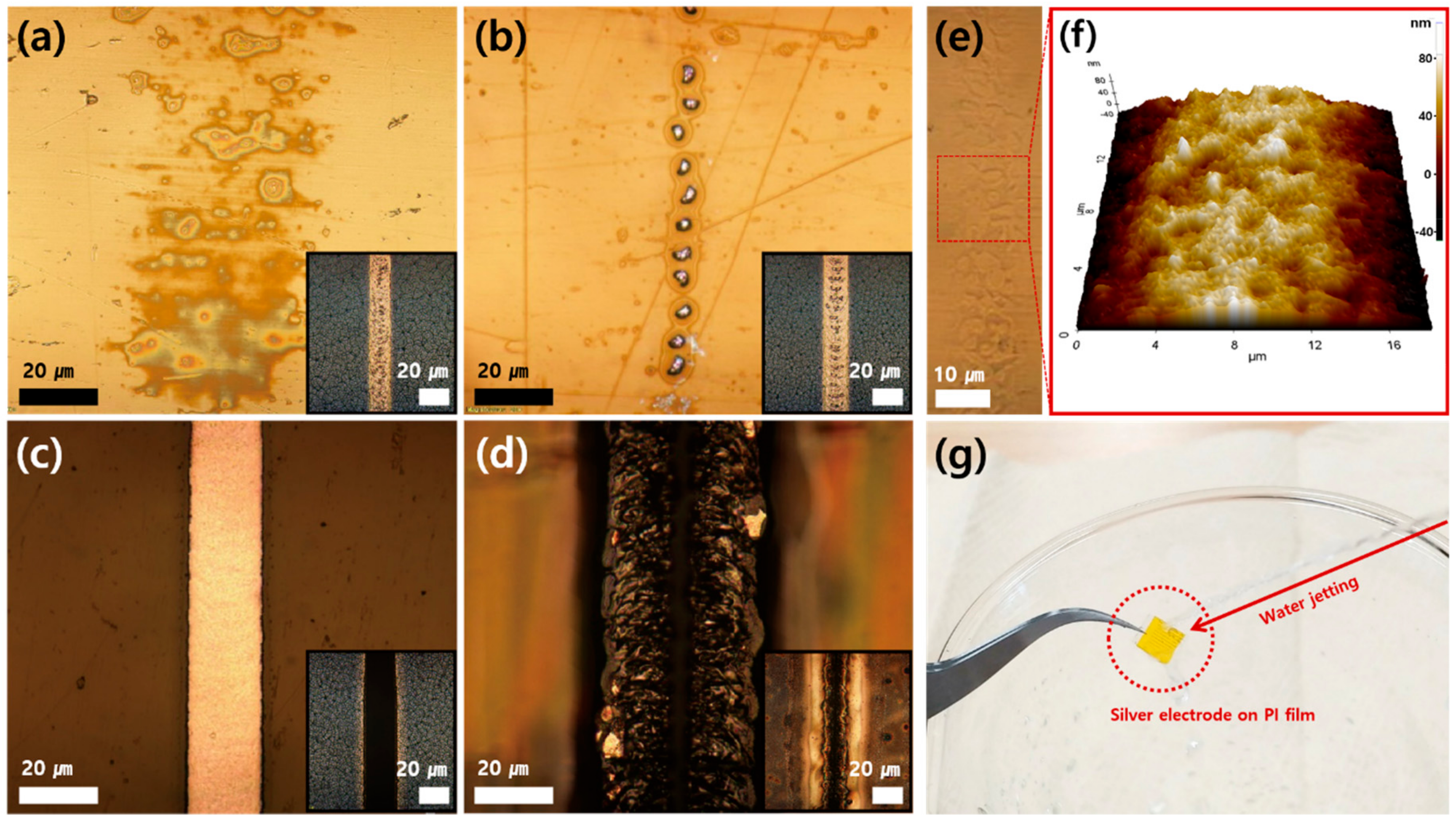
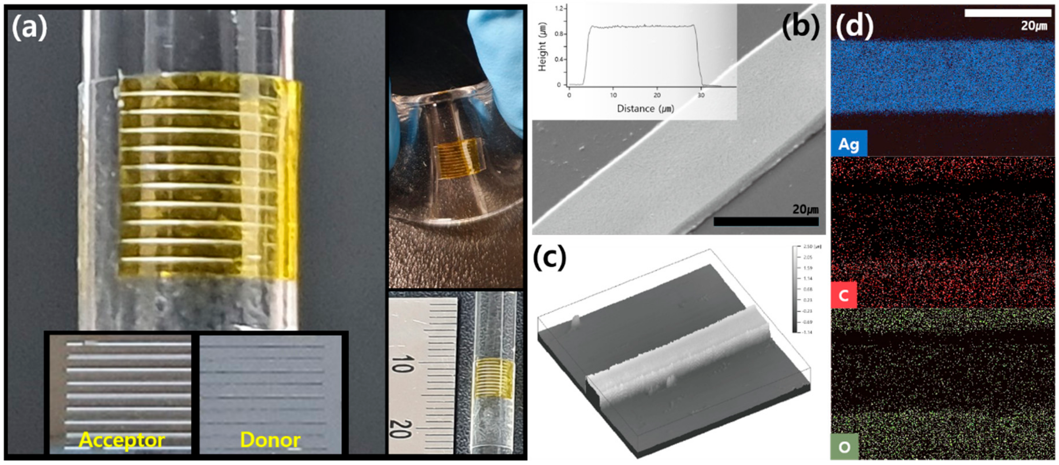
3. Results and Discussion

The proposed method shares common characteristics with the conventional SLS method [9,10], as the laser is utilized to convert the metal NP ink into a continuous conductive layer in a selective manner. At the same time, however, the objective of the current technique is to transfer the resultant conductive layer to the target polymer substrate and the current study should be classified as a laser transfer technique. It is noticeable that the proposed method possesses two differences compared to the conventional LIFT process. First, a pulsed laser is substituted by a CW laser that is more widely available. Secondly, the donor and the acceptor are in direct contact, while the gap distance between the two substrates had to be precisely controlled in the previous studies [17,18]. The experimental configuration is analogous to the shear-assisted laser transfer reported by our group previously [15], however, unlike the thin elastomer substrate, an arbitrary polymer film is not conformally attached to the metal NP layer. As a result, an additional glass substrate was added so that the target polymer substrate and the metal NP layer were sandwiched between two auxiliary glass substrates and directly touching each other.
The transfer characteristics are summarized in Figure 2. Upon successful transfer, we can observe the complementary results between the donor and the acceptor, i.e., a selectively sintered Ag electrode is created on the acceptor PI substrate, while the specific area of the laser-scanned Ag NP layer is removed from the donor glass substrate. Since the amount of the laser-induced heat is the most critical parameter for the features of the resultant, a parametric study was conducted by changing the laser power, while other variables such as the laser wavelength, the magnification of the objective lens and the spin coating condition were fixed. According to the laser power, we classified the transfer feature into four modes (Figure 2a–d). When the laser power is under 200 mW, it is noticeable that the Ag NP is sintered on the donor glass substrate, but there is no notable change on the acceptor PI film. By increasing the laser power to 200–230 mW, irregular patterns appear on the acceptor, while porous holes occur at the sintered Ag electrode on the donor (Figure 2a). We expect that the trapped solvent from the Ag NP ink layer is evaporated by the laser heating and condensed onto the acceptor PI film [17,29], leaving porous holes that originated from the rapid evaporation. Between 230 and 250 mW, regular Ag microparticles are transferred onto the acceptor PI film, while the sintered Ag electrode has complementary micro holes on the surface (Figure 2b). This phenomenon appears to be a typical balling effect [30,31] that is frequently reported in the relevant studies. The formation procedure, relevant factors that affect the results and the mechanism are very complex in the laser-induced balling effect, and since this is often considered as a defect in the typical SLS process, we attempted to find the optimum laser power that suppresses the balling phenomenon, which was experimentally found at 270 mW in this study (Figure 2c). At the optimum condition, a high-quality electrode is created at the acceptor while the Ag NP layer is sharply detached from the donor substrate. When the laser power overpasses 400 mW, the acceptor PI film is pyrolyzed and carbonized [32,33] (Figure 2d) to create a highly uneven structure.
Besides the successful demonstrations above, the stable and smooth transfer of the Ag electrode from the glass to the polymer substrate appears to require a supplementary explanation for its mechanism. We noted the asymmetric adhesion between the electrode and each substrate, and expected to find a reasonable explanation. To further discuss, firstly the adhesion mechanism between the PI substrate and the Ag electrode was investigated. Since it is reasonable to expect the adhesion force originates from the electrode-substrate interface, an investigation of the PI-electrode interface followed. To expose the interface, the Ag electrodes on the PI substrate were removed by chemical etching with a dilute HCl solution. Since PI is well-known for its excellent chemical stability, the removal process could preserve the surface morphology of the interface even after the etching process. Consequently, as shown in Figure 2e, we can identify the irregularities at the position of the removed electrode, which were further revealed as irregular dents and peaks of several micrometers by an AFM measurement (Figure 2f). Considering the intensive laser-thermal energy of focused laser irradiation, the rough surface morphology beneath the electrode could be ascribed to the thermal-deformation of the PI surface driven by the laser irradiation and the resulting thermal energy. Then, such rough topography of the PI surface could provide a plausible explanation for the adhesion at the interface in two ways, as follows. First, from a microscopic point of view, the increased interface area due to the rough topography can greatly enhance the molecular attractive interaction between the PI surface and the Ag electrode. Second, from a macroscopic point of view, the micrometer-sized dents and peaks could induce the mechanical interlocking of each side of the interface. As a result, the adhesion between the PI substrate and the Ag electrode seems to be attributable to the thermal-deformation of the PI substrate surface. On the other hand, the glass, the other side of the Ag electrode, is known to be far more stable to thermal-deformation. The melting point of glass reaches approximately 1500 °C, which exceeds not only the glass transition point of most polymers (~100 °C) but also the authors’ expectation of the laser-induced temperature with the power and scanning values of this study. Therefore, in this case, we could not expect the adhesion mechanism described above, unlike in the case of the PI-electrode interface. Consequently, the above-described thermal deformation induced adhesion mechanism provides a possible explanation for the asymmetric adhesion between the electrode and each substrate. The difference in thermal stability between the PI and the glass substrates generates the asymmetric adhesion that can result in the transfer phenomenon. In addition to the effect of the surface morphology, it is well known that the noble metals do not adhere well to glass [34,35], while the enhanced adhesion between metal and polymer substrate after the SLS process has been experimentally confirmed by numerous studies [9,10]. Meanwhile, enhanced surface adhesion by photothermal reactions has been studied as the driving force of the laser-induced thermal imaging (LITI) method as well [36]. The adhesion of the Ag electrode after the transfer was further tested by jetting water using a squeeze bottle with a nozzle (Figure 2g). It was confirmed that vigorous cleaning using the wash bottle does not result in detachment of the resultant electrode.
Through this proposed method, we could create micro Ag electrodes on the flexible PI film that can be attached to arbitrary irregular shapes such as a cylindrical rod (Figure 3a). For more accurate observation of the created Ag electrode, we measured the transferred Ag electrode with SEM, AFM, an optical surface profiler and EDS (Figure 3b–d). The SEM (Figure 3b) and optical surface profiler (Figure 3c) images show that the selective transfer was achieved on the PI film and also that the transferred Ag electrode has a uniform surface composition. We expect that the simultaneous sintering and transfer processes by the rapid photothermal reaction, together with extremely high temperature gradient, create the Ag electrode without any excessive substances. The AFM measurement (Figure 3b inset) verifies the uniform and flat-top surface of the Ag electrode, and the EDS image (Figure 3d) confirms that the transferred electrode is indeed derived from the Ag NP.
To ensure the electrical conductivity of the resultant, the transferred Ag electrode was connected to power a light-emitting diode (LED). The photographs (Figure 4a) indicate that the Ag electrodes created by the proposed method are available as efficient conductors. From the resistance and the dimensions of the transferred Ag electrode, we obtained a resistivity of 7.243 × 10⁻⁸ Ω·m for the current conductor, which is about five times higher than that of bulk silver (1.59 × 10⁻⁸ Ω·m). This process is directly applicable to other flexible substrates (Figure 4e–g) as shown in the representative examples of the transferred Ag electrode on the polycarbonate (PC) film (Figure 4c), polyethylene terephthalate (PET) film (Figure 4d), thermoplastic polyurethane (TPU) film (Figure 4e), and even on a commercial nitrile glove (Figure 4f) and 3M tape (Figure 4g). For these substrates, the transfer of the Ag electrode occurs effectively at a similar laser power, and we expect that the transferred mechanism is analogous in every case.
As shown in Table 1, the laser-induced transfer method has been mainly studied in the LIFT method using a pulsed laser, which inevitably involves additional heat treatment. There have been several attempts to improve this conventional method. P. Sopeña et al. [23] presented LIFT using a CW laser and secured its possibility as a low-cost fabrication method, but this scheme also requires additional heat treatment because it does not include a simultaneous sintering process. Shin et al. [15] introduced the shear-assisted laser transfer method using a CW laser, which utilizes the thermal expansion coefficient differences between the donor glass substrate and the acceptor Polydimethylsiloxane (PDMS) in conformal contact. However, the shear-assisted laser transfer method requires a substrate with high transparency and thermal expansion coefficients, making it difficult to apply to arbitrary polymer substrates.

4. Conclusions

The laser-induced transfer method of metal NPs using a CW laser, apart from the conventional LIFT method using a pulsed laser, has hardly been developed to date, since the main transfer mechanism has remained as jet formation. The current study reports the micropatterning of the target metal NP onto a flexible acceptor substrate by harnessing the different adhesion strengths that originate from the thermal deformation. Through the proposed process, the sintering and transfer occur simultaneously at a single optical platform without the need for the additional cleaning process. As a result, the proposed method could be an efficient integrated and complementary technique for the previous SLS and LIFT process for metal NPs. We expect that the current study can be applied to a wide range of substrates with enough heat resistance to endure the sintering temperature of the metal NPs. Furthermore, we anticipate that this method is principally material-independent, such that an identical process would be compatible with a variety of metal NPs. The proposed CW laser-induced transfer method, therefore, appears to possess a large potential as a facile manufacturing scheme for flexible electronics.

Author Contributions

S.H., J.L. and W.S. designed the study; J.L. and Y.K. conducted the experiments; J.S., Y.L. and S.P. conducted the measurements; S.H., W.Q. analyzed the data; E.H. assisted the visualization and editing of the manuscript; J.L., Y.K. and S.H. co-wrote the manuscript. All authors have read and agreed to the published version of the manuscript.

Funding

This work was supported by the ‘Human Resources Program in Energy Technology’ of the Korea Institute of Energy Technology Evaluation and Planning (KETEP), and granted financial resource from the Ministry of Trade, Industry & Energy, Republic of Korea (No. 20194010201740) and National Research Foundation of Korea (NRF) Grant funded through the Basic Science Research Program (NRF-2020R1C1C1013503).

Conflicts of Interest

The authors declare no conflict of interest.

References

  1. Kim, J.; Campbell, A.S.; de Avila, B.E.; Wang, J. Wearable biosensors for healthcare monitoring. Nat. Biotechnol. 2019, 37, 389–406. [Google Scholar] [CrossRef]
  2. Bao, Z.; Chen, X. Flexible and Stretchable Devices. Adv. Mater. 2016, 28, 4177–4179. [Google Scholar] [CrossRef] [Green Version]
  3. Liu, Y.; Pharr, M.; Salvatore, G.A. Lab-on-Skin: A Review of Flexible and Stretchable Electronics for Wearable Health Monitoring. ACS Nano 2017, 11, 9614–9635. [Google Scholar] [CrossRef] [PubMed]
  4. Jayathilaka, W.A.D.M.; Qi, K.; Qin, Y.; Chinnappan, A.; Serrano-García, W.; Baskar, C.; Wang, H.; He, J.; Cui, S.; Thomas, S.W.; et al. Significance of Nanomaterials in Wearables: A Review on Wearable Actuators and Sensors. Adv. Mater. 2019, 31, 1805921. [Google Scholar] [CrossRef] [PubMed]
  5. Hong, S.; Lee, H.; Lee, J.; Kwon, J.; Han, S.; Suh, Y.D.; Cho, H.; Shin, J.; Yeo, J.; Ko, S.H. Highly stretchable and transparent metal nanowire heater for wearable electronics applications. Adv. Mater. 2015, 27, 4744–4751. [Google Scholar] [CrossRef]
  6. Perelaer, J.; Schubert, U.S. Novel approaches for low temperature sintering of inkjet-printed inorganic nanoparticles for roll-to-roll (R2R) applications. J. Mater. Res. 2013, 28, 564–573. [Google Scholar] [CrossRef]
  7. Kumpulainen, T.; Pekkanen, J.; Valkama, J.; Laakso, J.; Tuokko, R.; Mäntysalo, M. Low temperature nanoparticle sintering with continuous wave and pulse lasers. Opt. Laser Technol. 2011, 43, 570–576. [Google Scholar] [CrossRef]
  8. Ko, S.H.; Pan, H.; Grigoropoulos, C.P.; Luscombe, C.K.; Fréchet, J.M.J.; Poulikakos, D. All-inkjet-printed flexible electronics fabrication on a polymer substrate by low-temperature high-resolution selective laser sintering of metal nanoparticles. Nanotechnology 2007, 18. [Google Scholar] [CrossRef]
  9. Hong, S.; Yeo, J.; Kim, G.; Kim, D.; Lee, H.; Kwon, J.; Lee, H.; Lee, P.; Ko, S.H. Nonvacuum, Maskless Fabrication of a Flexible Metal Grid Transparent Conductor by Low-Temperature Selective Laser Sintering of Nanoparticle Ink. ACS Nano 2013, 7, 5024–5031. [Google Scholar] [CrossRef]
  10. Yeo, J.; Hong, S.; Lee, D.; Hotz, N.; Lee, M.T.; Grigoropoulos, C.P.; Ko, S.H. Next generation non-vacuum, maskless, low temperature nanoparticle ink laser digital direct metal patterning for a large area flexible electronics. PLoS ONE 2012, 7, e42315. [Google Scholar] [CrossRef] [Green Version]
  11. Kwon, J.; Cho, H.; Eom, H.; Lee, H.; Suh, Y.D.; Moon, H.; Shin, J.; Hong, S.; Ko, S.H. Low-Temperature Oxidation-Free Selective Laser Sintering of Cu Nanoparticle Paste on a Polymer Substrate for the Flexible Touch Panel Applications. Acs Appl. Mater. Interfaces 2016, 8, 11575–11582. [Google Scholar] [CrossRef] [PubMed]
  12. Cheng, C.W.; Chen, J.K. Femtosecond laser sintering of copper nanoparticles. Appl. Phys. A 2016, 122. [Google Scholar] [CrossRef]
  13. Nam, V.B.; Shin, J.; Yoon, Y.; Giang, T.T.; Kwon, J.; Suh, Y.D.; Yeo, J.; Hong, S.; Ko, S.H.; Lee, D. Highly Stable Ni-Based Flexible Transparent Conducting Panels Fabricated by Laser Digital Patterning. Adv. Funct. Mater. 2019, 29. [Google Scholar] [CrossRef]
  14. Shin, J.; Jeong, B.; Kim, J.; Nam, V.B.; Yoon, Y.; Jung, J.; Hong, S.; Lee, H.; Eom, H.; Yeo, J.; et al. Sensitive Wearable Temperature Sensor with Seamless Monolithic Integration. Adv. Mater. 2020, 32, 1905527. [Google Scholar] [CrossRef]
  15. Shin, W.; Lim, J.; Lee, Y.; Park, S.; Kim, H.; Cho, H.; Shin, J.; Yoon, Y.; Lee, H.; Kim, H.J.; et al. Shear-Assisted Laser Transfer of Metal Nanoparticle Ink to an Elastomer Substrate. Materials 2018, 11. [Google Scholar] [CrossRef] [Green Version]
  16. Boesel, L.F. Transfer printing processes. In Generating Micro- and Nanopatterns on Polymeric Materials; del Campo, A., Arzt, E., Eds.; Wiley-VCH: Weinheim, Germany, 2011; pp. 69–92. [Google Scholar] [CrossRef]
  17. Serra, P.; Piqué, A. Laser-Induced Forward Transfer: Fundamentals and Applications. Adv. Mater. Technol. 2019, 4. [Google Scholar] [CrossRef] [Green Version]
  18. Papazoglou, S.; Zergioti, I. Laser Induced Forward Transfer (LIFT) of nano-micro patterns for sensor applications. Microelectron. Eng. 2017, 182, 25–34. [Google Scholar] [CrossRef]
  19. Puerto, D.; Biver, E.; Alloncle, A.P.; Delaporte, P. Single step high-speed printing of continuous silver lines by laser-induced forward transfer. Appl. Surf. Sci. 2016, 374, 183–189. [Google Scholar] [CrossRef]
  20. Florian, C.; Caballero-Lucas, F.; Fernández-Pradas, J.M.; Ogier, S.; Winchester, L.; Karnakis, D.; Geremia, R.; Artigas, R.; Serra, P. Printing of silver conductive lines through laser-induced forward transfer. Appl. Surf. Sci. 2016, 374, 265–270. [Google Scholar] [CrossRef]
  21. Florian, C.; Caballero-Lucas, F.; Fernández-Pradas, J.M.; Artigas, R.; Ogier, S.; Karnakis, D.; Serra, P. Conductive silver ink printing through the laser-induced forward transfer technique. Appl. Surf. Sci. 2015, 336, 304–308. [Google Scholar] [CrossRef]
  22. Fernández-Pradas, J.M.; Sopeña, P.; González-Torres, S.; Arrese, J.; Cirera, A.; Serra, P. Laser-induced forward transfer for printed electronics applications. Appl. Phys. A 2018, 124. [Google Scholar] [CrossRef]
  23. Sopena, P.; Arrese, J.; Gonzalez-Torres, S.; Fernandez-Pradas, J.M.; Cirera, A.; Serra, P. Low-Cost Fabrication of Printed Electronics Devices through Continuous Wave Laser-Induced Forward Transfer. ACS Appl. Mater. Interfaces 2017, 9, 29412–29417. [Google Scholar] [CrossRef] [PubMed]
  24. Sopena, P.; Gonzalez-Torres, S.; Fernandez-Pradas, J.M.; Serra, P. Spraying dynamics in continuous wave laser printing of conductive inks. Sci. Rep. 2018, 8, 7999. [Google Scholar] [CrossRef] [PubMed]
  25. Zacharatos, F.; Theodorakos, I.; Karvounis, P.; Tuohy, S.; Braz, N.; Melamed, S.; Kabla, A.; de la Vega, F.; Andritsos, K.; Hatziapostolou, A.; et al. Selective Laser Sintering of Laser Printed Ag Nanoparticle Micropatterns at High Repetition Rates. Materials 2018, 11, 2142. [Google Scholar] [CrossRef] [PubMed] [Green Version]
  26. Jalaal, M.; Li, S.; Klein Schaarsberg, M.; Qin, Y.; Lohse, D. Destructive mechanisms in laser induced forward transfer. Appl. Phys. Lett. 2019, 114, 213703. [Google Scholar] [CrossRef]
  27. Mathews, S.A.; Auyeung, R.C.Y.; Kim, H.; Charipar, N.A.; Piqué, A. High-speed video study of laser-induced forward transfer of silver nano-suspensions. J. Appl. Phys. 2013, 114. [Google Scholar] [CrossRef]
  28. Park, S.; Kwon, J.; Lim, J.; Shin, W.; Lee, Y.; Lee, H.; Kim, H.J.; Han, S.; Yeo, J.; Ko, S.H.; et al. Micropatterning of Metal Nanoparticle Ink by Laser-Induced Thermocapillary Flow. Nanomaterials 2018, 8, 645. [Google Scholar] [CrossRef] [Green Version]
  29. Raynor, P.C.; Leith, D. Evaporation of accumulated multicomponent liquids from fibrous filters. Ann. Occup. Hyg. 1999, 43, 181–192. [Google Scholar] [CrossRef]
  30. Shen, Y.F.; Gu, D.D.; Pan, Y.F. Balling Process in Selective Laser Sintering 316 Stainless Steel Powder. Key Eng. Mater. 2006, 315–316, 357–360. [Google Scholar] [CrossRef]
  31. Oyar, P. Laser Sintering Technology and Balling Phenomenon. Photomed. Laser Surg. 2018, 36, 72–77. [Google Scholar] [CrossRef]
  32. Tiliakos, A.; Ceaus, C.; Iordache, S.M.; Vasile, E.; Stamatin, I. Morphic transitions of nanocarbons via laser pyrolysis of polyimide films. J. Anal. Appl. Pyrolysis 2016, 121, 275–286. [Google Scholar] [CrossRef]
  33. Mamleyev, E.R.; Heissler, S.; Nefedov, A.; Weidler, P.G.; Nordin, N.; Kudryashov, V.V.; Länge, K.; MacKinnon, N.; Sharma, S. Laser-induced hierarchical carbon patterns on polyimide substrates for flexible urea sensors. NPJ Flex. Electron. 2019, 3, 2. [Google Scholar] [CrossRef]
  34. Lee, LH. (Ed.) The chemistry and physics of solid adhesion. In Fundamentals of Adhesion; Springer: Boston, MA, USA, 1991; pp. 1–86. [Google Scholar] [CrossRef]
  35. Benjamin, P.; Weaver, C.; Mott, N.F. The adhesion of evaporated metal films on glass. Proc. R. Soc. Lond. Ser. A Math. Phys. Sci. 1961, 261, 516–531. [Google Scholar] [CrossRef]
  36. Blanchet, G.B.; Loo, Y.-L.; Rogers, J.A.; Gao, F.; Fincher, C.R. Large area, high resolution, dry printing of conducting polymers for organic electronics. Appl. Phys. Lett. 2003, 82, 463–465. [Google Scholar] [CrossRef] [Green Version]
  37. Makrygianni, M.; Kalpyris, I.; Boutopoulos, C.; Zergioti, I. Laser induced forward transfer of Ag nanoparticles ink deposition and characterization. Appl. Surf. Sci. 2014, 297, 40–44. [Google Scholar] [CrossRef]
  38. Sopena, P.; Fernández-Pradas, J.M.; Serra, P. Laser-induced forward transfer of low viscosity inks. Appl. Surf. Sci. 2017, 418, 530–535. [Google Scholar] [CrossRef]
  39. Theodorakos, I.; Kalaitzis, A.; Makrygianni, M.; Hatziapostolou, A.; Kabla, A.; Melamed, S.; de la Vega, F.; Zergioti, I. Laser-Induced Forward Transfer of High Viscous, Non-Newtonian Silver Nanoparticle Inks: Jet Dynamics and Temporal Evolution of the Printed Droplet Study. Adv. Eng. Mater. 2019, 21. [Google Scholar] [CrossRef] [Green Version]
  40. Koritsoglou, O.; Theodorakos, I.; Zacharatos, F.; Makrygianni, M.; Kariyapperuma, D.; Price, R.; Cobb, B.; Melamed, S.; Kabla, A.; de la Vega, F.; et al. Copper micro-electrode fabrication using laser printing and laser sintering processes for on-chip antennas on flexible integrated circuits. Opt. Mater. Express 2019, 9, 3046–3058. [Google Scholar] [CrossRef]
  41. Wang, X.S.; Xu, B.; Huang, Y.K.; Zhang, J.; Liu, Q. Laser-induced forward transfer of silver nanoparticle ink using burst technique. Appl. Phys. A Mater. 2019, 125, 845. [Google Scholar] [CrossRef]
Figure 1. Schematics of the CW laser-induced Ag NP transfer to the thin polymer film. (a) Spin coating of the Ag NP ink onto the donor glass substrate. (b) Laser scanning conducted at the Ag NP layer, which is sandwiched between the glass substrate and the polymer film. (c) The detachment of the donor substrate with the Ag NP. (d) Ag electrode on the acceptor polymer film transferred from the donor substrate.
Nanomaterials 10 00701 g001
Figure 2. Parametric studies seeking the optimum laser parameters. Optical microscope images of the acceptor according to the laser power (laser velocity was fixed at 5 mm/s); (a) 210 mW, (b) 240 mW (c) 270 mW and (d) 400 mW (inset: corresponding donor substrate). (e) Optical and (f) AFM images of the PI film after etching the transferred Ag electrode. (g) Adhesion test against water-jetting.
Nanomaterials 10 00701 g002
Figure 3. (a) Photographs of the transferred Ag electrodes on non-flat substrates such as a cylindrical rod and a bent elastomer (inset: photograph of the acceptor and the donor together with a scale to check the size). (b) SEM (inset: AFM), (c) optical surface profiler and (d) EDS measurements of the transferred Ag electrode.
Nanomaterials 10 00701 g003
Figure 4. (a) Photographs of the circuit using the transferred Ag electrode on the PI film. (b) I-V characteristics of the transferred Ag electrode. Ag electrode transferred to (c) PC film, (d) PET film, (e) TPU film, (f) Nitrile glove and (g) 3M tape. The insets of (cg) are the optical microscope images of the corresponding Ag electrodes.
Nanomaterials 10 00701 g004
Table 1. Recent progress in the laser-induced transfer of metal NPs.
LaserLaser
Condition
DonorAcceptorGap distanceYearMaterialMethodRef.
1Pulsed laser (ns)266 nm
40–100 mJ/cm2
QuartzSiO2300 µm2014SilverLIFT
Additional Heat treatment
[37]
2Pulsed laser (fs)1027 nm
530 mJ/cm2
GlassGlass200 µm2015SilverLIFT
Additional Heat treatment
[21]
3Pulsed laser (fs)1027 nm
530 mJ/cm2
GlassGlass with ablated channel160 µm2016SilverLIFT
Additional Heat treatment
[20]
4Pulsed laser (ps)343 nm
35–64 mJ/cm2
QuartzGlass230 µm2016SilverLIFT
Additional Heat treatment
[19]
5Pulsed laser (ns)1064 nm
2–6 J/cm2
GlassGlass150 µm2017SilverLIFT[38]
6Continuous wave laser1064 nm
1W
600mm/s
GlassGlass150 µm2017SilverCW-LIFT
Additional Heat treatment
[23]
7Pulsed laser (ns)1064 nm
11000 mJ/cm2
GlassPaper150 µm2018SilverLIFT
Additional Heat treatment
[22]
8Continuous wave laser532 nm
0.54 W
140 mm/s
GlassPDMSContact2018SilverShear-assisted[15]
9Pulsed laser (ns)532 nm
320 mJ/cm2
GlassGlass
SU-8 film
Organic layer
150 µm
500 µm
3000 µm
2019SilverLIFT
Additional Heat treatment
[39]
10Pulsed laser (ns)532 nm
360 mJ/cm2
QuartzSU8 on glass100 µm2019CopperLIFT
Post sintering
[40]
11Pulsed laser (ps)532 nm
80–240 nJ
(burst mode)
GlassGlass200 µm2019SilverLIFT(burst)[41]
Current StudyContinuous wave laser532 nm
0.27 W
5 mm/s
GlassPolymer SubstratesContact SilverEnhanced adhesion by CW laser

