Effects of 5 MeV Proton Irradiation on Nitrided SiO2/4H-SiC MOS Capacitors and the Related Mechanisms

 ,
,
Abstract
:1. Introduction
2. Experiments
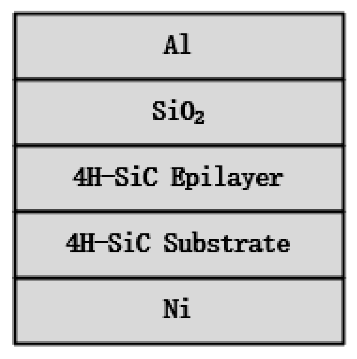
2.1. Test Devices
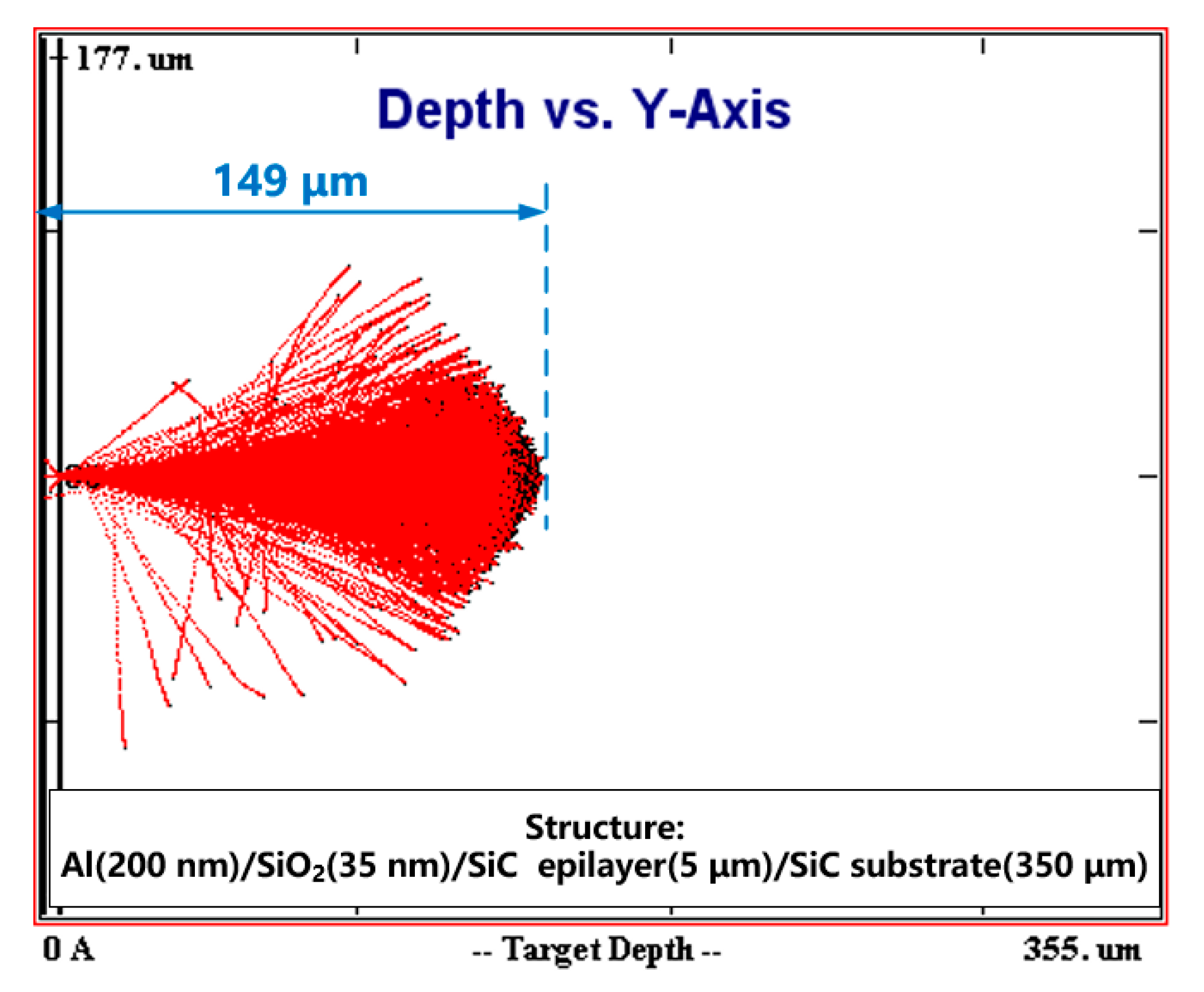
2.2. High Energy Proton Irradiation
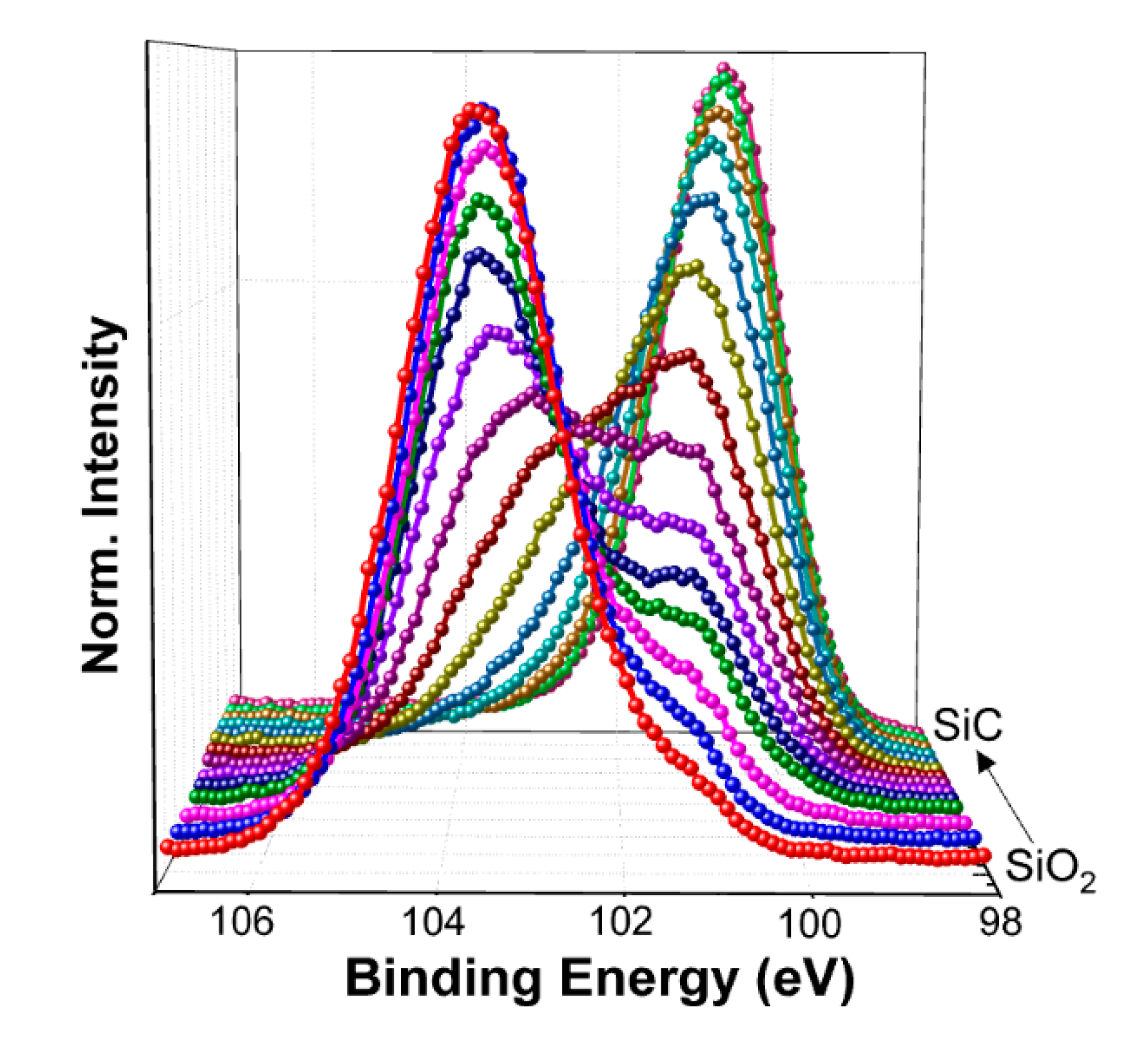
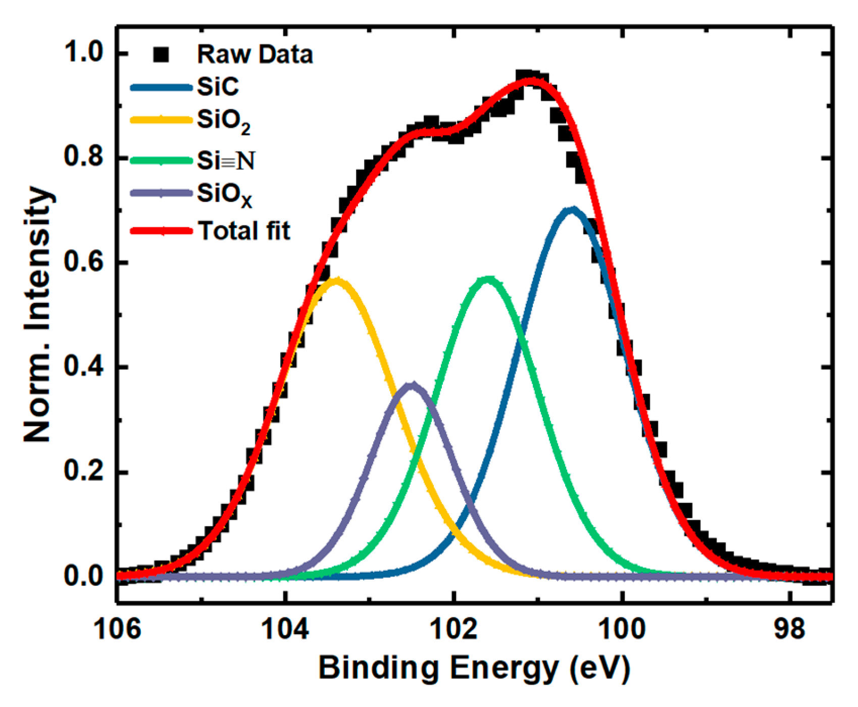
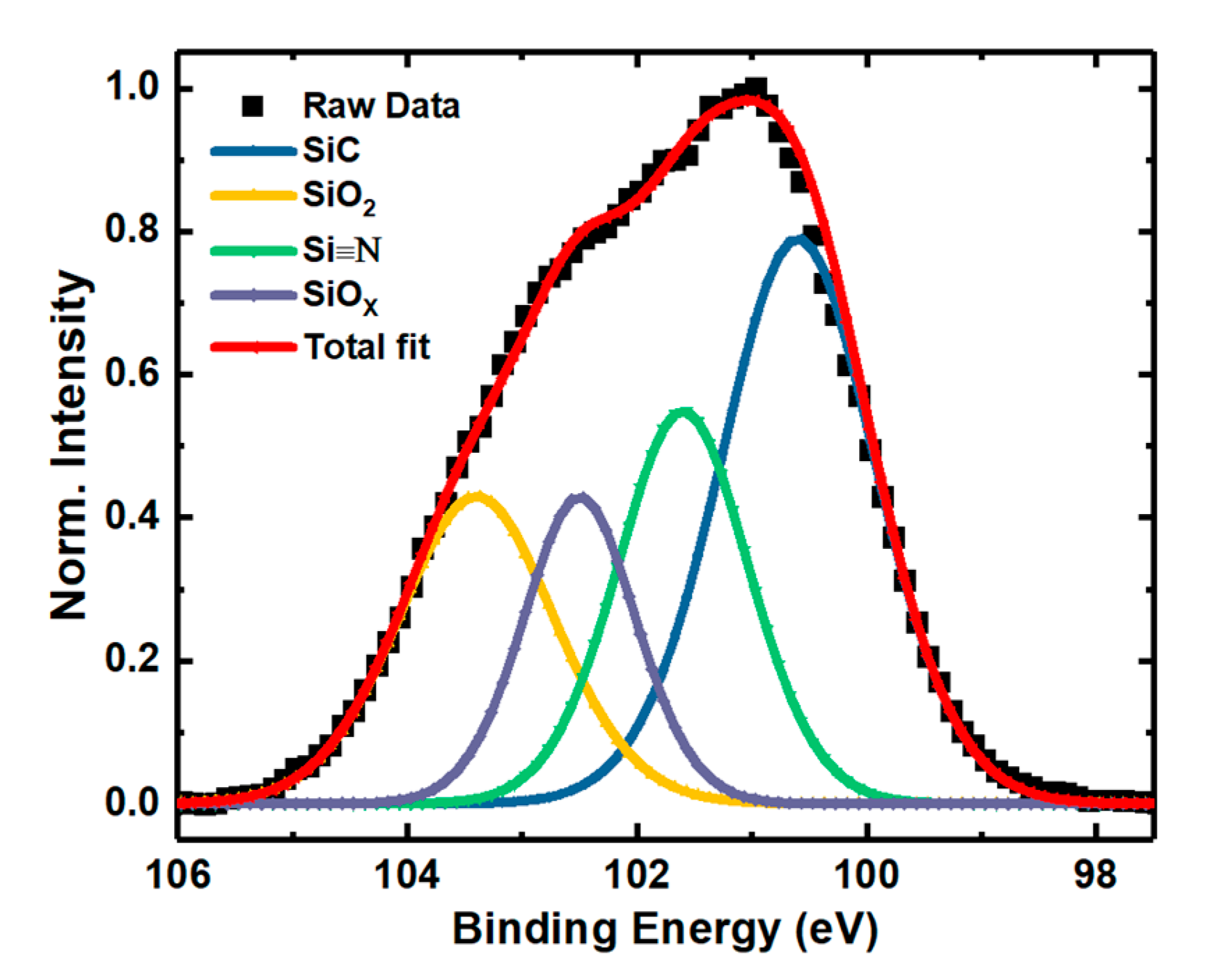
2.3. XPS Measurement and Annealing Experiment
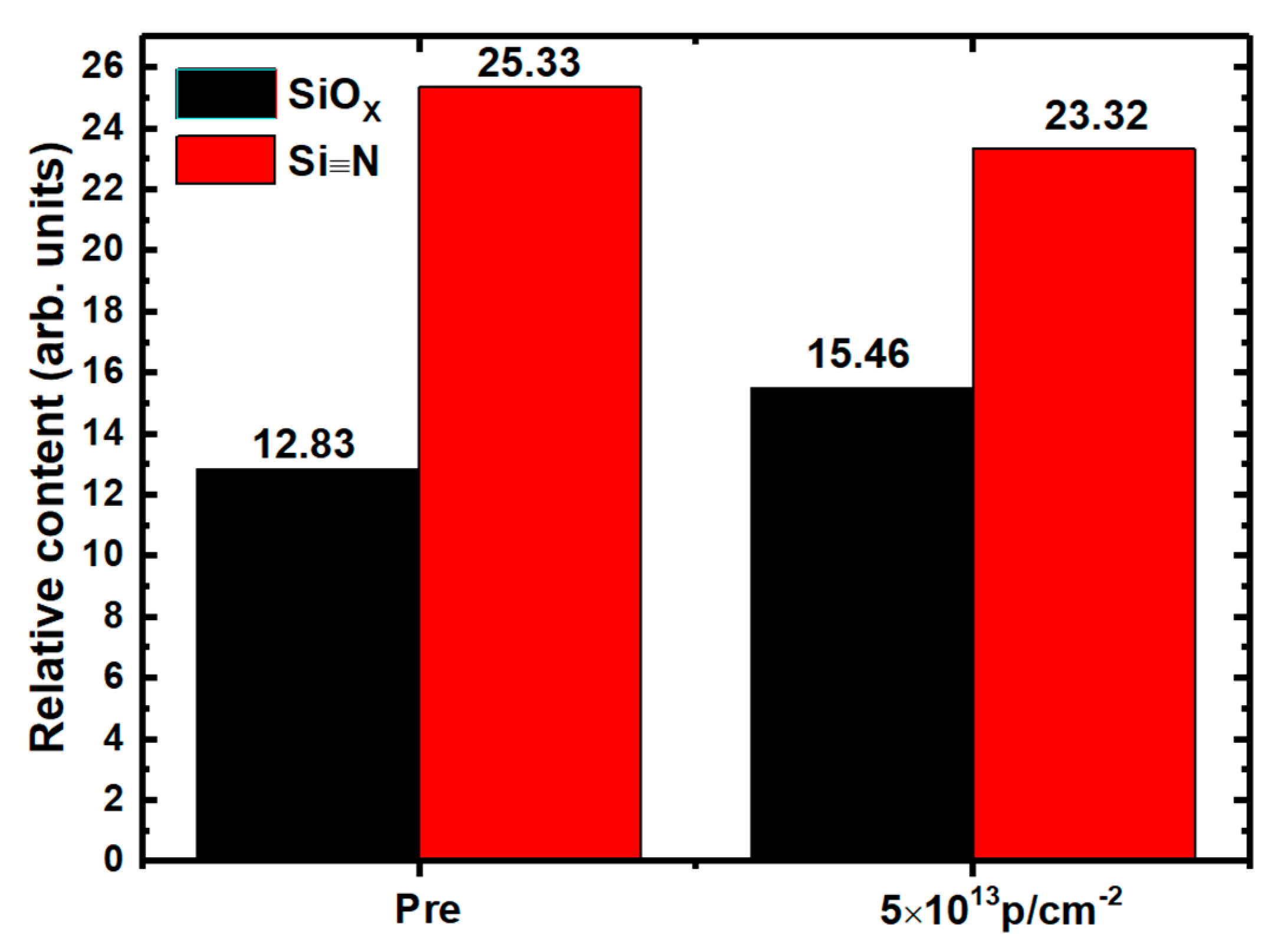
3. Results and Discussion
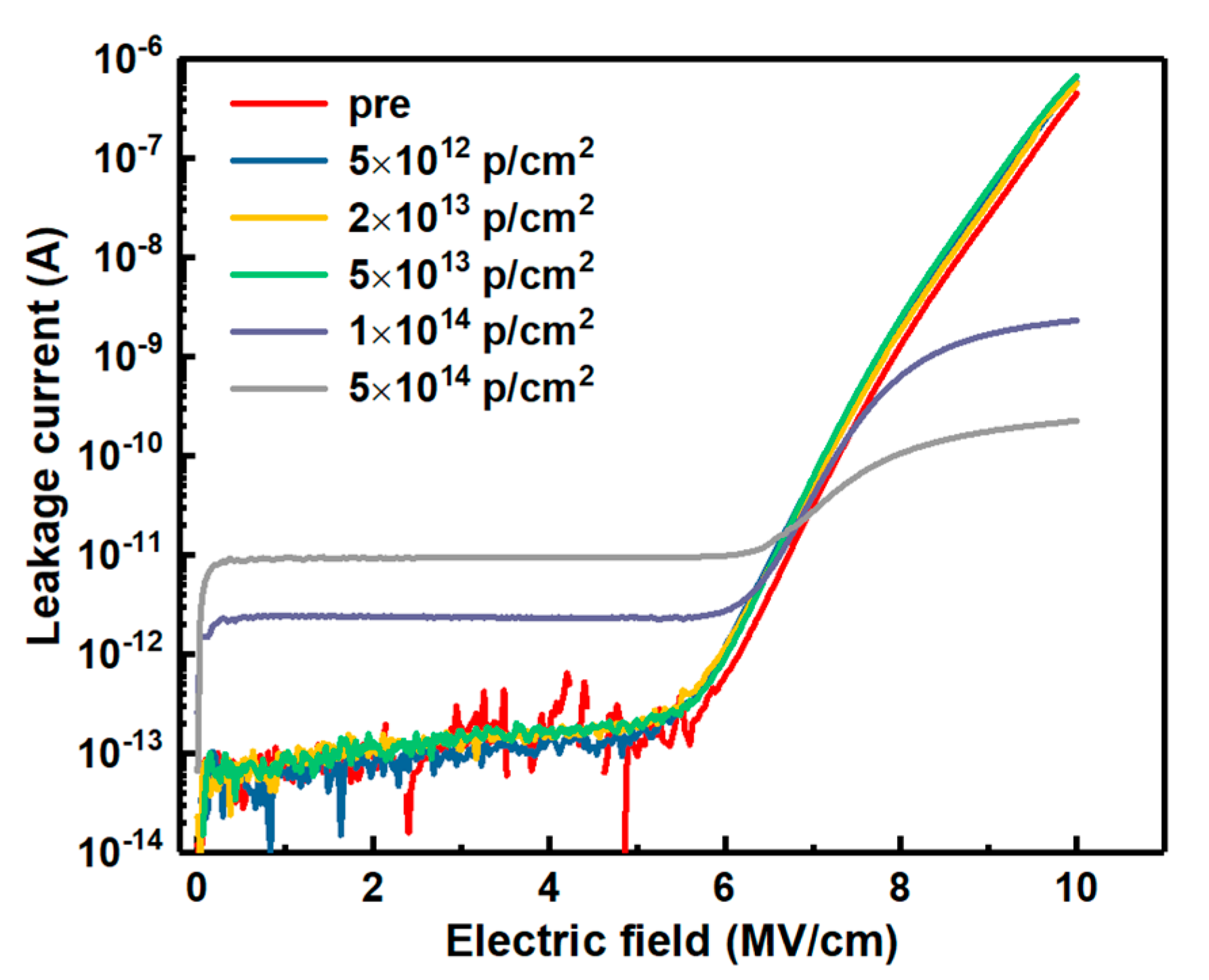
3.1. Gate Oxide Integrity
3.2. Free Carrier Concentration
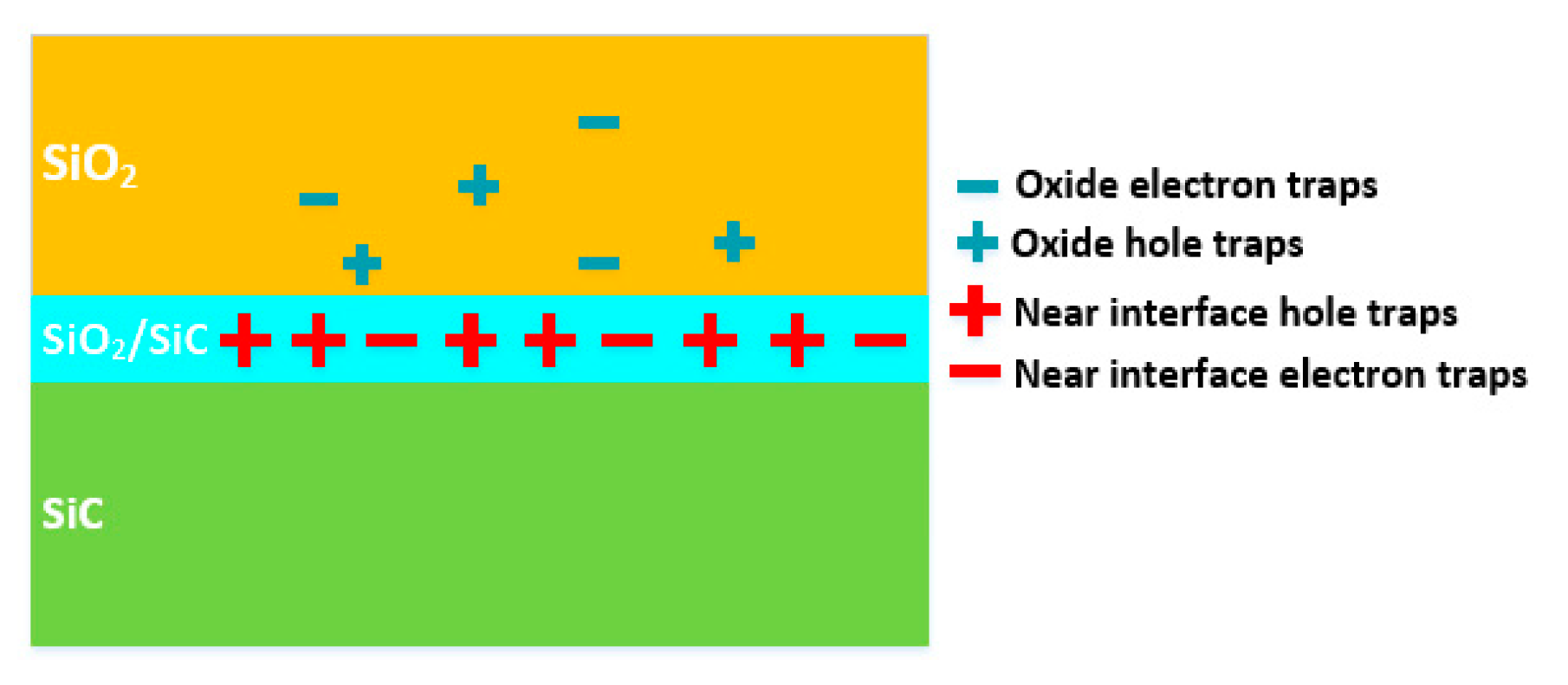
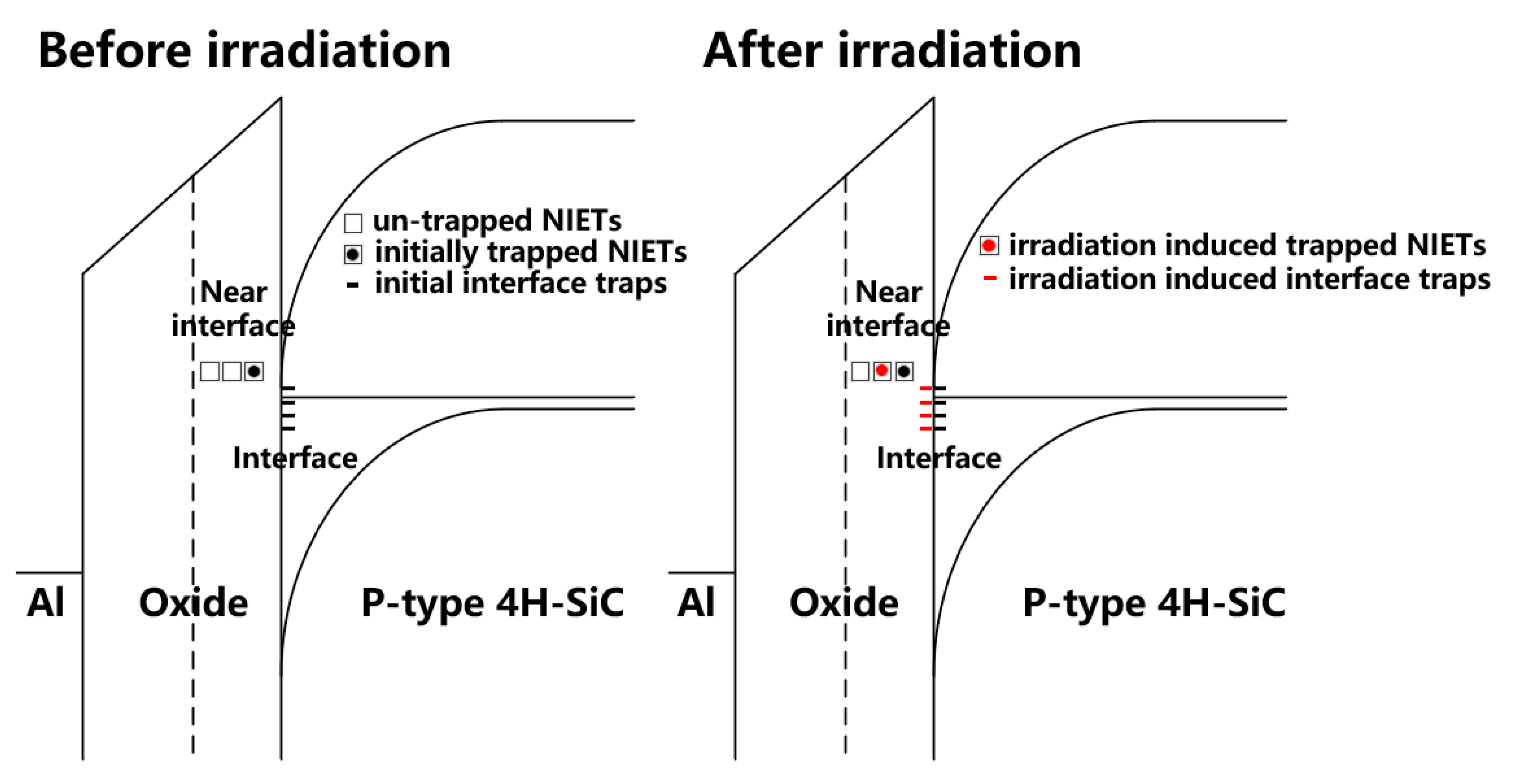
3.3. Near Interface Traps
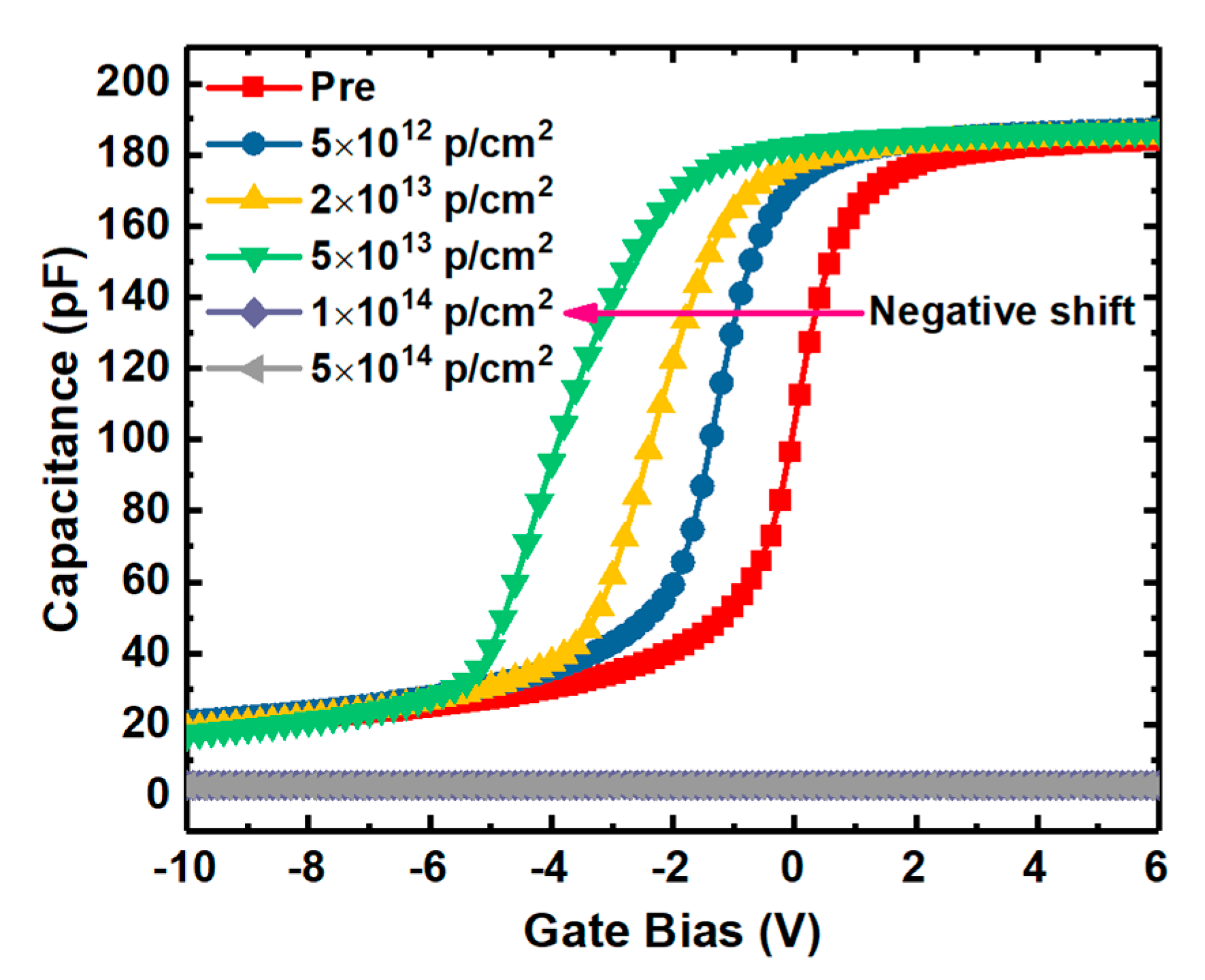
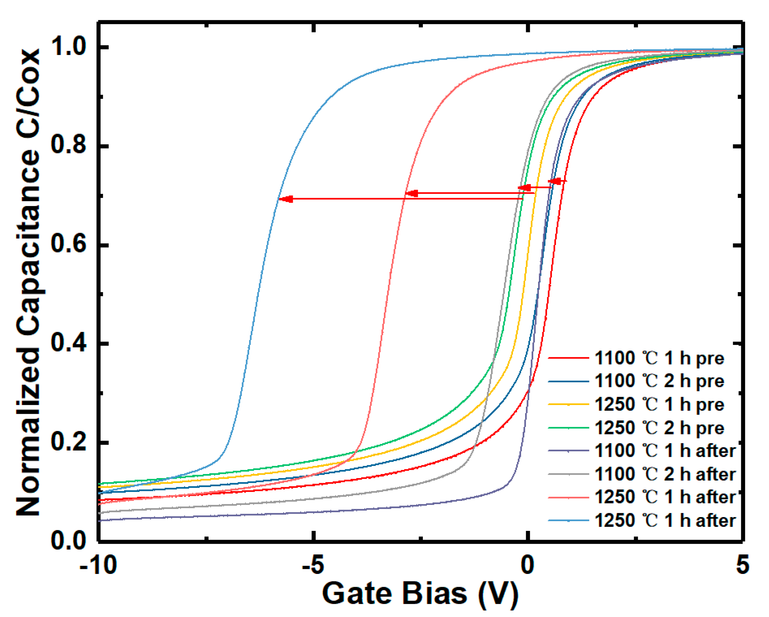
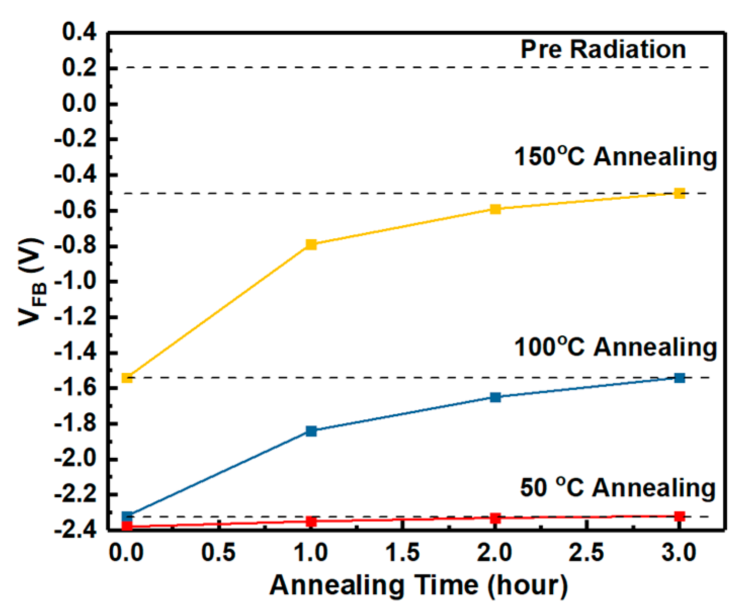
3.4. Flat-Band Voltage
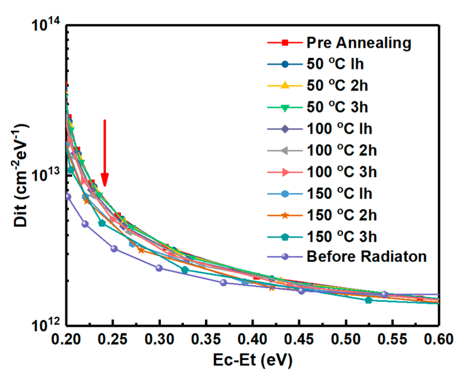
3.5. Interface Traps
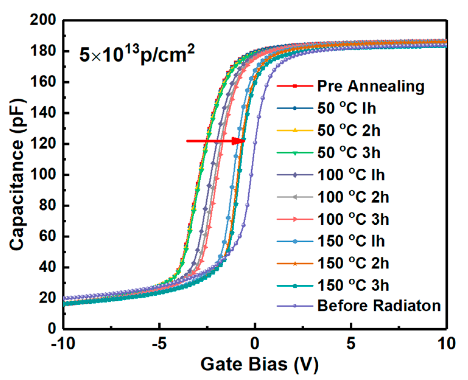
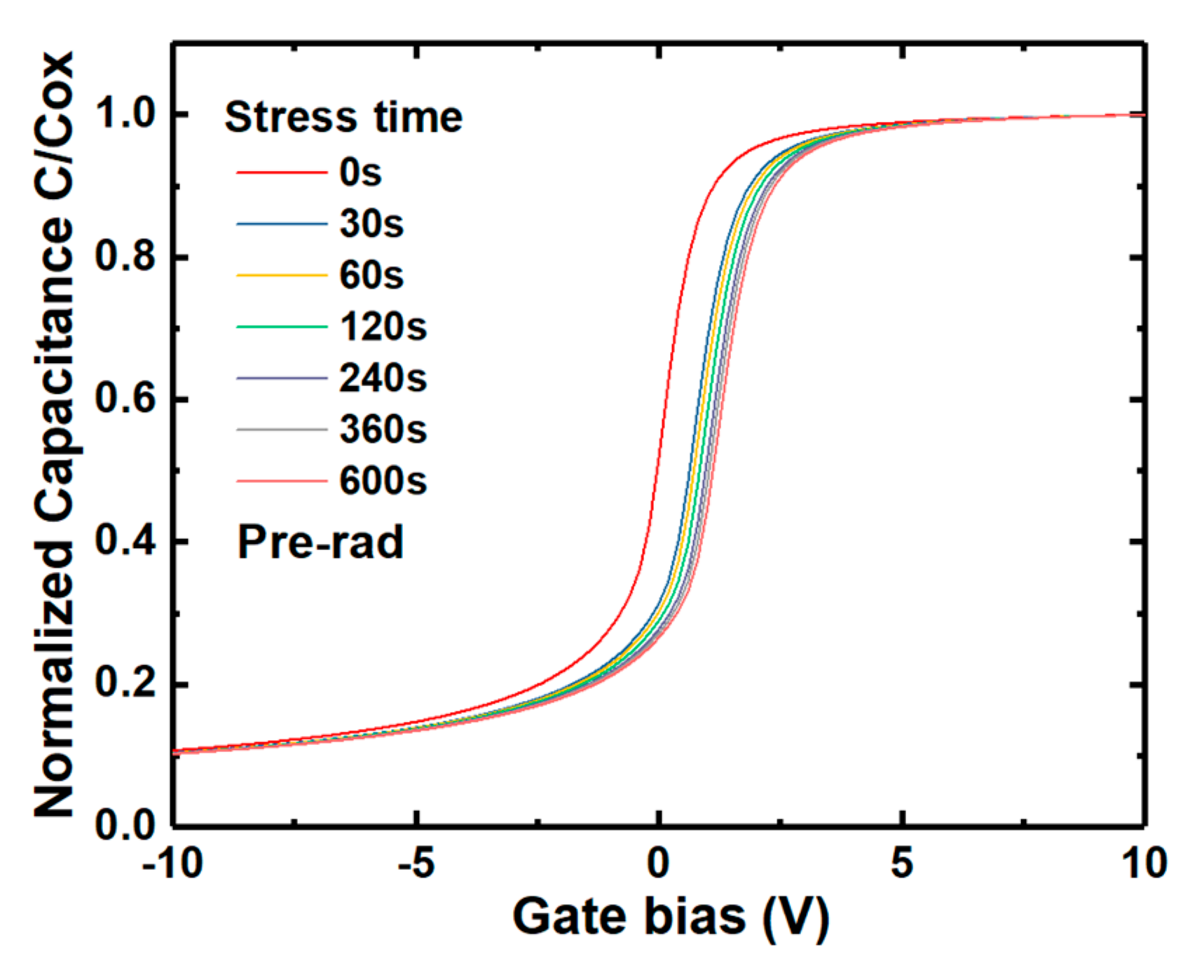
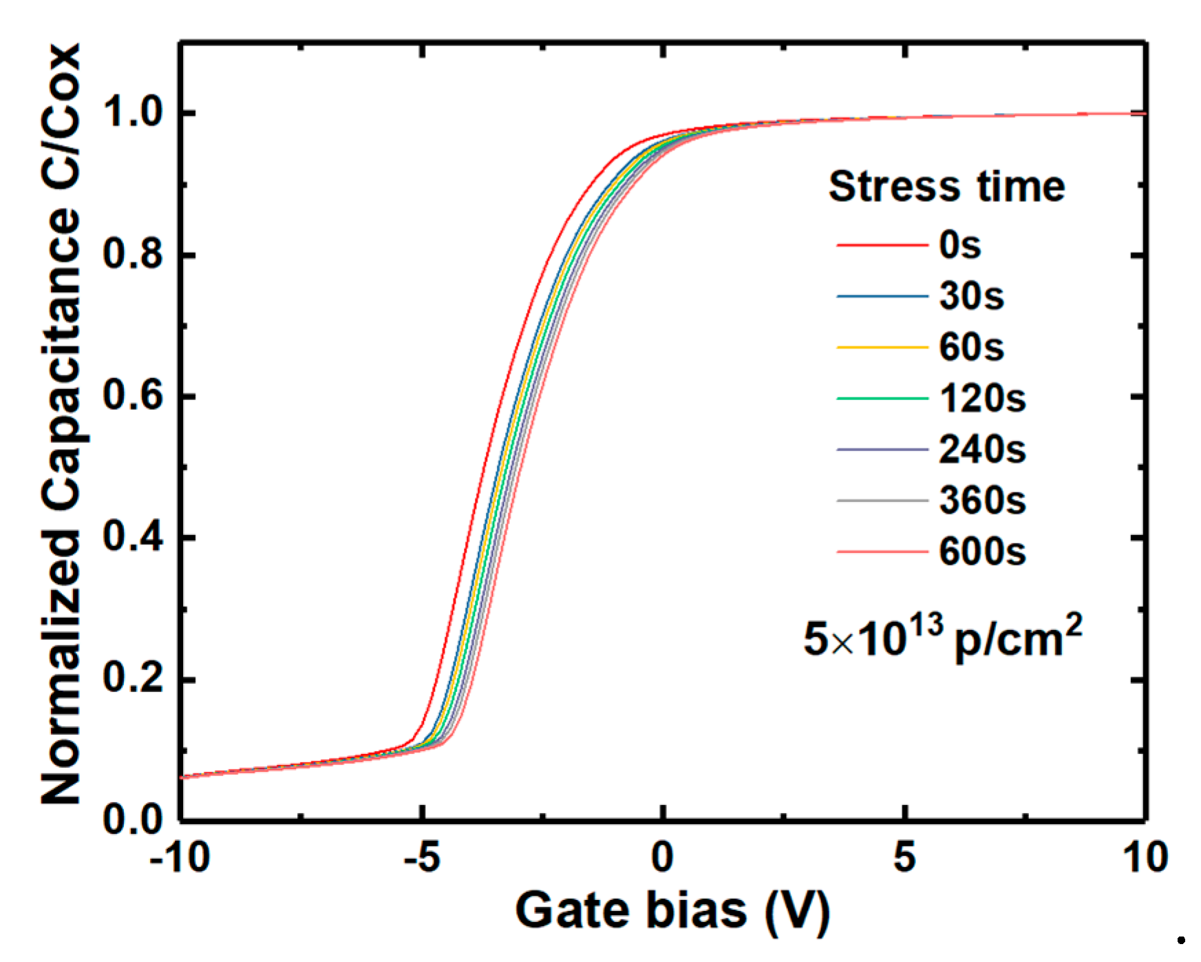
3.6. The Positive Bias Stress Stability of VFB
4. Conclusions
Author Contributions
Funding
Conflicts of Interest
References
- Cooper, J.A.; Agarwal, A. SiC power-switching devices-the second electronics revolution? Proc. IEEE 2002, 90, 956–968. [Google Scholar] [CrossRef]
- Cooper, J.A.; Melloch, M.R.; Singh, R.; Agarwal, A.; Palmour, J.W. Status and prospects for SiC power MOSFETs. IEEE Trans. Electron Devices 2002, 49, 658–664. [Google Scholar] [CrossRef]
- Dixit, S.K.; Dhar, S.; Rozen, J.; Wang, S.; Schrimpf, R.D.; Fleetwood, D.M.; Pantelides, S.T.; Williams, J.R.; Feldman, L.C. Total dose radiation response of nitrided and non-nitrided SiO2/4H-SiC MOS capacitors. IEEE Trans. Nucl. Sci. 2006, 53, 3687–3692. [Google Scholar] [CrossRef]
- Arora, R.; Rozen, J.; Fleetwood, D.M.; Galloway, K.F.; Zhang, C.X.; Han, J.; Dimitrijev, S.; Kong, F.; Feldman, L.C.; Pantelides, S.T.; et al. Charge trapping properties of 3C- and 4H-SiC MOS capacitors with nitrided gate oxides. IEEE Trans. Nucl. Sci. 2009, 56, 3185–3191. [Google Scholar] [CrossRef] [Green Version]
- Zhang, C.X.; Zhang, E.X.; Fleetwood, D.M.; Schrimpf, R.D.; Dhar, S.; Ryu, S.; Shen, X.; Pantelides, S.T. Effects of bias on the irradiation and annealing responses of 4H-SiC MOS devices. IEEE Trans. Nucl. Sci. 2011, 58, 2925–2929. [Google Scholar] [CrossRef]
- Akturk, A.; McGarrity, J.M.; Potbhare, S.; Goldsman, N. Radiation effects in commercial 1200 V 24 A silicon carbide power MOSFETs. IEEE Trans. Nucl. Sci. 2012, 59, 3258–3264. [Google Scholar] [CrossRef]
- Green, R.; Lelis, A.J.; Urciuoli, D.P.; Litz, M.; Carroll, J. Radiation-Induced trapped charging effects in SiC power MOSFETs. Mater. Sci. Forum 2014, 778–780, 533–536. [Google Scholar] [CrossRef]
- Murata, K.; Mitomo, S.; Matsuda, T.; Yokoseki, T.; Makino, T.; Onoda, S.; Takeyama, A.; Ohshima, T.; Okubo, S.; Tanaka, Y.; et al. Impacts of gate bias and its variation on gamma-ray irradiation resistance of SiC MOSFETs. Physica Status Solidi (a) 2017, 214, 1600446. [Google Scholar] [CrossRef]
- Hu, D.; Zhang, J.; Jia, Y.; Wu, Y.; Peng, L.; Tang, Y. Impact of different gate biases on irradiation and annealing responses of SiC MOSFETs. IEEE Trans. Electron Devices 2018, 65, 3719–3724. [Google Scholar] [CrossRef]
- Takeyama, A.; Makino, T.; Okubo, S.; Tanaka, Y.; Yoshie, T.; Hijikata, Y.; Ohshima, T. Radiation Response of Negative Gate Biased SiC MOSFETs. Materials 2019, 12, 2741. [Google Scholar] [CrossRef] [Green Version]
- Alexandru, M.; Florentin, M.; Constant, A.; Schmidt, B.; Michel, P.; Godignon, P. 5 MeV proton and 15 MeV electron radiation effects study on 4H-SiC nMOSFET electrical parameters. IEEE Trans. Nucl. Sci. 2014, 61, 1732–1738. [Google Scholar] [CrossRef]
- Castaldini, A.; Cavallini, A.; Rigutti, L.; Nava, F.; Ferrero, S.; Giorgis, F. Deep levels by proton and electron irradiation in 4H–SiC. J. Appl. Phys. 2005, 98, 053706. [Google Scholar] [CrossRef]
- Stoller, R.E.; Toloczko, M.B.; Was, G.S.; Certain, A.G.; Dwaraknath, S.; Garner, F.A. On the use of SRIM for computing radiation damage exposure. Nucl. Instrum. Methods Phys. Res. Sect. B: Beam Interact. Mater. At. 2013, 310, 75–80. [Google Scholar] [CrossRef]
- Danchenko, V.; Desai, U.D.; Brashears, S.S. Characteristics of thermal annealing of radiation damage in MOSFET’s. J. Appl. Phys. 1968, 39, 2417–2424. [Google Scholar] [CrossRef]
- Jia, Y.; Lv, H.; Song, Q.; Tang, X.; Xiao, L.; Wang, L.; Tang, G.; Zhang, Y.; Zhang, Y. Influence of oxidation temperature on the interfacial properties of n-type 4H-SiC MOS capacitors. Appl. Surf. Sci. 2017, 397, 175–182. [Google Scholar] [CrossRef] [Green Version]
- Pantelides, S.T.; Wang, S.; Franceschetti, A.; Buczko, R.; Di Ventra, M.; Rashkeev, S.N.; Tsetseris, L.; Evans, M.H.; Batyrev, I.G.; Feldman, L.C.; et al. Si/SiO2 and SiC/SiO2 interfaces for MOSFETs—Challenges and advances. Mater. Sci. Forum 2006, 527–529, 935–948. [Google Scholar] [CrossRef]
- Rozen, J.; Dhar, S.; Dixit, S.K.; Afanas’ev, V.V.; Roberts, F.O.; Dang, H.L.; Wang, S.; Pantelides, S.T.; Williams, J.R.; Feldman, L.C. Increase in oxide hole trap density associated with nitrogen incorporation at the SiO2/SiC interface. J. Appl. Phys. 2008, 103, 124513. [Google Scholar] [CrossRef]
- Rozen, J.; Dhar, S.; Zvanut, M.E.; Williams, J.R.; Feldman, L.C. Density of interface states, electron traps, and hole traps as a function of the nitrogen density in SiO2 on SiC. J. Appl. Phys. 2009, 105, 124506. [Google Scholar] [CrossRef]
- Schomer, R.; Friedrichs, P.; Peters, D.; Stephani, D. Significantly improved performance of MOSFETs on silicon carbide using the 15R-SiC polytype. IEEE Electron Device Lett. 1999, 20, 241–244. [Google Scholar] [CrossRef]
- Saks, N.S.; Agarwal, A.K. Hall mobility and free electron density at the SiC/SiO2 interface in 4H–SiC. Appl. Phys. Lett. 2000, 77, 3281–3283. [Google Scholar] [CrossRef]
- Haasmann, D.; Dimitrijev, S. Energy position of the active near-interface traps in metal–oxide–semiconductor field-effect transistors on 4H–SiC. Appl. Phys. Lett. 2013, 103, 113506. [Google Scholar] [CrossRef] [Green Version]
- Jia, Y.; Lv, H.; Niu, Y.; Li, L.; Song, Q.; Tang, X.; Li, C.; Zhao, Y.; Xiao, L.; Wang, L.; et al. Effect of NO annealing on charge traps in oxide insulator and transition layer for 4H-SiC metal–oxide–semiconductor devices. Chin. Phys. B 2016, 25, 097101. [Google Scholar] [CrossRef]


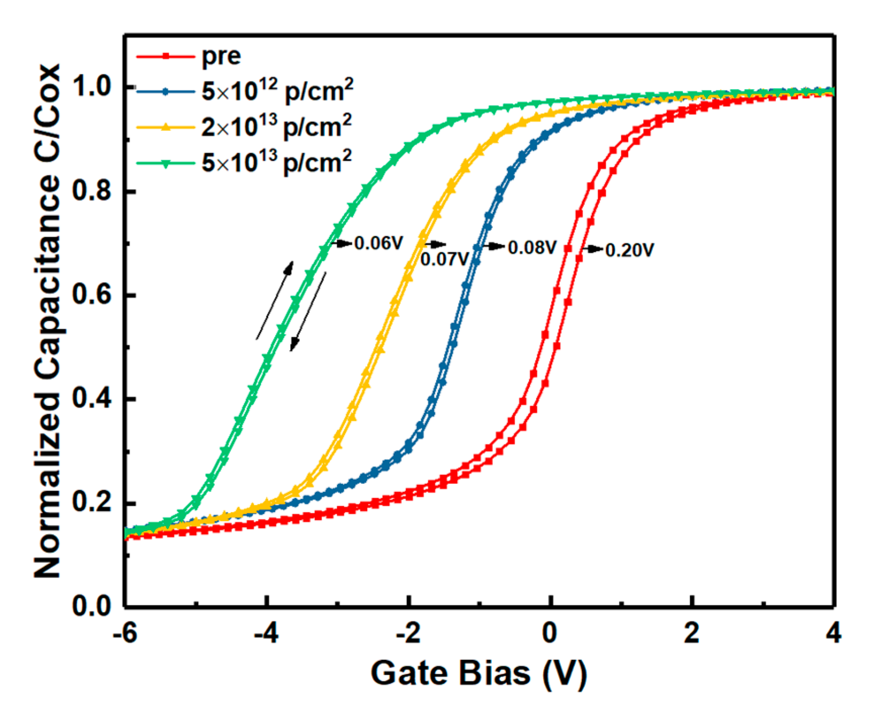
| Irradiation Dose (p/cm2) | Hysteresis Voltage (V) | Areal Density of un-Trapped NIETs (cm−2) |
|---|---|---|
| pre | 0.20 | 1.2 × 10¹¹ |
| 5 × 10¹² | 0.08 | 4.7 × 10¹⁰ |
| 2 × 10¹³ | 0.07 | 4.2 × 10¹⁰ |
| 5 × 10¹³ | 0.06 | 3.6 × 10¹⁰ |
| Annealing Condition | the Shift of VFB (V) | Tox (nm) | ∆Nef (cm−2) |
|---|---|---|---|
| 1100 °C 1 h | 0.3 | 48.0 | 1.4 × 10¹¹ |
| 1100 °C 2 h | 0.9 | 48.8 | 4.0 × 10¹¹ |
| 1250 °C 1 h | 3.2 | 52.8 | 1.3 × 10¹² |
| 1250 °C 2 h | 5.9 | 56.8 | 2.2 × 10¹² |
© 2020 by the authors. Licensee MDPI, Basel, Switzerland. This article is an open access article distributed under the terms and conditions of the Creative Commons Attribution (CC BY) license (http://creativecommons.org/licenses/by/4.0/).
Share and Cite
Li, D.; Zhang, Y.; Tang, X.; He, Y.; Yuan, H.; Jia, Y.; Song, Q.; Zhang, M.; Zhang, Y. Effects of 5 MeV Proton Irradiation on Nitrided SiO2/4H-SiC MOS Capacitors and the Related Mechanisms. Nanomaterials 2020, 10, 1332. https://doi.org/10.3390/nano10071332
Li D, Zhang Y, Tang X, He Y, Yuan H, Jia Y, Song Q, Zhang M, Zhang Y. Effects of 5 MeV Proton Irradiation on Nitrided SiO2/4H-SiC MOS Capacitors and the Related Mechanisms. Nanomaterials. 2020; 10(7):1332. https://doi.org/10.3390/nano10071332
Chicago/Turabian StyleLi, Dongxun, Yuming Zhang, Xiaoyan Tang, Yanjing He, Hao Yuan, Yifan Jia, Qingwen Song, Ming Zhang, and Yimen Zhang. 2020. "Effects of 5 MeV Proton Irradiation on Nitrided SiO2/4H-SiC MOS Capacitors and the Related Mechanisms" Nanomaterials 10, no. 7: 1332. https://doi.org/10.3390/nano10071332