
MoTe2 Field-Effect Transistors with Low Contact Resistance through Phase Tuning by Laser Irradiation


1
Green and Sustainable Materials R&D Development, Korea Institute of Industrial Technology (KITECH), Cheonan 31056, Korea
2
Department of Chemical Engineering, Pohang University of Science and Technology (POSTECH), Pohang 37673, Korea
3
Inspection Business Unit (IBU), Onto Innovation, Bloomington, MN 55435, USA
4
Department of Chemical Engineering, Kumoh National Institute of Technology (KIT), Gumi 39177, Korea
*
Author to whom correspondence should be addressed.
†
Contributed equally.
Nanomaterials 2021, 11(11), 2805; https://doi.org/10.3390/nano11112805
Submission received: 27 September 2021
/
Revised: 18 October 2021
/
Accepted: 20 October 2021
/
Published: 22 October 2021
(This article belongs to the Topic Advances and Applications of 2D Materials)
Abstract
:Due to their extraordinary electrical and physical properties, two-dimensional (2D) transition metal dichalcogenides (TMDs) are considered promising for use in next-generation electrical devices. However, the application of TMD-based devices is limited because of the Schottky barrier interface resulting from the absence of dangling bonds on the TMDs’ surface. Here, we introduce a facile phase-tuning approach for forming a homogenous interface between semiconducting hexagonal (2H) and semi-metallic monoclinic (1T′) molybdenum ditelluride (MoTe2). The formation of ohmic contacts increases the charge carrier mobility of MoTe2 field-effect transistor devices to 16.1 cm2 V−1s−1 with high reproducibility, while maintaining a high on/off current ratio by efficiently improving charge injection at the interface. The proposed method enables a simple fabrication process, local patterning, and large-area scaling for the creation of high-performance 2D electronic devices.
1. Introduction
Two-dimensional (2D) materials have received much attention owing to their unique physical, chemical, and electronic properties [1,2,3,4,5]. In particular, hexagonal group-Ⅵ 2D transition metal dichalcogenides (TMDs) have received significant research interest due to their exotic bandgap opening and strong spin-orbit coupling, which shows their feasibility in various applications, such as logic transistors, memristor, piezoelectronics, spintronics, wearable/flexible devices, sensors, and valley optoelectronics, among many others [6,7,8,9,10,11]. Distorted octahedral (T) phase TMDs have recently received attention in the field because of their promising features in novel electronic devices and topological field-effect transistors (FETs) based on quantum spin Hall effects [12]. Unlike the semiconducting (2H) phase, which has a relatively high bandgap opening (≥1 eV) and high structural and environmental stability, the semi-metallic (1T′) phase with a slight band overlap near the Fermi level is often found to be metastable [12,13,14,15,16,17,18]. When this phase is used in FETs, the semiconducting layer comprises a single layer or a few layers and has a covalently bonded lattice, where all charge carriers are confined in an atomically thin channel path, resulting in excellent gate tunability and a high on/off current ratio (Ion/Ioff). Hence, it has significant potential in the optimal scaling of transistors for single-atom devices. However, only inhomogeneous centimeter-scale 1T′ MoS2 has been reported [19]; this limits the size of the 1T′ TMD region for scalable applications. Thin-film tellurides, such as MoTe2 and WTe2, feature the most optimized electronic features, including superconductivity, quantum spin Hall state, and 2H, 1T, and 1T′ phases [12,20,21,22,23,24,25]. In particular, MoTe2 is receiving broad attention for phase-tunable memory devices owing to the small energy gap between the 2H and 1T′ phases, and strain-induced phase switching, gating, and heating have been experimentally demonstrated [26,27,28,29,30]. Despite increasing interest in tellurides, creating large-scale 1T′-phase MoTe2 thin films in electronic applications remains a challenge, as does precisely controlling the number of layer depositions.
Creating an ohmic contact is another obstacle in developing high-performance ultrathin TMD devices because of the lack of surface dangling bonds and the high surface-to-volume ratio. To minimize the Schottky barrier between the semiconducting channel and metallic electrode, previous studies have focused on the contact interface, including the alignment of the work functions of Co, Sc, and Au/Ti electrodes with the conduction and valence band edges of the active layer [31,32,33,34,35]. Fermi-level pinning near the interface has been found to significantly affect device characteristics. In addition, the abundant metal electrodes near the conduction band were also found to improve device performance, owing to the effective carrier injection, which resulted in a decrease in the contact resistance [31]. For example, graphene-electrode-based FET devices show the advantages of electrical properties such as a tunable work function, high electrical conductivity, and nominal damage to the active layer. Transfer-free direct graphene synthesis on the MoS2 layer resulted in a barrier height of 0 meV at a high gate voltage. Consequently, a high charge carrier mobility can be obtained due to the modified contact resistance and ohmic contact of the graphene and the MoS2 layer [36]. The contact materials are suggested to form a highly conductive state for the active channel; this ensures a low interface resistance and facilitates carrier injection. However, doping mechanisms for nanoelectronics are typically not straightforward due to their limited doping levels, stability, and the complexity of the process [37]. Therefore, methods for obtaining two different electrical characteristics within a single element layer should be explored to fabricate high-performance electronic devices.
Here, we demonstrate a robust phase-tuning method that enables high-performance MoTe2 FETs with a heterophase and homojunction interface. We developed a locally patterned semi-metallic 1T′ phase on ultrathin semiconducting MoTe2 nanosheets by laser irradiation. Laser-irradiated 1T′ MoTe2 FET devices exhibited enhanced electrical performances due to the effective charge injection via the homojunction interface. Additionally, we demonstrated a contact resistance of 93 kΩ·μm. This low contact resistance resulted from the work function of the 1T′ MoTe2 and the 2H conduction band near the vacuum level. Furthermore, 1T′ MoTe2 FET devices showed better overall performance than that of the semiconducting 2H MoTe2 FETs. In addition, we measured the electrical properties in the atmosphere and obtained an average mobility of 16.1 cm2 V−1S−1, a high on/off ratio of more than 105, and a subthreshold swing of 98 mV dec−1 from 36 MoTe2 FET devices. Laser-irradiation-assisted 2H–1T′ phase conversion is highly reproducible, suitable for scaling up and applying to large areas, and feasible for engineering the contact interfaces of 2D layered materials for atomically thin nanoelectronics in the near future.
2. Materials and Methods
The mixture of MoO3/NaCl (4.0 mg/2.3 mg) for MoTe2 synthesis was placed in a sample boat, and the target substrate (SiO2/Si substrate) was placed at the top of the boat. A tellurium powder in a crucible for the tellurization of MoO3 was placed upstream of the Ar carrier gas. After evacuation, the SiO2/Si substrate was heated to T = 750 °C at a pressure of p = 350 Torr.
A p++ Si/SiO2 300 nm wafer was used as a rigid substrate and gate electrode to fabricate the MoTe2 FETs. Before fabricating the devices, the substrate was rinsed using ethanol, acetone, isopropyl alcohol, and deionized water. The device fabrication was completed by synthesizing a MoTe2 active layer according to the method described above. To pattern S/D electrodes on the MoTe2, the shadow mask, with various channel lengths from 30 to 200 µm, was aligned. Then, a Au (30 nm)/Ti (3 nm) electrode was deposited through the thermal evaporator. After fabrication of MoTe2 FETs, the laser, having the wavelength of 532 nm, was irradiated at the interface MoTe2 and S/D electrodes to induce phase transition. The exposure time was varied from 1 to 8 s at an ambient atmosphere.
The crystalline properties of MoTe2 were characterized via Raman spectroscopy (WITec Alpha 300R, Ulm, Germany), and its thickness was measured using atomic force microscopy (AFM; Bruker MultiMode 8, Camarillo, CA, USA). The chemical composition and bonding properties of MoTe2 were determined using X-ray Photoelectron Spectroscopy (XPS, PHI VersaProbe, Chanhassen, MN, USA). The electrical characteristics were analyzed using a Keithley 2636A source meter (Tektronix, Beaverton, OR, USA) under an ambient atmosphere.
3. Results and Discussion
Figure 1a shows a schematic of the synthesis of monolayered MoTe2 via chemical vapor deposition (CVD) on a SiO2/Si substrate. Figures 1b and Figure S1. show the optical images of the obtained film. The material synthesis is described in detail in the Materials and Methods section. An AFM image and a height profile (Figure 1c) show the thickness and demonstrate that the MoTe2 flakes on SiO2/Si have a height of 0.87 nm, indicating that they form a monolayer. Figure 1d shows the Raman spectra of MoTe2 on the SiO2/Si substrate after laser irradiation from 1 to 8 s. Laser irradiation causes structural phase evolution in the exposed area. All MoTe2 films exhibit a relatively weak peak at 235 cm−1 (in-plane E12g mode) but a strong prominent peak at 159 cm−1 (out-of-plane Ag mode) under 532 nm laser excitation [38,39,40]. The E12g mode signal is typically strong for 2D MoTe2 flakes; however, the Ag mode signal was higher than that of the E12g mode, indicating that the in-plane signal was diminished.
To obtain the critical laser irradiation time for the phase transition in the MoTe2 samples on the SiO2/Si substrate, the desired area was gradually and carefully exposed to irradiation by a laser with a power of 2.6 mW and a wavelength of 532 nm. In addition, the Raman spectra were measured after laser irradiation for each duration. The evolution trend was similar for all cases. The E12g peak intensity decreased gradually with increasing laser irradiation time, and when the laser irradiation time reached the critical value, two new peaks appeared at 127 and 141 cm−1, which correspond to the Ag mode of 1T′ MoTe2 [30]. These peaks provide direct evidence of the phase transition from the 2H phase to the 1T′ phase. The Ag intensity is plotted as a function of the irradiation time in the inset of Figure 1d. The critical laser irradiation time for the phase transition of MoTe2 from the 2H phase to the 1T′ phase was 8 s. The phase transition of MoTe2 might be explained by the Te vacancy formation in MoTe2, which results in alterations in the stoichiometry of Mo atoms; this leads to reconstruction of its atomic structure, and phase transition of the 2H phase to the 1T′ phase.
Figure 1e,f show the XPS spectra of Mo and Te, respectively. The spectra were obtained before and after laser irradiation for 8 s. As shown in Figure 1e, prominent peaks at 229.4 eV (Mo 3d5/2), 233.0 eV (Mo 3d3/2), 570.3 eV (Te 3d5/2), and 573.5 eV (Te 3d3/2) can be observed in the pristine sample, corresponding to the 2H phase. By contrast, the XPS peaks for 1T′ MoTe2 can be observed at 229.0 eV (Mo 3d5/2), 232.2 eV (Mo 3d3/2), 569.6 eV (Te 3d5/2), and 572.9 eV (Te 3d3/2). The binding energies of Mo and Te atoms in the irradiated area exhibit an energy shift of 0.4–0.8 eV between two different phases on MoTe2. This shift can be attributed to the distinct lattice symmetry of the 2H and 1T′ phases of MoTe2 [41]. This value is similar to previously reported energy shift values ranging from 0.4 to 0.6 eV [41,42,43]. Moreover, we observed that in 1T′ MoTe2, Te 3d peaks are blue-shifted by 0.7 eV, whereas the Mo 3d peaks are blue-shifted by 0.4 eV. It has also been previously reported that chalcogen deficiency in TMDs decreases the binding energy of the transition metal by approximately the same amount [44].
To evaluate the feasibility of MoTe2 with a heterophase homojunction interface for electronic applications, MoTe2 FET devices were fabricated on a SiO2/Si substrate. Figure 2a,b show a schematic of the MoTe2 FET device structure and its Ag Raman mapping image after laser irradiation, respectively. The Ag Raman mappings show that the MoTe2 monolayer is not limited to deposit uniformly over the entire area but also includes the channel region, resulting in 2H to 1T′ phase-transformed MoTe2 devices. Overall, the laser irradiation approach efficiently enabled the fabrication of MoTe2 FETs by simple phase tuning. The transfer characteristics of back-gate FETs were investigated under laser irradiation. Figure 2c,d show the drain current (ID) as a function of the gate voltage (VG) of the 2H and 1T′ MoTe2 FETs, respectively. The measured curves show a high on/off ratio of more than 105 and typical p-type transistor characteristics. From the obtained I-V curves of the MoTe2 FETs, we determined the field-effect mobility (µ) as follows:
where ID is the drain current, W is the channel width of the electrode, L is the channel length of the electrode, C is the area capacitance of the SiO2 layer, VGS is the gate voltage, and VT is the threshold voltage. At the saturation regime, the average mobility values of 13.6 cm2 V−1s−1 for the 36 2H-phase devices and 16.1 cm2 V−1s−1 for the 36 1T′-phase devices were obtained, respectively; these values represent an increase of nearly 20% (Figure 2e). The high on/off ratios for the 36 2H MoTe2 FETs devices were well preserved after phase tuning to 1T′ by laser irradiation, as shown in Figure 2f. Moreover, 1T′ phase transformed FETs showed a high on-current level (~3.1 mA), and threshold voltage. This indicates that charge carrier movements were well preserved or improved after forming the homojunction interface. Interestingly, according to the statistical results, the on-current, as well as the off-current, slightly increased, so the carrier mobility of the 1T′ MoTe2 FETs was increased overall, but the average on/off ratio decreased. These results demonstrate that the heterophase homojunction interface between the active layer and electrodes enhanced the electrical performance of the MoTe2 FET devices and indicates the feasibility of the laser irradiation approach.
The contact resistances were obtained via the transfer length method (TLM) to demonstrate the reasons for the improvement in the electrical characteristics. From the TLM plots, the contact resistance values were extracted from the value for a channel length of zero. To obtain an excellent statistical agreement, at least 36 samples were measured and analyzed. Figure 3a,b show that the resistance of 1T′ MoTe2 decreased by 22.5%, from 120 to 93 kΩ·μm. Many studies have reported that the interface characteristics are among the main factors affecting contact resistance [45,46]. In the 1T′ MoTe2 device, phase tuning by laser irradiation helps reduce the contact resistance between the semiconducting layer and the electrodes. This increases the mobility and decreases the threshold voltage by reducing the contact resistance. Figure 3c shows that the 2H MoTe2 device exhibits nonlinear ID–VDS characteristics, indicating Schottky behavior, whereas an ohmic-like behavior is observed in the 1T′ MoTe2 device performance, as shown in Figure 3d.
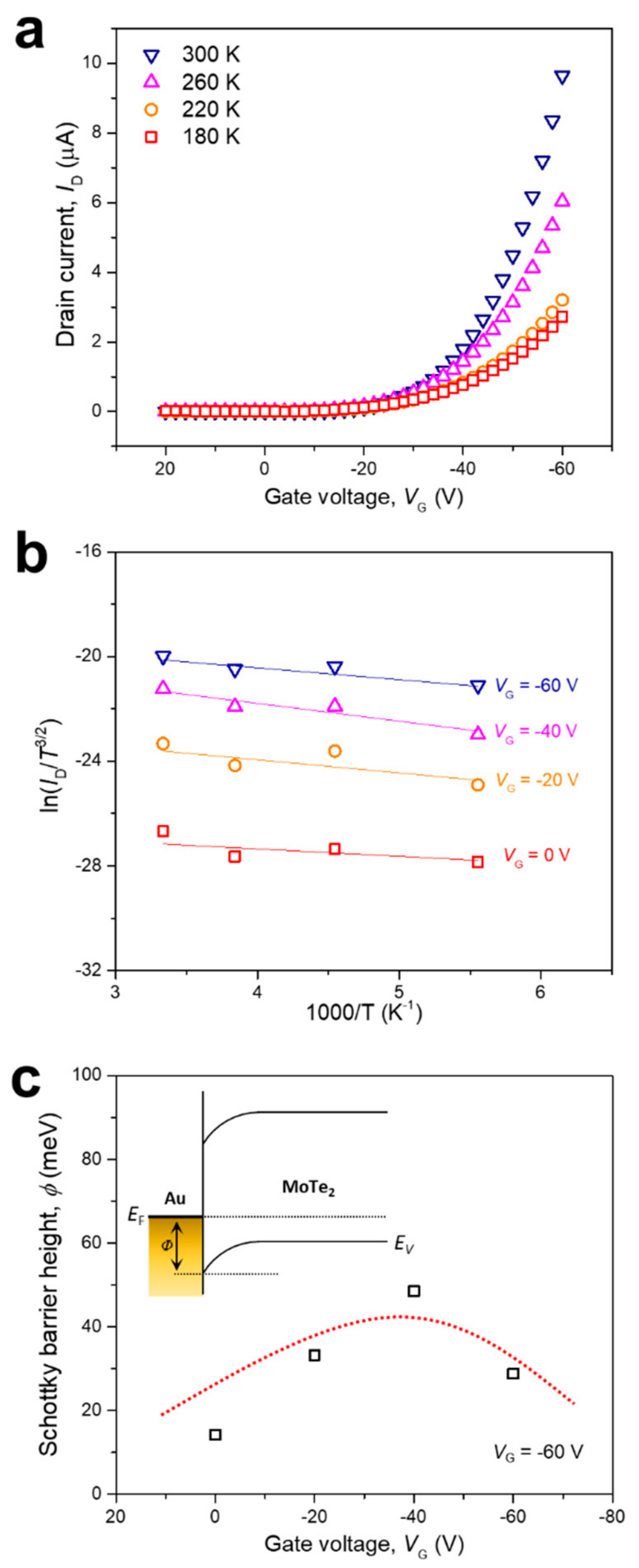
To further quantify the ohmic contact in these devices, the barrier height at the interface between the S/D electrodes and the MoTe2 channel was studied [36,47]. The electrical properties were characterized at various temperatures to measure the energy levels of the metallic and semiconducting layers in the 1T′-phase MoTe2 devices, as shown in Figure 4.
As the temperature increases, the drain current (ID) also increases due to the hopping transport, which dominates the charge transport in MoTe2 [48]. The increase in the current with temperature is due to the increased charge carriers at elevated temperatures, where the thermal energy is sufficient to overcome the activation energy. The results were fitted using the following thermal emission equation to obtain an Arrhenius plot of the laser-irradiated 1T′ MoTe2 devices at different gate voltages:
where IDS is current, A is the Richardson’s constant, T is the temperature, φB is the Schottky barrier, q is the charge constant, kB is the Boltzmann constant, VDS is the drain voltage, and n is the nonideal factor [32,49]. When VDS >> kBT, Equation (2) can be simplified as:
The Schottky energy barrier (φB) can be expressed as the slope of the simplified equation in a curve of ln(IDS/T3/2) versus 1000/T. The results were plotted at different VG values for the 1T′ MoTe2 FETs (Figure 4b). Finally, to obtain the nonideal factor (n), which is required to calculate φB for each slope, we used the following equation:
where Rs is the series resistance. We calculated n as the slope of a curve of dVDS/dIDS versus 1/IDS and obtained a value of 9.93 (Figure S2) [36,49]. The value of φB was calculated from these results (Figure 4c). When a zero-gate voltage was applied, the Schottky energy barrier was lower in the 1T′ MoTe2 device than in the 2H MoTe2 device, demonstrating that 1T′ MoTe2 forms a sharper interface between the electrode and the semiconducting layer than 2H MoTe2 (Figure S3). Note that the difference in transistor polarity between the 2H and 1T′ devices is explained simply by modifying the Schottky barrier height by laser irradiation. An advantage of the 1T′ device is that the S/D electrodes are side contacts rather than vertical contacts, providing better device properties [50,51]. Furthermore, this result is fundamentally different from previously reported results on chemical doping. The transistor polarity change mechanism preserves the electron and hole mobilities. It efficiently improves electron mobility with a facile approach. Moreover, 1T′-phase devices are highly independent of the metal of the S/D electrodes. We designed 1T′ MoTe2 devices with the same electrodes and achieved a yield of nearly 100% with consistent performance. Additionally, an ohmic-like contact was achieved at the interface between the active layer and electrodes, which improved the charge carrier injection without barriers. Although the 1T′ phase is metastable, it has been demonstrated that stability can be maintained under environmental conditions after facile laser irradiation.
4. Conclusions
In summary, we developed a facile method for phase tuning from 2H to 1T′ MoTe2 by laser irradiation. This method produces a 1T′ MoTe2 monolayer that facilitates charge injection at the interface and thus improves the electrical characteristics of the MoTe2 FETs. Moreover, we showed that phase tunability could help effectively reduce the contact resistance at the interface between the S/D electrodes and the MoTe2 channel, thus providing high carrier mobility of the FETs. Additionally, we demonstrated that the 1T′ phase of MoTe2 is a heterophase homojunction electrode with a low contact resistance value of 93 kΩ·μm at zero gate bias. The low contact resistance results in a high on-current of 3.1 mA1/2, and a high charge carrier mobility of 16.1 cm2 V−1s−1. Our work demonstrates that phase engineering is a practical approach for improving the performance of MoTe2 devices.
Supplementary Materials
The following are available online at https://www.mdpi.com/article/10.3390/nano11112805/s1, Figure S1: Optical image of the CVD-grown MoTe2 on the SiO2/Si substrate, Figure S2: I-V curve of MoTe2 FETs, Figure S3: Schottky barrier height of MoTe2 FETs. Table S1. Comparison the device performances.
Author Contributions
Conceptualization, J.K. (Junyoung Kim), and E.L.; methodology, G.Y.B.; software, E.L.; validation, G.Y.B., J.K. (Jinsung Kim), and S.L.; formal analysis, J.K. (Junyoung Kim); investigation, G.Y.B. and J.K. (Jinsung Kim); resources, J.K. (Junyoung Kim); data curation, J.K. (Junyoung Kim), and S.L.; writing—original draft preparation, J.K. (Junyoung Kim), and E.L.; writing—review and editing, J.K. (Junyoung Kim), and E.L.; visualization, E.L.; supervision, E.L.; project administration, E.L.; funding acquisition, E.L.; contributed equally, G.Y.B., J.K. (Jinsung Kim), and J.K. (Junyoung Kim) All authors have read and agreed to the published version of the manuscript.
Funding
This research was funded by National Research Foundation of Korea (NRF) grant funded by the Korean government (MSIT) (No. 2021R1G1A1093058).
Data Availability Statement
Not applicable.
Acknowledgments
The authors acknowledge the illustration support from Noah Studio LLC, Dallas, TX, USA.
Conflicts of Interest
The authors declare no conflict of interest.
References
- Radisavljevic, B.; Radenovic, A.; Brivio, J.; Giacometti, V.; Kis, A. Single-layer MoS2 transistors. Nat. Nanotechnol. 2011, 6, 147–150. [Google Scholar] [CrossRef]
- Zhang, Z.; Chen, P.; Duan, X.; Zang, K.; Luo, J.; Duan, X. Robust epitaxial growth of two-dimensional heterostructures, multiheterostructures, and superlattices. Science 2017, 357, 788–792. [Google Scholar] [CrossRef] [Green Version]
- Li, X.; Cai, W.; An, J.; Kim, S.; Nah, J.; Yang, D.; Piner, R.; Velamakanni, A.; Jung, I.; Tutuc, E.; et al. Large-Area Synthesis of High-Quality and Uniform Graphene Films on Copper Foils. Science 2009, 324, 1312–1314. [Google Scholar] [CrossRef] [Green Version]
- Pradhan, N.R.; Rhodes, D.; Feng, S.; Xin, Y.; Memaran, S.; Moon, B.-H.; Terrones, H.; Terrones, M.; Balicas, L. Field-Effect Transistors Based on Few-Layered α-MoTe2. ACS Nano 2014, 8, 5911–5920. [Google Scholar] [CrossRef] [PubMed] [Green Version]
- Shen, D.W.; Xie, B.P.; Zhao, J.F.; Yang, L.X.; Fang, L.; Shi, J.; He, R.H.; Lu, D.H.; Wen, H.H.; Feng, D.L. Novel Mechanism of a Charge Density Wave in a Transition Metal Dichalcogenide. Phys. Rev. Lett. 2007, 99, 216404. [Google Scholar] [CrossRef] [PubMed] [Green Version]
- Zhang, Y.J.; Oka, T.; Suzuki, R.; Ye, J.T.; Iwasa, Y. Electrically Switchable Chiral Light-Emitting Transistor. Science 2014, 344, 725–728. [Google Scholar] [CrossRef] [PubMed]
- Choi, W.; Kim, J.; Lee, E.; Mehta, G.; Prasad, V. Asymmetric 2D MoS2 for Scalable and High-Performance Piezoelectric Sensors. ACS Appl. Mater. Interfaces 2021, 13, 13596–13603. [Google Scholar] [CrossRef] [PubMed]
- Lee, E.; Kim, J.; An, T.K. Direct growth of CVD graphene on 3D-architectured substrates for highly stable tactile sensors. Chin. J. Phys. 2020, 67, 569–575. [Google Scholar] [CrossRef]
- Kim, J.; Lee, E.; Mehta, G.; Choi, W. Stable and high-performance piezoelectric sensor via CVD grown WS2. Nanotechnology 2020, 31, 445203. [Google Scholar] [CrossRef]
- Lee, E.; Kim, J.; Bhoyate, S.; Cho, K.; Choi, W. Realizing Scalable Two-Dimensional MoS2 Synaptic Devices for Neuromorphic Computing. Chem. Mater. 2020, 32, 10447–10455. [Google Scholar] [CrossRef]
- Bhoyate, S.D.; Mhin, S.; Jeon, J.-E.; Park, K.; Kim, J.; Choi, W. Stable and High-Energy-Density Zn-Ion Rechargeable Batteries Based on a MoS2-Coated Zn Anode. ACS Appl. Mater. Interfaces 2020, 12, 27249–27257. [Google Scholar] [CrossRef] [PubMed]
- Qian, X.; Liu, J.; Fu, L.; Li, J. Quantum spin Hall effect in two-dimensional transition metal dichalcogenides. Science 2014, 346, 1344–1347. [Google Scholar] [CrossRef] [Green Version]
- Chhowalla, M.; Shin, H.S.; Eda, G.; Li, L.-J.; Loh, K.; Zhang, H. The chemistry of two-dimensional layered transition metal dichalcogenide nanosheets. Nat. Chem. 2013, 5, 263–275. [Google Scholar] [CrossRef] [PubMed]
- Vellinga, M.; de Jonge, R.; Haas, C. Semiconductor to metal transition in MoTe2. J. Solid State Chem. 1970, 2, 299–302. [Google Scholar] [CrossRef]
- Ali, M.N.; Xiong, J.; Flynn, S.; Tao, J.; Gibson, Q.D.; Schoop, L.; Liang, T.; Haldolaarachchige, N.; Hirschberger, M.; Ong, N.P.; et al. Large, non-saturating magnetoresistance in WTe2. Nature 2014, 514, 205–208. [Google Scholar] [CrossRef] [PubMed] [Green Version]
- Zandt, T.; Dwelk, H.; Janowitz, C.; Manzke, R. Quadratic temperature dependence up to 50 K of the resistivity of metallic MoTe2. J. Alloy. Compd. 2007, 442, 216–218. [Google Scholar] [CrossRef]
- Morgado, J.; Alcacer, L.; Henriques, R.; Lopes, E.B.; Almeida, M.; Fourmigué, M. Preparation and characterization of CPP2I3-δ single crystals. Synth. Met. 1993, 56, 1735–1740. [Google Scholar] [CrossRef]
- Enyashin, A.N.; Yadgarov, L.; Houben, L.; Popov, I.; Weidenbach, M.; Tenne, R.; Bar Sadan, M.; Seifert, G. New Route for Stabilization of 1T-WS2 and MoS2 Phases. J. Phys. Chem. C 2011, 115, 24586–24591. [Google Scholar] [CrossRef] [Green Version]
- Lin, Y.-C.; Dumcenco, D.O.; Huang, Y.-S.; Suenaga, K. Atomic mechanism of the semiconducting-to-metallic phase transition in single-layered MoS2. Nat. Nanotechnol. 2014, 9, 391–396. [Google Scholar] [CrossRef]
- Pan, X.-C.; Chen, X.; Liu, H.; Feng, Y.; Wei, Z.; Zhou, Y.; Chi, Z.; Pi, L.; Yen, F.; Song, F.; et al. Pressure-driven dome-shaped superconductivity and electronic structural evolution in tungsten ditelluride. Nat. Commun. 2015, 6, 7805. [Google Scholar] [CrossRef] [Green Version]
- Kang, D.; Zhou, Y.; Yi, W.; Yang, C.; Guo, J.; Shi, Y.; Zhang, S.; Wang, Z.; Zhang, C.; Jiang, S.; et al. Superconductivity emerging from a suppressed large magnetoresistant state in tungsten ditelluride. Nat. Commun. 2015, 6, 7804. [Google Scholar] [CrossRef] [PubMed] [Green Version]
- Qi, Y.; Naumov, P.; Ali, M.N.; Rajamathi, C.R.; Schnelle, W.; Barkalov, O.; Hanfland, M.; Wu, S.-C.; Shekhar, C.; Sun, Y.; et al. Superconductivity in Weyl semimetal candidate MoTe2. Nat. Commun. 2016, 7, 11038. [Google Scholar] [CrossRef] [PubMed] [Green Version]
- Wang, Z.; Gresch, D.; Soluyanov, A.; Xie, W.; Kushwaha, S.; Dai, X.; Troyer, M.; Cava, R.J.; Bernevig, B.A. MoTe2: A Type-II Weyl Topological Metal. Phys. Rev. Lett. 2016, 117, 056805. [Google Scholar] [CrossRef] [PubMed] [Green Version]
- Soluyanov, A.; Gresch, D.; Wang, Z.; Wu, Q.; Troyer, M.; Dai, X.; Bernevig, B.A. Type-II Weyl semimetals. Nature 2015, 527, 495–498. [Google Scholar] [CrossRef] [PubMed] [Green Version]
- Wu, S.; Fatemi, V.; Gibson, Q.D.; Watanabe, K.; Taniguchi, T.; Cava, R.J.; Jarillo-Herrero, P. Observation of the quantum spin Hall effect up to 100 kelvin in a monolayer crystal. Science 2018, 359, 76–79. [Google Scholar] [CrossRef] [Green Version]
- Xu, X.; Chen, S.; Liu, S.; Cheng, X.; Xu, W.; Li, P.; Wan, Y.; Yang, S.; Gong, W.; Yuan, K.; et al. Millimeter-Scale Single-Crystalline Semiconducting MoTe2 via Solid-to-Solid Phase Transformation. J. Am. Chem. Soc. 2019, 141, 2128–2134. [Google Scholar] [CrossRef]
- Hou, W.; Azizimanesh, A.; Sewaket, A.; Peña, T.; Watson, C.; Liu, M.; Askari, H.; Wu, S.M. Strain-based room-temperature non-volatile MoTe2 ferroelectric phase change transistor. Nat. Nanotechnol. 2019, 14, 668–673. [Google Scholar] [CrossRef] [Green Version]
- Wang, Y.; Xiao, J.; Zhu, H.; Li, Y.; Alsaid, Y.; Fong, K.Y.; Zhou, Y.; Wang, S.; Shi, W.; Wang, Y.; et al. Structural phase transition in monolayer MoTe2 driven by electrostatic doping. Nature 2017, 550, 487–491. [Google Scholar] [CrossRef]
- Zhang, C.; Kc, S.; Nie, Y.; Liang, C.; Vandenberghe, W.G.; Longo, R.C.; Zheng, Y.; Kong, F.; Hong, S.; Wallace, R.M.; et al. Charge Mediated Reversible Metal–Insulator Transition in Monolayer MoTe2 and WxMo1–xTe2 Alloy. ACS Nano 2016, 10, 7370–7375. [Google Scholar] [CrossRef]
- Keum, D.H.; Cho, S.; Kim, J.H.; Choe, D.-H.; Sung, H.-J.; Kan, M.; Kang, H.; Hwang, J.-Y.; Kim, S.W.; Yang, H.; et al. Bandgap opening in few-layered monoclinic MoTe2. Nat. Phys. 2015, 11, 482–486. [Google Scholar] [CrossRef]
- Das, S.; Chen, H.-Y.; Penumatcha, A.V.; Appenzeller, J. High Performance Multilayer MoS2 Transistors with Scandium Contacts. Nano Lett. 2012, 13, 100–105. [Google Scholar] [CrossRef]
- Chen, J.-R.; Odenthal, P.M.; Swartz, A.G.; Floyd, G.C.; Wen, H.; Luo, K.Y.; Kawakami, R.K. Control of Schottky Barriers in Single Layer MoS2 Transistors with Ferromagnetic Contacts. Nano Lett. 2013, 13, 3106–3110. [Google Scholar] [CrossRef]
- Popov, I.Y.; Seifert, G.; Tománek, D. Designing Electrical Contacts to MoS2 Monolayers: A Computational Study. Phys. Rev. Lett. 2012, 108, 156802. [Google Scholar] [CrossRef] [Green Version]
- Buscema, M.; Barkelid, M.; Zwiller, V.; Van Der Zant, H.S.J.; Steele, G.A.; Castellanos-Gomez, A. Large and Tunable Photothermoelectric Effect in Single-Layer MoS2. Nano Lett. 2013, 13, 358–363. [Google Scholar] [CrossRef] [PubMed] [Green Version]
- Ghatak, S.; Pal, A.N.; Ghosh, A. Nature of Electronic States in Atomically Thin MoS2 Field-Effect Transistors. ACS Nano 2011, 5, 7707–7712. [Google Scholar] [CrossRef] [PubMed] [Green Version]
- Lee, E.; Lee, S.G.; Lee, W.H.; Lee, H.C.; Nguyen, N.N.; Yoo, M.S.; Cho, K. Direct CVD Growth of a Graphene/MoS2 Heterostructure with Interfacial Bonding for Two-Dimensional Electronics. Chem. Mater. 2020, 32, 4544–4552. [Google Scholar] [CrossRef]
- Fang, H.; Tosun, M.; Seol, G.; Chang, T.C.; Takei, K.; Guo, J.; Javey, A. Degenerate n-Doping of Few-Layer Transition Metal Dichalcogenides by Potassium. Nano Lett. 2013, 13, 1991–1995. [Google Scholar] [CrossRef] [PubMed]
- Mak, K.F.; Shan, K.F.M.J. Photonics and optoelectronics of 2D semiconductor transition metal dichalcogenides. Nat. Photon. 2016, 10, 216–226. [Google Scholar] [CrossRef]
- Yamamoto, M.; Wang, S.T.; Ni, M.; Lin, Y.-F.; Li, S.-L.; Aikawa, S.; Jian, W.-B.; Ueno, K.; Wakabayashi, K.; Tsukagoshi, K. Strong Enhancement of Raman Scattering from a Bulk-Inactive Vibrational Mode in Few-Layer MoTe2. ACS Nano 2014, 8, 3895–3903. [Google Scholar] [CrossRef]
- Goldstein, T.; Chen, S.-Y.; Tong, J.; Xiao, D.; Ramasubramaniam, A.; Yan, J. Raman scattering and anomalous Stokes–anti-Stokes ratio in MoTe2 atomic layers. Sci. Rep. 2016, 6, 28024. [Google Scholar] [CrossRef] [PubMed]
- Cho, H.; Kim, S.; Kim, S.; Zhao, J.H.; Seok, J.; Keum, J.; Baik, D.H.; Choe, J.; Chang, D.H.; Suenaga, K.J.; et al. Phase patterning for ohmic homojunction contact in MoTe2. Science 2015, 349, 625–628. [Google Scholar] [CrossRef]
- Zhou, L.; Xu, K.; Zubair, A.; Liao, A.D.; Fang, W.; Ouyang, F.; Lee, Y.-H.; Ueno, K.; Saito, R.; Palacios, T.; et al. Large-Area Synthesis of High-Quality Uniform Few-Layer MoTe2. J. Am. Chem. Soc. 2015, 137, 11892–11895. [Google Scholar] [CrossRef]
- Naylor, C.H.; Parkin, W.M.; Ping, J.; Gao, Z.; Zhou, Y.R.; Kim, Y.; Streller, F.; Carpick, R.W.; Rappe, A.M.; Drndić, M.; et al. Monolayer Single-Crystal 1T′-MoTe2 Grown by Chemical Vapor Deposition Exhibits Weak Antilocalization Effect. Nano Lett. 2016, 16, 4297–4304. [Google Scholar] [CrossRef] [Green Version]
- Li, H.; Tsai, C.; Koh, A.L.; Cai, L.; Contryman, A.W.; Fragapane, A.H.; Zhao, J.; Han, H.S.; Manoharan, H.C.; Abild-Pedersen, F.; et al. Activating and optimizing MoS2 basal planes for hydrogen evolution through the formation of strained sulphur vacancies. Nat. Mater. 2016, 15, 364. [Google Scholar] [CrossRef] [PubMed]
- Somvanshi, D.; Kallatt, S.; Venkatesh, C.; Nair, S.; Gupta, G.; Anthony, J.K.; Karmakar, D.; Majumdar, K. Nature of carrier injection in metal/2D-semiconductor interface and its implications for the limits of contact resistance. Phys. Rev. B 2017, 96, 205423–205433. [Google Scholar] [CrossRef] [Green Version]
- Lu, Q.; Liu, Y.; Han, G.; Fang, C.; Shao, Y.; Zhang, J.; Hao, Y. Experimental investigation of the contact resistance of Graphene/MoS2 interface treated with O2 plasma. Superlattices Microstruct. 2018, 114, 421–427. [Google Scholar] [CrossRef]
- Kappera, R.; Voiry, D.; Yalcin, S.E.; Branch, B.; Gupta, G.; Mohite, A.; Chhowalla, M. Phase-engineered low-resistance contacts for ultrathin MoS2 transistors. Nat. Mater. 2014, 13, 1128–1134. [Google Scholar] [CrossRef] [PubMed]
- Park, J.H.; Jung, E.H.; Jung, J.W.; Jo, W.H. A Fluorinated Phenylene Unit as a Building Block for High-Performance n-Type Semiconducting Polymer. Adv. Mater. 2013, 25, 2583–2588. [Google Scholar] [CrossRef]
- Yu, L.; Lee, Y.-H.; Ling, X.; Santos, E.J.G.; Shin, Y.C.; Lin, Y.; Dubey, M.; Kaxiras, E.; Kong, J.; Wang, H.; et al. Graphene/MoS2 Hybrid Technology for Large-Scale Two-Dimensional Electronics. Nano Lett. 2014, 14, 3055–3063. [Google Scholar] [CrossRef] [PubMed] [Green Version]
- Das, S.; Appenzeller, J. Where Does the Current Flow in Two-Dimensional Layered Systems. Nano Lett. 2013, 13, 3396–3402. [Google Scholar] [CrossRef]
- Kim, S.; Konar, A.; Hwang, W.-S.; Lee, J.H.; Lee, J.; Yang, J.; Jung, C.; Kim, H.; Yoo, J.-B.; Choi, J.-Y.; et al. High-mobility and low-power thin-film transistors based on multilayer MoS2 crystals. Nat. Commun. 2012, 3, 1011. [Google Scholar] [CrossRef] [PubMed] [Green Version]
Figure 1.
Characterization of CVD-grown MoTe2: (a) Schematic of CVD synthesis of MoTe2 on SiO2/Si substrate using salt-assisted growth; (b) Optical microscopy image of triangular monolayered MoTe2 nuclei on the SiO2/Si substrate. The scale bar is 2 μm; (c) AFM image of MoTe2 and the height profile corresponding to the white dashed line; the thickness of the MoTe2 is 0.87 nm; (d) Raman spectra of MoTe2 at various laser irradiation times. The inset shows the evolution of the Ag peak related to the 1T′ phase of MoTe2 with time. XPS spectra show (e) Mo 3d and (f) Te 3d peaks of the 1T′ and 2H phases of MoTe2.
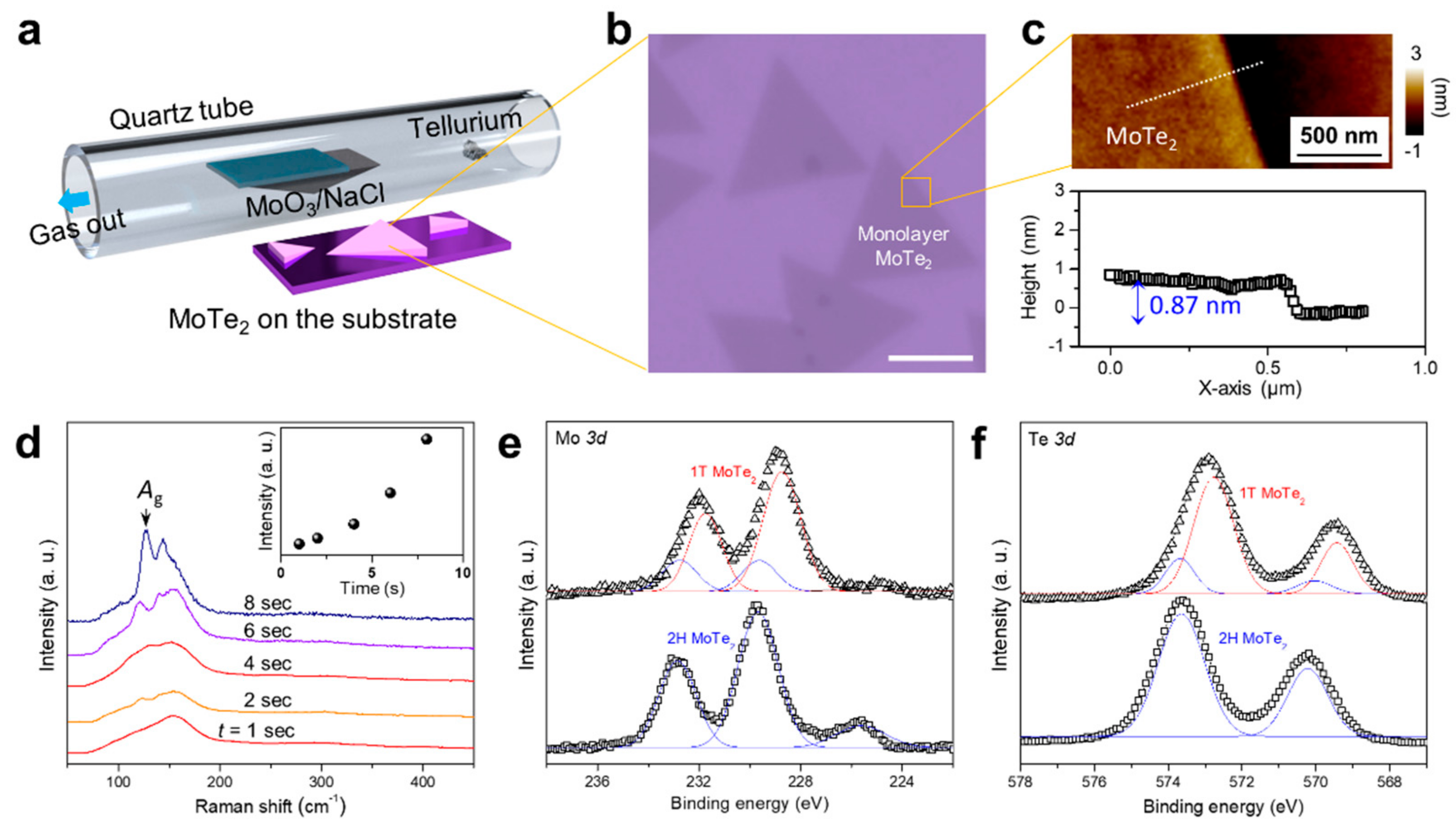
Figure 2.
Electrical characterization of 2H and 1T′-phase of MoTe2 FETs: (a) Schematic structure of MoTe2 FETs on SiO2/Si substrate; the dimensions of the MoTe2 FETs are the following: channel length 20 µm and width 400 µm. (b) Two-dimensional Ag Raman mapping image of MoTe2 FETs on SiO2/Si substrate after laser irradiation. Transfer curves of (c) 2H MoTe2 and (d) 1T′ MoTe2 FETs after laser irradiation; (e) Statistical diagram of the measured carrier mobilities; (f) On/off ratio of the 36 fabricated 2H and 1T′ FETs.
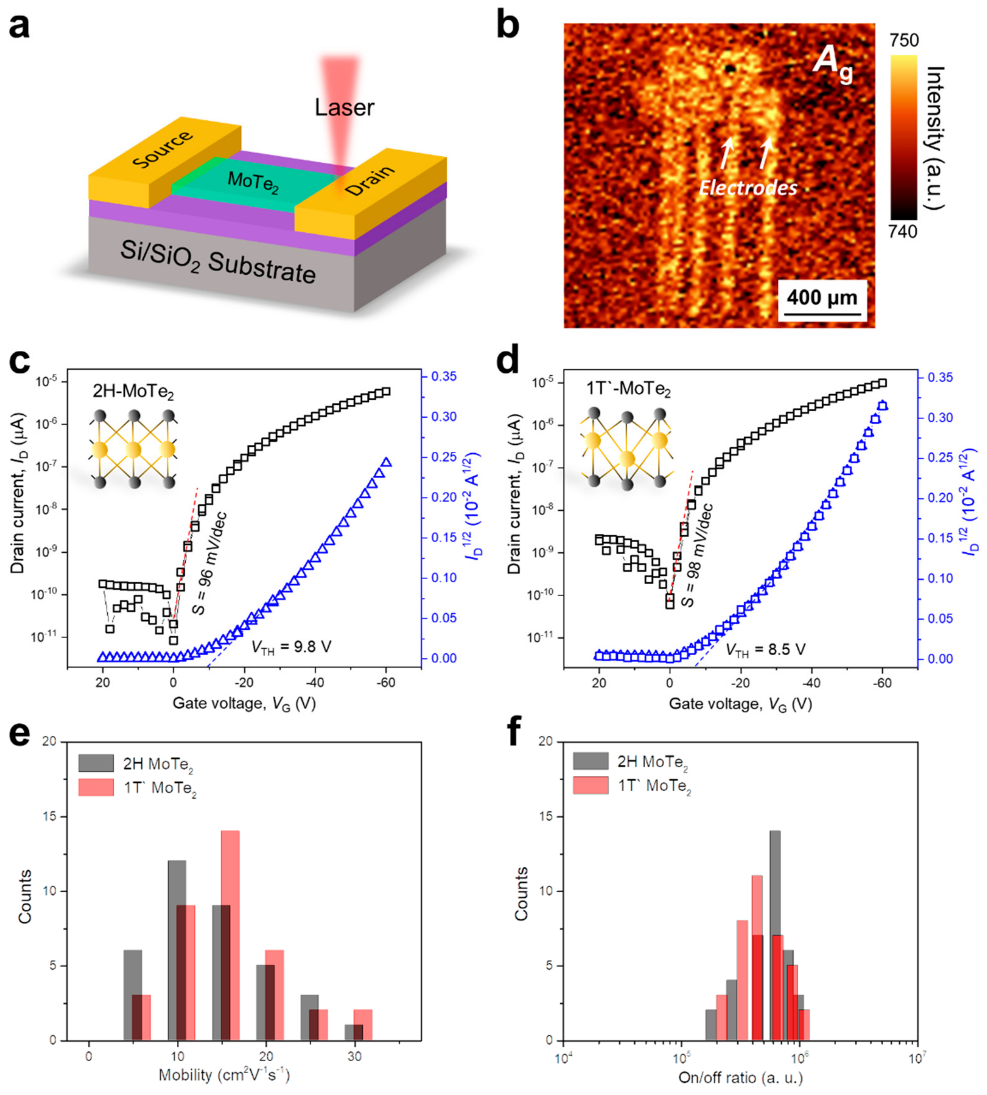
Figure 3.
Contact resistance of the 2H-phase and 1T′-phase of MoTe2 FETs: (a) 2H MoTe2 and (b) 1T′ MoTe2 FETs after laser irradiation. The channel width is normalized using the resistance obtained from 2H MoTe2 FETs; Output curves of (c) 2H and (d) 1T′-phase MoTe2 FETs after laser irradiation; the FETs have gate voltages ranging from 0 to −60 V.
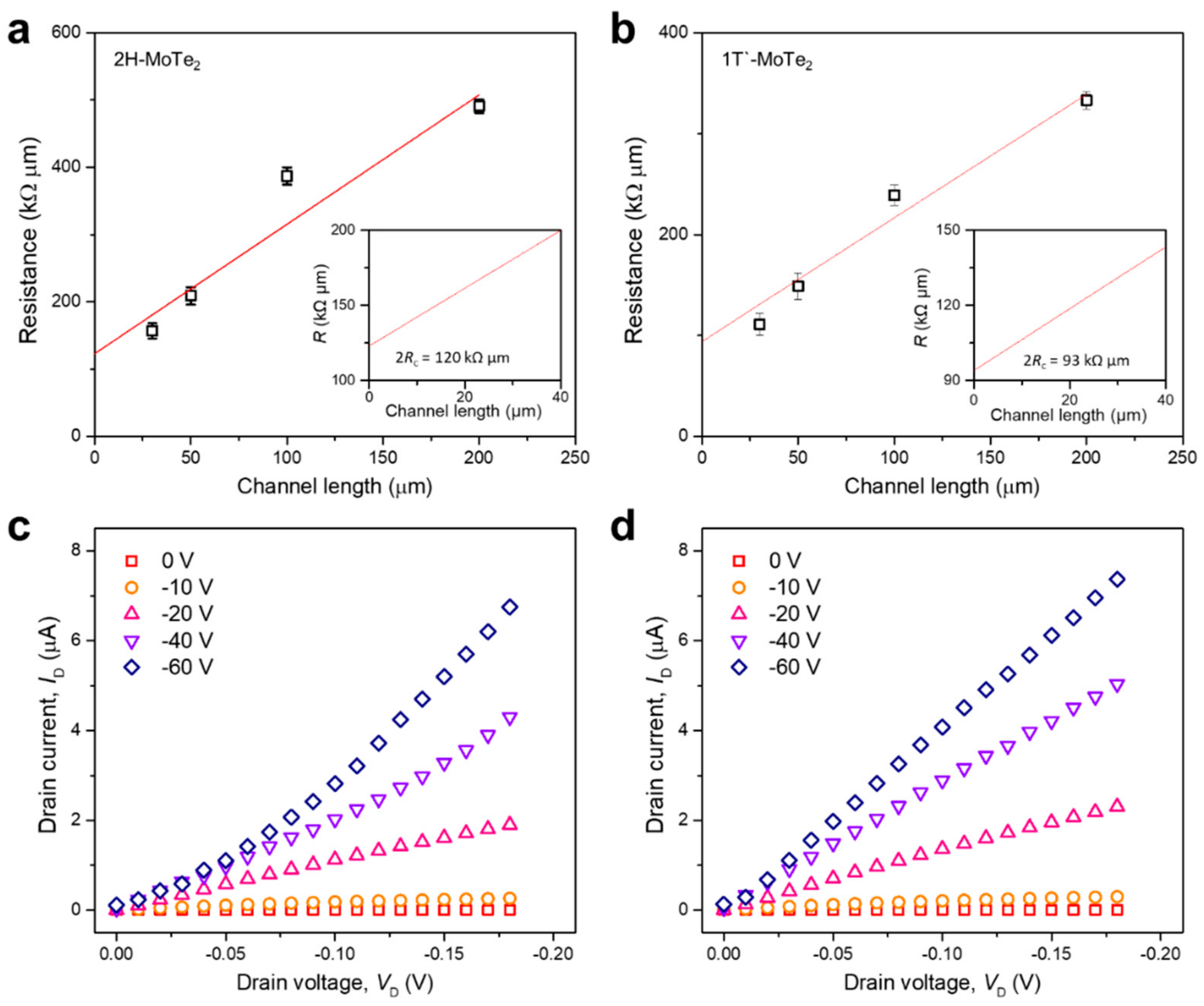
Figure 4.
Transfer curves and Schottky barrier of 1T′ MoTe2 FETs at various temperatures: (a) Transfer curves obtained from laser-irradiated 1T′ MoTe2 FETs at temperatures ranging from 180 to 300 K; (b) Arrhenius plot of laser-irradiated 1T′ MoTe2 FETs with gate voltages ranging from 0 V to −60 V; (c) Schottky barrier height of laser-irradiated 1T′ MoTe2 FETs. The inset shows the schematic of the Schottky barrier of p-type MoTe2 with contact to the Au electrode.
Publisher’s Note: MDPI stays neutral with regard to jurisdictional claims in published maps and institutional affiliations. |
© 2021 by the authors. Licensee MDPI, Basel, Switzerland. This article is an open access article distributed under the terms and conditions of the Creative Commons Attribution (CC BY) license (https://creativecommons.org/licenses/by/4.0/).
Share and Cite
MDPI and ACS Style
Bae, G.Y.; Kim, J.; Kim, J.; Lee, S.; Lee, E. MoTe2 Field-Effect Transistors with Low Contact Resistance through Phase Tuning by Laser Irradiation. Nanomaterials 2021, 11, 2805. https://doi.org/10.3390/nano11112805
AMA Style
Bae GY, Kim J, Kim J, Lee S, Lee E. MoTe2 Field-Effect Transistors with Low Contact Resistance through Phase Tuning by Laser Irradiation. Nanomaterials. 2021; 11(11):2805. https://doi.org/10.3390/nano11112805
Chicago/Turabian StyleBae, Geun Yeol, Jinsung Kim, Junyoung Kim, Siyoung Lee, and Eunho Lee. 2021. "MoTe2 Field-Effect Transistors with Low Contact Resistance through Phase Tuning by Laser Irradiation" Nanomaterials 11, no. 11: 2805. https://doi.org/10.3390/nano11112805
Note that from the first issue of 2016, this journal uses article numbers instead of page numbers. See further details here.