Article

Electric Transport in Few-Layer ReSe2 Transistors Modulated by Air Pressure and Light

1
Department of Physics “E.R. Caianiello”, University of Salerno, 84084 Fisciano, SA, Italy
2
CNR-SPIN, 84084 Fisciano, SA, Italy
3
University of Exeter, Stocker Road 6, Exeter EX4 4QL, Devon, UK
*
Author to whom correspondence should be addressed.
Nanomaterials 2022, 12(11), 1886; https://doi.org/10.3390/nano12111886
Submission received: 29 April 2022 / Revised: 19 May 2022 / Accepted: 27 May 2022 / Published: 31 May 2022
(This article belongs to the Special Issue Electronic Nanodevices)

Abstract

:
We report the fabrication and optoelectronic characterization of field-effect transistors (FETs) based on few-layer ReSe2. The devices show n-type conduction due to the Cr contacts that form low Schottky barriers with the ReSe2 nanosheet. We show that the optoelectronic performance of these FETs is strongly affected by air pressure, and it undergoes a dramatic increase in conductivity when the pressure is lowered below the atmospheric one. Surface-adsorbed oxygen and water molecules are very effective in doping ReSe2; hence, FETs based on this two-dimensional (2D) semiconductor can be used as an effective air pressure gauge. Finally, we report negative photoconductivity in the ReSe2 channel that we attribute to a back-gate-dependent trapping of the photo-excited charges.

1. Introduction

Rhenium diselenide (ReSe2) is a member of the layered transition metal dichalcogenides (TMDs), which has attracted a lot of attention due to the extremely anisotropic electrical, optical and mechanical properties stemming from the strong in-plane anisotropy consequence of its reduced crystal symmetry [1,2,3,4]. Contrary to other hexagonal TMDs, the room temperature thermodynamically stable 1T phase for ReSe2 has a distorted triclinic symmetry, which endows the material with anisotropic responses in many properties [5,6,7].
Monolayer ReSe2 has an indirect bandgap of 1.34 eV [8,9,10], reducing to 0.98 eV [6] for bulk ReSe2, with a weak layer dependency. In general, an increase in the layer thickness causes a reduction in band-gap energy and the loss of electric properties of thick ReSe2 [11].
ReSe2 has been employed in various electronic and optoelectronic functional devices in order to study its electrical and optical properties. Yang et al. reported that the mobility of ReSe2 nanosheets increases when the number of layers decreases and highlighted that the properties of ReSe2 can be tuned by the number of layers and gas molecule gating, making ReSe2 a promising material for future functional device applications [11]. Optically biaxial and highly anisotropic Mo-doped ReSe2 (Mo:ReSe2) was used to investigate the effects of physisorption of gas molecules on few-layer nanosheet-based photodetectors, reporting different sensitivity to the surrounding environment, prompt photoswitching, and high photoresponsivity [12].
The anisotropic nature of ReSe2 was revealed by Raman spectroscopy under linearly polarized excitations in a study by Zhang et al., who fabricated top-gate ReSe2 field-effect transistors (FETs), with a high on/off current ratio and a well-developed current saturation in the current–voltage characteristics at room temperature [7]. They synthesized ReSe2 directly onto hexagonal boron nitride (h-BN) substrates to improve the electron and hole mobility and demonstrated that the ReSe2-based photodetectors exhibit polarization-sensitive photoresponsivity due to the intrinsic linear dichroism, originating from high in-plane optical anisotropy, thus, identifying ReSe2 as a highly anisotropic two-dimensional (2D) material for novel electronic and optoelectronic applications.
Similarly, a near-infrared ReSe2 photodetector featuring high photoresponsivity and a short photoresponse time, in the order of 10 ms, was demonstrated by Kim and coworkers, achieving high photo and temporal responses simultaneously by applying a p-doping technique based on hydrochloric acid to a selected ReSe2 region [13].
Ambipolar FETs were obtained from multi-layer ReSe2, mechanically exfoliated onto a SiO2 layer by Pradhan et al., who demonstrated that it is possible to utilize the ambipolarity to fabricate logical elements or digital synthesizers [10]. Similarly, ambipolar all-2D ReSe2 FET with a h-BN gate dielectric and graphene contacts were investigated by Lee and coworkers, who used the ambipolar transfer characteristics, attributed to the tunable Fermi level of the graphene contact, to demonstrate an inverter in a logic circuit [14].
Corbet et al. proposed a method to improve the contact resistance in few-layer ReSe2 FETs, by up to three orders of magnitude, using ultra-high-vacuum annealing [15]. A low contact resistance was also obtained in single-layer ReSe2, encapsulated in h-BN using scandium/gold contacts, and this enabled Khan and coworkers [16] to measure a large field-effect charge carrier mobility and responsivity.
Xing et al. addressed the challenge of the controlled synthesis of high-quality ultrathin ReSe2, developing an approach for synthesizing 2D ReSe2 flakes with a thickness down to monolayer by chemical vapor transport, through carefully tuning the growth kinetics [17]. The FETs fabricated with such flakes showed n-type semiconducting behavior with mobility of a few cm2 V−1 s−1, comparable to the values measured using mechanically exfoliated flakes.
Polarization-resolved ReSe2 photodetectors were recently studied by Tian and Liu, who reported a van der Waals heterojunction ReSe2/WSe2-based photodetector, with high responsivity and detectivity at room temperature. Remarkably, they demonstrated that the photoresponse of their devices is a function of the polarized angle of the incident light, indicating the effective polarized light detection [18].
Pressure is commonly used to understand the interlayer interaction in layered materials. High-hydrostatic pressures of several kbar were applied to ReSe2 (and ReS2) exfoliated flakes and the effect on their optical properties was investigated, finding that the energies of the two main excitonic transitions decrease in energy with increasing pressure [19]. The negative pressure coefficients were attributed to the destabilization of the pz orbital with increasing pressure, demonstrating that ReSe2 does not exhibit a strong electronic decoupling and, hence, the optoelectronic properties of few-layered ReSe2 could be drastically different from the bulk form.
Conversely, the effect of low pressure on ReSe2 has been rarely investigated in the literature.
In the present study, we fabricate back-gate FETs with a few-layer ReSe2 channel and study the electric transport from room pressure down to 10−5 mbar. We find that air pressure has a dramatic effect on the channel conductivity, which increases by more than two orders of magnitude when the pressure decreases. We explain such behavior in terms of the desorption of oxygen and water molecules from the ReSe2 surface in high vacuum. Importantly, we observe that the effect of air pressure is reversible, highlighting that back-gate ReSe2 FETs can be exploited as effective pressure gauges. Moreover, we report a reduction of the channel conductivity when the device is illuminated, i.e., a negative photoconducticity, that has not been reported before for ReSe2. The dependence of the negative photoconductivity on the gate voltage suggests that photo-excited free charge carriers are attracted towards the gate and captured at the interface, with the dielectric layer contributing to the observed loss of conductivity.

2. Materials and Methods

Ultrathin ReSe2 flakes were exfoliated from bulk ReSe2 single crystals using a standard mechanical exfoliation method by adhesive tape. The flakes were transferred onto highly doped n-type (resistivity 0.005 Ω cm) silicon substrates, covered by 290 nm thick SiO2, which serves as a global back gate. Photolithography and standard lift-off process of evaporated Cr/Au (5 nm/100 nm) were applied to define metal contacts. Figure 1a reports the crystal structure and Figure 1b shows the schematic of a ReSe2 FET with the circuit used to control the Si/SiO2 back-gate and the source-drain bias on the 2D semiconducting channel. We adopted an interdigitated layout with 4 parallel channels corresponding to a total channel width W = 26.0 μ m and length L = 0.78 μ m . An optical top view of a typical device is shown in Figure 1c. The thickness of the flake was measured by an atomic force microscope (Nanosurf AG, Liestal, Switzerland), obtaining the height profile displayed in Figure 1d that confirms a thickness of 1.84 nm, corresponding to 3 layers [20].
Electric measurements were carried out in two-probe configuration in a Janis ST-500 Probe Station (Lake Shore Cryotronics, Inc., Westerville, OH, USA) equipped with nanoprobes connected to the source/drain leads (Figure 1b). The back-gate voltage was applied through the sample holder of the probe station which was in direct electrical contact to the Ag-pasted n-Si substrate. The measurements were performed by the source-measurement units of a semiconductor characterization system Keithley 4200 SCS (Tektronix, Inc., Beaverton, OR, USA), with current and voltage sensitivity better than 1 pA and 2 μV, respectively. For the transistor characterization, the source was grounded while the drain ( V ds ) and gate ( V gs ) voltages were either swept or stepped while the drain ( I d ) and gate ( I g ) currents were monitored. The measured gate leakage current was always < 10 pA, confirming the integrity of the SiO2 gate dielectric.
The electric measurements were performed at controlled air pressure, from room pressure to 10−5 mbar. Under the combined action of a rotatory and a turbomolecular pump connected in series to a probe station and a valve system, it was possible to control the pressure stepwise. The pressure was monitored through the pressure gauge TPG261 (Pfeiffer, Asslar, Deutschland). The photoresponse of the device was investigated using an array of 144 white LEDs with a spectrum ranging from 400 to 750 nm and peaks at 450 nm and 540 nm, a color temperature of 6000 K, and with 1 mW/cm2 intensity.

3. Results and Discussion

Initially, the ReSe2 transistor was characterized in dark and at room temperature and pressure, followed by investigating the effect of the lowering pressure in the same conditions of temperature and darkness. Finally, we explored the photoresponse of the fabricated device.

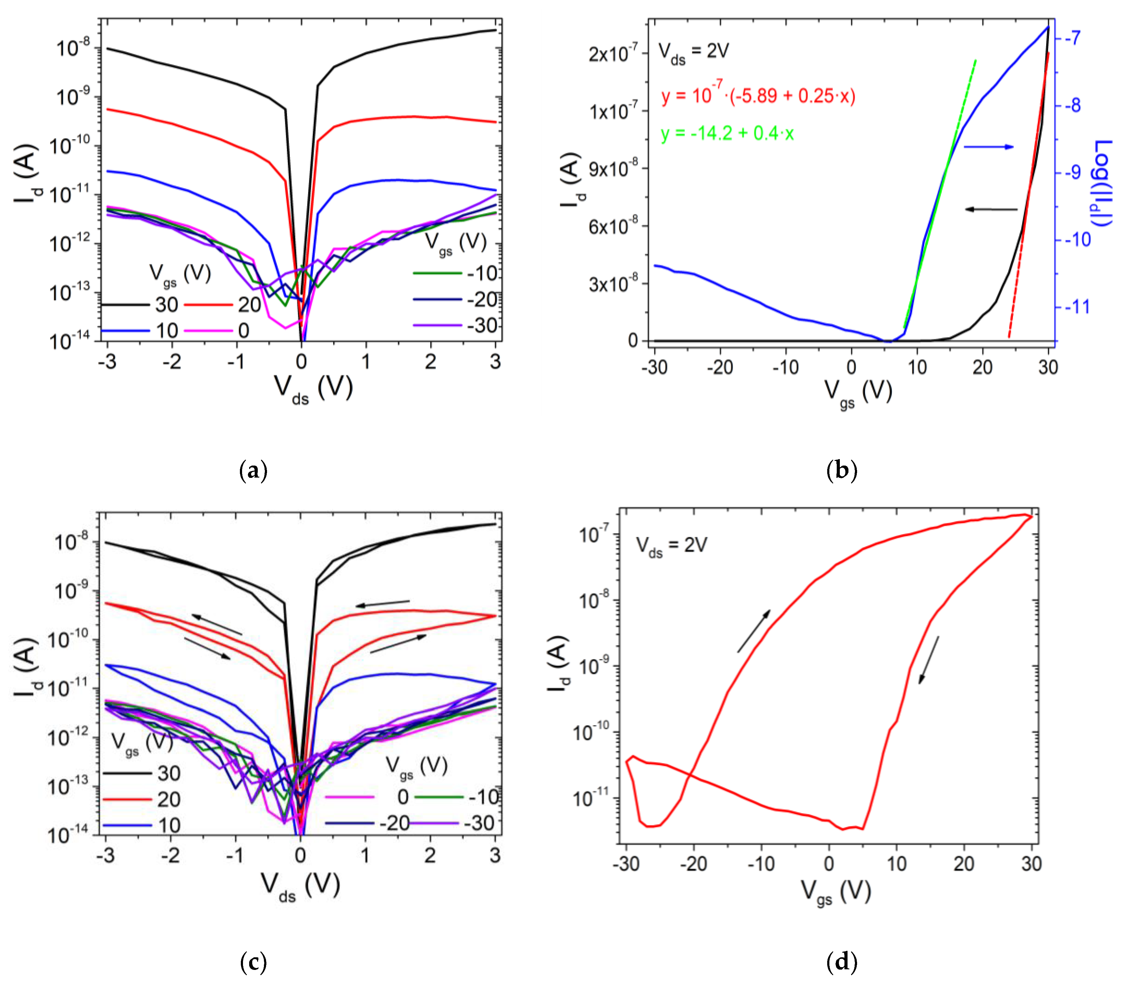
3.1. Transistor Characterization

Figure 2a,b report the output ( I d V ds at fixed V gs ) and transfer ( I d V gs at fixed V ds ) characteristics of the fabricated ReSe2 FET, respectively. We limited the drain bias to 3 V and gate voltage range to ± 30 V to prevent damage to the device and, in particular, to the SiO2 gate dielectric. The I d V ds curves (Figure 2a) show that the drain current is modulated by the gate voltage V gs and stays below 10 pA for negative V gs but increases abruptly for positive V gs . This behavior is typical of a n-type transistor [21,22]. Furthermore, for all gate voltages, the I d V ds curves are asymmetric, with slightly higher current at positive V ds , pointing to the formation of low Schottky barriers at the ReSe2/Cr/Au contacts [23,24,25,26]. The presence of a Schottky barrier is confirmed also by the limited current that reaches the maximum of 20 nA at V ds = 3   V .
The I d V gs transfer curves of Figure 2b, shown on both the linear and logarithmic scale, confirm the n-type behavior of the transistor, with off-state at V gs < 20   V and on-state for V gs > 20   V . The curve on the logarithmic scale shows an on/off current ratio higher than two orders of magnitude and a modest subthreshold swing SS 2.8 V/decade, typical of back-gate 2D transistors with limited gate efficiency and high interface defect density [27,28,29,30]. The smooth rise of I d at negative V gs indicates the appearance of a hole-type conduction. The carrier type can be controlled via the metal contacts. Dominant n-type behavior is obtained in ReSe2 transistors with low-work-function metal contacts, such as Al or Ti, whose Fermi level aligns above the conduction band minimum of ReSe2 [7,14,31]. As the conduction band minimum of ReSe2 is around of 4.5 eV and the valence band maximum is around 5.6 eV [31], the Fermi levels of Cr and Au that have work functions of 4.5 and 5.1 eV, respectively, align within the ReSe2 bandgap and can favor ambipolar conduction.
The transfer curve on the linear scale is used to estimate the field-effect mobility, μ FE , in the on-state of the transistor for V gs > 20   V . The mobility, evaluated as μ FE = L W 1 C ox V ds dI ds dV gs (here C ox = 1.15 × 10 8   F   cm 2 is the gate dielectric capacitance per unit area), results μ FE 0.03   cm 2   V 1   s 1 slightly lower than the μ FE     0.1 10   cm 2   V 1   s 1 , typically measured in few-layer ReSe2 FETs [5,7,10,11]. We also note that an increase in layer thickness causes a loss of electric properties in ReSe2 and, in particular, that few-layer ReSe2 exhibits lower mobility of two orders of magnitude or more than single-layer ReSe2 [11]. Furthermore, the presence of a Schottky barrier at the contacts [32,33], as well as intrinsic defects in the material and impurities located at the interface with the SiO2 layer or adsorbates on top of the channel from air exposure during the fabrication and the measurement process [10,34,35], acting as scattering or trapping centers, can contribute to decrease the mobility.
The x-axis intercept of the straight line that fits the transfer curve on the linear scale in Figure 2b is assumed as the threshold voltage V th of the transistor and is about 20 V, indicating a n-type enhancement mode device.
More insights in the electric transport through the ReSe2 channel can be gained from Figure 2c,d, which display a hysteresis on both the output and transfer curves when V ds or V gs are swept in a loop (the forward and reverse sweeps yield different curves). The presence of large hysteresis in the I d V ds characteristics has been reported before in monolayer MoS2 devices, where it was attributed to the multigrain structure of the material and exploited to enable resistive switching devices. The presence of grain boundaries provides the opportunity to fabricate memristors, owing to the phenomenon of migration of defects, such as sulphur vacancies at grain boundaries, by applying a high electric field [36]. The hysteretic behavior in Figure 2c points to a defective ReSe2 channel, possibly with Se vacancies, consistent with the n-type intrinsic doping and the low mobility. The presence of intrinsic and interfacial defects is confirmed by the huge hysteresis observed in the transfer curve in Figure 2d. Hysteresis in the transfer characteristic is very common in 2D-material-based transistors and has been widely studied and attributed to charge trapping inside the channel material, interface trap states or surface adsorbates [37,38]. The interaction with the SiO2 dielectric, i.e., the ReSe2/SiO2 interface, is of paramount importance. Indeed, the substitution of the SiO2 layer by a high-quality h-BN-insulating substrate, which is atomically flat and free of charge trapping sites, has been shown to result in a strong mitigation of the hysteresis [39].

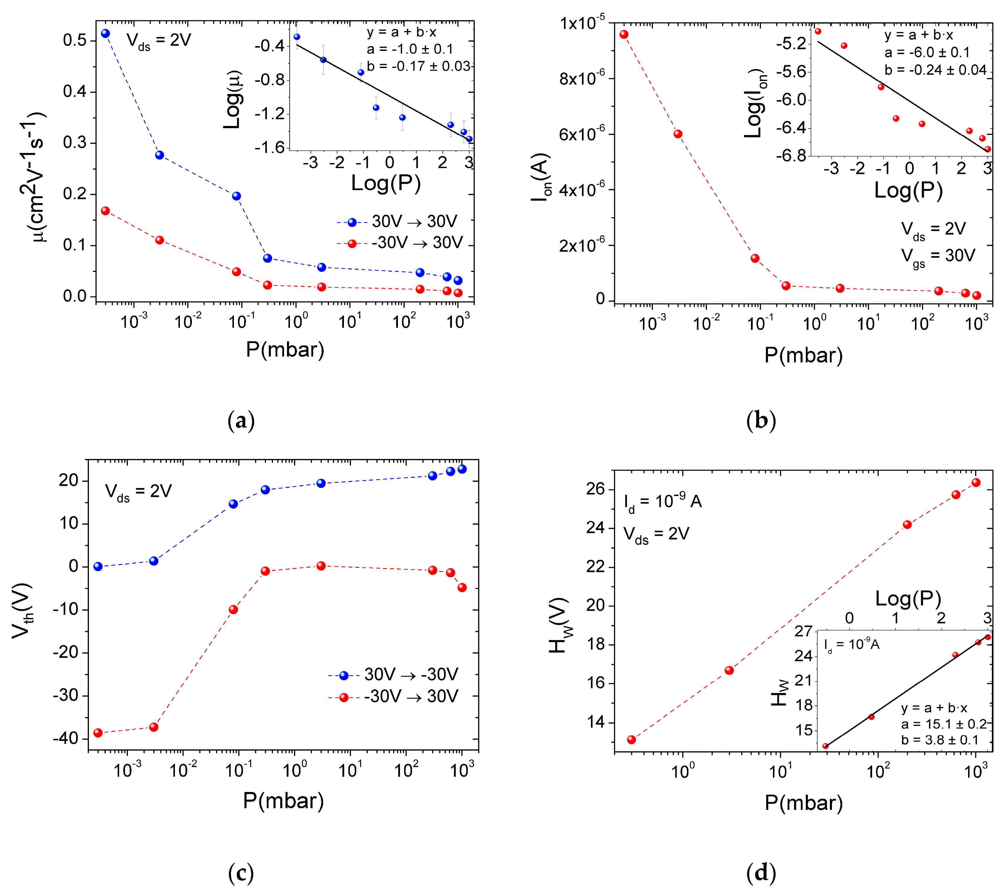
3.2. Pressure Behavior
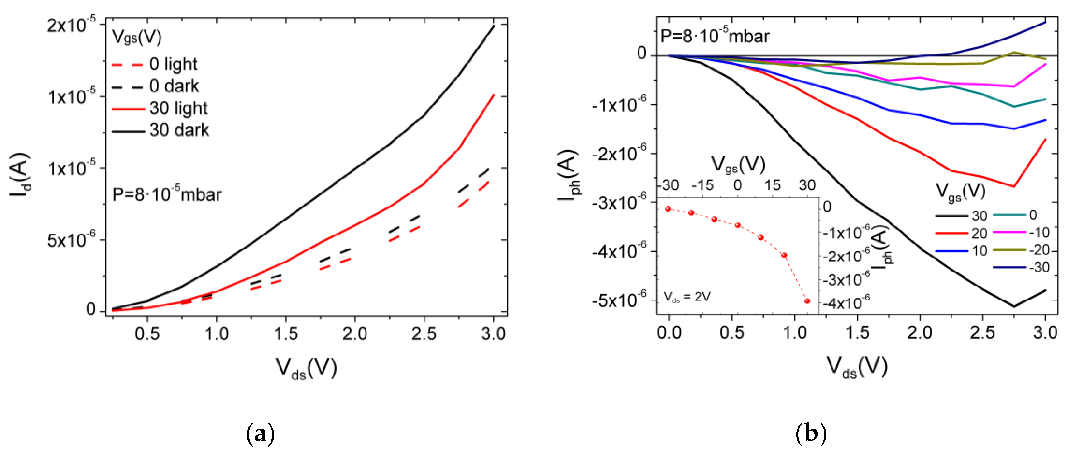
To investigate the effect of air pressure on the ReSe2 channel conductivity, we performed an electric transport measurement, lowering the atmospheric pressure down to 10−5 mbar. The measurements were performed after keeping the device at the given pressure for several hours to achieve a steady state. Figure 3a shows the output characteristics at three different pressures (room pressure, 3 mbar and 8 × 10 5 mbar) for increasing gate voltages, ranging from 0 V to 30 V, with steps of 10 V. It can be observed that the channel current increases at lower pressure while the hysteresis decreases, and the asymmetric behavior is unchanged. The reduced hysteresis indicates that surface adsorbates play an important role.
The same trend with increased current and reduced hysteresis at low pressure is displayed also by the transfer characteristics in Figure 3b. The low pressure, in particular, causes a dramatic change in the transfer characteristics with the transistor that does not turn off over the applied V gs range. The lowering pressure causes a left shift in the transfer characteristics, corresponding to a reduction in the threshold voltage V th , pointing to an increased n-type doping density. Such behavior can be explained as desorption of adsorbates from the ReSe2 surface. Adsorbed oxygen and water molecules, being electronegative, subtract electrons to the channel, thus, decreasing the conductivity (otherwise stated, oxygen and water counter-dope the n-type channel with holes). Their desorption has the two-fold beneficial effect of increasing the n-type doping and the mobility (see following), resulting in increased conductivity.
Figure 3c,d, which display the transfer characteristics for lowering and raising pressures, respectively, demonstrate that the transformation of the transfer curves is gradual and reversible. While the plot in Figure 3c shows the dynamic evolution of the transfer curves during the pressure change, the plot in Figure 3d monitors the time evolution of the transfer curves after a sudden change from 8 × 10 5 mbar to room pressure, showing that the recovery of the pristine state is a slow process, requiring a few hours. The reversible change of current with pressure demonstrates that the device can be used as an air pressure gauge.
Figure 4a,b detail the behavior of the mobility μ FE and of the current in the on state ( I on ) as a function of pressure. The mobility was evaluated using both the forward ( V gs sweep from −30 V to 30 V) and reverse ( V gs sweep from 30 V to −30 V) branches of transfer characteristics. Both forward μ FE and I on decrease for increasing pressure, following a power law, as demonstrated by the linear log–log plots in the respective insets. Conversely, the threshold voltage V th increases up to 10 1 mbar, above which it reaches a plateau (Figure 4c), demonstrating that the desorption of the adsorbates becomes effective at a pressure below 10 1 mbar. Finally, Figure 4d shows that the hysteresis width (here defined as the difference between the V gs corresponding to the current I d = 1 nA in the reverse and forward sweep) is also increased by the rising pressure. The contribution of adsorbates to hysteresis in 2D-material-based transistors has been widely studied and demonstrated [34,40,41]. The easier the charge transfer between the channel and the adsorbates, the wider the hysteresis [38].

3.3. Photoresponse

As ReSe2 nanosheets have been widely used in efficient photodetectors [7,13,42], we checked the photoresponse of the ReSe2 FET by exposing it to the light of an array of white LEDs at a pressure of 8 × 10 5 mbar.
Figure 5a shows that the current I d decreases when the device is illuminated, a phenomenon referred to as negative photoconductivity. The decrease in the current under light is enhanced at V gs = 30 V. Illumination normally generates additional carriers in a semiconductor material, which increase its conductivity. Conversely, negative photoconductivity has been reported in a few 1D and 2D materials, and explained as a photogating effect due to trap centers, light-induced desorption of surface gas molecules or surface plasmons [43,44,45,46,47]. The origin and role of the negative photoconductivity in low-dimensional materials is still poorly understood. Moreover, negative photoconductivity has not been observed before in ReSe2 and requires deep investigation that will be the subject of a forthcoming study. Here, we note that the photocurrent ( I ph = I light I dark ) increases with the drain bias and has the absolute value tunable by the gate voltage, as shown in Figure 5b. The increase in the photocurrent with V ds is easily understood because a higher horizontal field favors charge collection to the drain. The increasing | I ph | with the higher gate bias instead suggests a mechanism for the negative photoconductivity, as gate-induced photo-excited charges separation and trapping. The photogenerated electron-hole pairs are separated by the vertical gate field, which attracts electrons at the ReSe2/SiO2 interface, where they become trapped. The excess holes in the channels combine with electrons of the n-type ReSe2, causing a counter-doping effect, i.e., a reduction in the channel conductivity.

4. Conclusions

We fabricated a back-gate field-effect transistor with ReSe2 nanosheets and Cr/Au contacts and studied its electric transport. We showed that the transistor has a dominant n-type character due to the alignment of the Cr Fermi level with the ReSe2 conduction band minimum. We investigated the effect of low pressure on the material conductivity and found that the device is strongly affected by air pressure. The exposure to air suppresses the channel conductivity as an effect of electron capture by oxygen and water molecules adsorbed on the material surface. The desorption of adsorbates in high vacuum increases the channel conductivity. We pointed out that the reversible pressure behavior allows the device to be used as an air pressure gauge. Furthermore, we showed that the n-type channel and the gate-driven separation and trapping of photogenerated electrons can lower the channel conductivity under illumination, the origin of the observed negative photoconductivity.

Author Contributions

Conceptualization, S.R. and A.D.B.; methodology, H.T.L., M.F.C., E.F., F.G. and K.A.; software, E.F., K.I., A.K. and L.V.; validation, A.D.B., M.F.C., F.G. and S.R.; formal analysis, E.F., K.I. and L.V.; investigation, E.F., K.I., L.V., H.T.L., K.A. and A.K.; resources, S.R. and A.D.B.; data curation, E.F., K.I., L.V. and A.K.; writing—original draft preparation, A.D.B. and E.F.; writing—review and editing, A.D.B., F.G., M.F.C. and S.R.; visualization, E.F., K.I., H.T.L. and K.A.; supervision, A.D.B. and S.R.; project administration, A.D.B., M.F.C. and S.R.; funding acquisition, F.G. and M.F.C. All authors have read and agreed to the published version of the manuscript.

Funding

This research was funded by the University of Salerno, Italy, grant number ORSA218189 and ORSA200207. The APC was funded by A.D.B.

Institutional Review Board Statement

Not applicable.

Informed Consent Statement

Not applicable.

Data Availability Statement

The data presented in this study are available on request from the corresponding author.

Conflicts of Interest

The authors declare no conflict of interest.

References

  1. Friemelt, K.; Lux-Steiner, M.C.; Bucher, E. Optical Properties of the Layered Transition-Metal-Dichalcogenide ReS2: Anisotropy in the van Der Waals Plane. J. Appl. Phys. 1993, 74, 5266–5268. [Google Scholar] [CrossRef]
  2. Ho, C.H.; Huang, C.E. Optical Property of the Near Band-Edge Transitions in Rhenium Disulfide and Diselenide. J. Alloys Compd. 2004, 383, 74–79. [Google Scholar] [CrossRef]
  3. Dumcenco, D.O.; Huang, W.Y.; Huang, Y.S.; Tiong, K.K. Anisotropic Optical Characteristics of Au-Doped Rhenium Diselenide Single Crystals. J. Alloys Compd. 2009, 480, 104–106. [Google Scholar] [CrossRef]
  4. Di Bartolomeo, A. Emerging 2D Materials and Their Van Der Waals Heterostructures. Nanomaterials 2020, 10, 579. [Google Scholar] [CrossRef] [PubMed] [Green Version]
  5. Cui, F.; Li, X.; Feng, Q.; Yin, J.; Zhou, L.; Liu, D.; Liu, K.; He, X.; Liang, X.; Liu, S.; et al. Epitaxial Growth of Large-Area and Highly Crystalline Anisotropic ReSe2 Atomic Layer. Nano Res. 2017, 10, 2732–2742. [Google Scholar] [CrossRef] [Green Version]
  6. Ho, C.H.; Huang, Y.S.; Tiong, K.K. In-Plane Anisotropy of the Optical and Electrical Properties of ReS2 and ReSe2 Layered Crystals. J. Alloy. Compd. 2001, 317, 222–226. [Google Scholar] [CrossRef]
  7. Zhang, E.; Wang, P.; Li, Z.; Wang, H.; Song, C.; Huang, C.; Chen, Z.-G.; Yang, L.; Zhang, K.; Lu, S.; et al. Tunable Ambipolar Polarization-Sensitive Photodetectors Based on High-Anisotropy ReSe2 Nanosheets. ACS Nano 2016, 10, 8067–8077. [Google Scholar] [CrossRef]
  8. Wolverson, D.; Crampin, S.; Kazemi, A.S.; Ilie, A.; Bending, S.J. Raman Spectra of Monolayer, Few-Layer, and Bulk ReSe2: An Anisotropic Layered Semiconductor. ACS Nano 2014, 8, 11154–11164. [Google Scholar] [CrossRef] [Green Version]
  9. Hart, L.S.; Webb, J.L.; Dale, S.; Bending, S.J.; Mucha-Kruczynski, M.; Wolverson, D.; Chen, C.; Avila, J.; Asensio, M.C. Electronic Bandstructure and van Der Waals Coupling of ReSe2 Revealed by High-Resolution Angle-Resolved Photoemission Spectroscopy. Sci. Rep. 2017, 7, 5145. [Google Scholar] [CrossRef] [Green Version]
  10. Pradhan, N.R.; Garcia, C.; Isenberg, B.; Rhodes, D.; Feng, S.; Memaran, S.; Xin, Y.; McCreary, A.; Walker, A.R.H.; Raeliarijaona, A.; et al. Phase Modulators Based on High Mobility Ambipolar ReSe2 Field-Effect Transistors. Sci. Rep. 2018, 8, 12745. [Google Scholar] [CrossRef]
  11. Yang, S.; Tongay, S.; Li, Y.; Yue, Q.; Xia, J.-B.; Li, S.-S.; Li, J.; Wei, S.-H. Layer-Dependent Electrical and Optoelectronic Responses of ReSe2 Nanosheet Transistors. Nanoscale 2014, 6, 7226. [Google Scholar] [CrossRef] [PubMed]
  12. Yang, S.; Tongay, S.; Yue, Q.; Li, Y.; Li, B.; Lu, F. High-Performance Few-Layer Mo-Doped ReSe2 Nanosheet Photodetectors. Sci. Rep. 2015, 4, 5442. [Google Scholar] [CrossRef] [PubMed] [Green Version]
  13. Kim, J.; Heo, K.; Kang, D.; Shin, C.; Lee, S.; Yu, H.; Park, J. Rhenium Diselenide (ReSe2) Near-Infrared Photodetector: Performance Enhancement by Selective P-Doping Technique. Adv. Sci. 2019, 6, 1901255. [Google Scholar] [CrossRef] [PubMed] [Green Version]
  14. Lee, K.; Yang, S.; Sung, Y.; Chang, Y.; Lin, C.; Yang, F.; Li, M.; Watanabe, K.; Taniguchi, T.; Ho, C.; et al. Analog Circuit Applications Based on All-2D Ambipolar ReSe2 Field-Effect Transistors. Adv. Funct. Mater. 2019, 29, 1809011. [Google Scholar] [CrossRef]
  15. Corbet, C.M.; Sonde, S.S.; Tutuc, E.; Banerjee, S.K. Improved Contact Resistance in ReSe2 Thin Film Field-Effect Transistors. Appl. Phys. Lett. 2016, 108, 162104. [Google Scholar] [CrossRef]
  16. Khan, M.F.; Rehman, S.; Akhtar, I.; Aftab, S.; Ajmal, H.M.S.; Khan, W.; Kim, D.; Eom, J. High Mobility ReSe2 Field Effect Transistors: Schottky-Barrier-Height-Dependent Photoresponsivity and Broadband Light Detection with Co Decoration. 2D Mater. 2019, 7, 015010. [Google Scholar] [CrossRef]
  17. Xing, L.; Yan, X.; Zheng, J.; Xu, G.; Lu, Z.; Liu, L.; Wang, J.; Wang, P.; Pan, X.; Jiao, L. Highly Crystalline ReSe2 Atomic Layers Synthesized by Chemical Vapor Transport. InfoMat 2019, 1, 552–558. [Google Scholar] [CrossRef] [Green Version]
  18. Tian, X.; Liu, Y. Van Der Waals Heterojunction ReSe2/WSe2 Polarization-Resolved Photodetector. J. Semicond. 2021, 42, 032001. [Google Scholar] [CrossRef]
  19. Oliva, R.; Laurien, M.; Dybala, F.; Kopaczek, J.; Qin, Y.; Tongay, S.; Rubel, O.; Kudrawiec, R. Pressure Dependence of Direct Optical Transitions in ReS2 and ReSe2. Npj 2D Mater. Appl. 2019, 3, 20. [Google Scholar] [CrossRef] [Green Version]
  20. Tongay, S.; Sahin, H.; Ko, C.; Luce, A.; Fan, W.; Liu, K.; Zhou, J.; Huang, Y.-S.; Ho, C.-H.; Yan, J.; et al. Monolayer Behavior in Bulk ReS2 Due to Electronic and Vibrational Decoupling. Nat. Commun. 2014, 5, 3252. [Google Scholar] [CrossRef] [Green Version]
  21. Di Bartolomeo, A.; Urban, F.; Passacantando, M.; McEvoy, N.; Peters, L.; Iemmo, L.; Luongo, G.; Romeo, F.; Giubileo, F. A WSe2 Vertical Field Emission Transistor. Nanoscale 2019, 11, 1538–1548. [Google Scholar] [CrossRef] [PubMed] [Green Version]
  22. Urban, F.; Martucciello, N.; Peters, L.; McEvoy, N.; Di Bartolomeo, A. Environmental Effects on the Electrical Characteristics of Back-Gated WSe2 Field-Effect Transistors. Nanomaterials 2018, 8, 901. [Google Scholar] [CrossRef] [PubMed] [Green Version]
  23. Grillo, A.; Di Bartolomeo, A. A Current–Voltage Model for Double Schottky Barrier Devices. Adv. Electron. Mater. 2021, 7, 2000979. [Google Scholar] [CrossRef]
  24. Di Bartolomeo, A.; Grillo, A.; Urban, F.; Iemmo, L.; Giubileo, F.; Luongo, G.; Amato, G.; Croin, L.; Sun, L.; Liang, S.-J.; et al. Asymmetric Schottky Contacts in Bilayer MoS2 Field Effect Transistors. Adv. Funct. Mater. 2018, 28, 1800657. [Google Scholar] [CrossRef] [Green Version]
  25. Ezhilmaran, B.; Patra, A.; Benny, S.; Sreelakshmi, M.R.; Akshay, V.V.; Bhat, S.V.; Rout, C.S. Recent Developments in the Photodetector Applications of Schottky Diodes Based on 2D Materials. J. Mater. Chem. C 2021, 9, 6122–6150. [Google Scholar] [CrossRef]
  26. Giubileo, F.; Di Bartolomeo, A. The Role of Contact Resistance in Graphene Field-Effect Devices. Prog. Surf. Sci. 2017, 92, 143–175. [Google Scholar] [CrossRef] [Green Version]
  27. Pelella, A.; Grillo, A.; Urban, F.; Giubileo, F.; Passacantando, M.; Pollmann, E.; Sleziona, S.; Schleberger, M.; Di Bartolomeo, A. Gate-Controlled Field Emission Current from MoS2 Nanosheets. Adv. Electron. Mater. 2021, 7, 2000838. [Google Scholar] [CrossRef]
  28. Di Bartolomeo, A.; Pelella, A.; Urban, F.; Grillo, A.; Iemmo, L.; Passacantando, M.; Liu, X.; Giubileo, F. Field Emission in Ultrathin PdSe2 Back-Gated Transistors. Adv. Electron. Mater. 2020, 6, 2000094. [Google Scholar] [CrossRef]
  29. Sun, J.; Passacantando, M.; Palummo, M.; Nardone, M.; Kaasbjerg, K.; Grillo, A.; Di Bartolomeo, A.; Caridad, J.M.; Camilli, L. Impact of Impurities on the Electrical Conduction of Anisotropic Two-Dimensional Materials. Phys. Rev. Appl. 2020, 13, 044063. [Google Scholar] [CrossRef]
  30. Di Bartolomeo, A.; Urban, F.; Pelella, A.; Grillo, A.; Iemmo, L.; Faella, E.; Giubileo, F. Electrical Transport in Two-Dimensional PdSe2 and Mos2 Nanosheets. In Proceedings of the 2020 IEEE 20th International Conference on Nanotechnology (IEEE-NANO), Montreal, QC, Canada, 28–31 July 2020; pp. 276–281. [Google Scholar]
  31. Kang, B.; Kim, Y.; Cho, J.H.; Lee, C. Ambipolar Transport Based on CVD-Synthesized ReSe2. 2D Mater. 2017, 4, 025014. [Google Scholar] [CrossRef]
  32. Urban, F.; Lupina, G.; Grillo, A.; Martucciello, N.; Di Bartolomeo, A. Contact Resistance and Mobility in Back-Gate Graphene Transistors. Nano Express 2020, 1, 010001. [Google Scholar] [CrossRef]
  33. Pelella, A.; Kharsah, O.; Grillo, A.; Urban, F.; Passacantando, M.; Giubileo, F.; Iemmo, L.; Sleziona, S.; Pollmann, E.; Madauß, L.; et al. Electron Irradiation of Metal Contacts in Monolayer MoS2 Field-Effect Transistors. ACS Appl. Mater. Interfaces 2020, 12, 40532–40540. [Google Scholar] [CrossRef] [PubMed]
  34. Di Bartolomeo, A.; Genovese, L.; Giubileo, F.; Iemmo, L.; Luongo, G.; Foller, T.; Schleberger, M. Hysteresis in the Transfer Characteristics of MoS2 Transistors. 2D Mater. 2017, 5, 015014. [Google Scholar] [CrossRef] [Green Version]
  35. Giubileo, F.; Iemmo, L.; Passacantando, M.; Urban, F.; Luongo, G.; Sun, L.; Amato, G.; Enrico, E.; Di Bartolomeo, A. Effect of Electron Irradiation on the Transport and Field Emission Properties of Few-Layer MoS2 Field-Effect Transistors. J. Phys. Chem. C 2019, 123, 1454–1461. [Google Scholar] [CrossRef] [Green Version]
  36. Sangwan, V.K.; Jariwala, D.; Kim, I.S.; Chen, K.-S.; Marks, T.J.; Lauhon, L.J.; Hersam, M.C. Gate-Tunable Memristive Phenomena Mediated by Grain Boundaries in Single-Layer MoS2. Nat. Nanotechnol. 2015, 10, 403–406. [Google Scholar] [CrossRef] [PubMed]
  37. Di Bartolomeo, A.; Pelella, A.; Liu, X.; Miao, F.; Passacantando, M.; Giubileo, F.; Grillo, A.; Iemmo, L.; Urban, F.; Liang, S. Pressure-Tunable Ambipolar Conduction and Hysteresis in Thin Palladium Diselenide Field Effect Transistors. Adv. Funct. Mater. 2019, 29, 1902483. [Google Scholar] [CrossRef]
  38. Urban, F.; Giubileo, F.; Grillo, A.; Iemmo, L.; Luongo, G.; Passacantando, M.; Foller, T.; Madauß, L.; Pollmann, E.; Geller, M.P.; et al. Gas Dependent Hysteresis in MoS2 Field Effect Transistors. 2D Mater. 2019, 6, 045049. [Google Scholar] [CrossRef]
  39. Lee, C.; Rathi, S.; Khan, M.A.; Lim, D.; Kim, Y.; Yun, S.J.; Youn, D.-H.; Watanabe, K.; Taniguchi, T.; Kim, G.-H. Comparison of Trapped Charges and Hysteresis Behavior in HBN Encapsulated Single MoS2 Flake Based Field Effect Transistors on SiO2 and HBN Substrates. Nanotechnology 2018, 29, 335202. [Google Scholar] [CrossRef]
  40. Knobloch, T.; Rzepa, G.; Illarionov, Y.Y.; Waltl, M.; Schanovsky, F.; Stampfer, B.; Furchi, M.M.; Mueller, T.; Grasser, T. A Physical Model for the Hysteresis in MoS2 Transistors. IEEE J. Electron Devices Soc. 2018, 6, 972–978. [Google Scholar] [CrossRef]
  41. Shu, J.; Wu, G.; Guo, Y.; Liu, B.; Wei, X.; Chen, Q. The Intrinsic Origin of Hysteresis in MoS2 Field Effect Transistors. Nanoscale 2016, 8, 3049–3056. [Google Scholar] [CrossRef]
  42. Silva, B.; Rodrigues, J.; Sompalle, B.; Liao, C.-D.; Nicoara, N.; Borme, J.; Cerqueira, F.; Claro, M.; Sadewasser, S.; Alpuim, P.; et al. Efficient ReSe2 Photodetectors with CVD Single-Crystal Graphene Contacts. Nanomaterials 2021, 11, 1650. [Google Scholar] [CrossRef] [PubMed]
  43. Han, Y.; Zheng, X.; Fu, M.; Pan, D.; Li, X.; Guo, Y.; Zhao, J.; Chen, Q. Negative Photoconductivity of InAs Nanowires. Phys. Chem. Chem. Phys. 2016, 18, 818–826. [Google Scholar] [CrossRef] [PubMed]
  44. Di Bartolomeo, A.; Urban, F.; Faella, E.; Grillo, A.; Pelella, A.; Giubileo, F.; Askari, M.B.; McEvoy, N.; Gity, F.; Hurley, P.K. PtSe2 Phototransistors with Negative Photoconductivity. J. Phys. Conf. Ser. 2021, 1866, 012001. [Google Scholar] [CrossRef]
  45. Urban, F.; Gity, F.; Hurley, P.K.; McEvoy, N.; Di Bartolomeo, A. Isotropic Conduction and Negative Photoconduction in Ultrathin PtSe2 Films. Appl. Phys. Lett. 2020, 117, 193102. [Google Scholar] [CrossRef]
  46. Grillo, A.; Faella, E.; Pelella, A.; Giubileo, F.; Ansari, L.; Gity, F.; Hurley, P.K.; McEvoy, N.; Di Bartolomeo, A. Coexistence of Negative and Positive Photoconductivity in Few-Layer PtSe2 Field-Effect Transistors. Adv. Funct. Mater. 2021, 31, 2105722. [Google Scholar] [CrossRef]
  47. Cui, B.; Xing, Y.; Han, J.; Lv, W.; Lv, W.; Lei, T.; Zhang, Y.; Ma, H.; Zeng, Z.; Zhang, B. Negative Photoconductivity in Low-Dimensional Materials. Chin. Phys. B 2021, 30, 028507. [Google Scholar] [CrossRef]
Figure 1. (a) Top view and side view of ReSe2 atomic structure (the green and pink dots represent the Re and Se atoms, respectively); (b) schematic of the ReSe2 back-gated FET with interdigitated source/drain leads. (c) Optical image of the ReSe2 device with interdigitated Cr/Au leads. The flake is highlighted. (d) AFM vertical profile showing the flake thickness of 1.84 nm.
Nanomaterials 12 01886 g001
Figure 2. Electrical measurements at normal atmospheric pressure: (a) Output curves for reverse   V ds   sweep (single). (b) Transfer curve on linear (black) and logarithmic (blue) scale. (c) Output curves for forward and reverse V ds sweeps. (d) Transfer curves for forward and reverse V gs   sweeps, showing a wide hysteresis.
Nanomaterials 12 01886 g002
Figure 3. (a) Output curves at different gate voltages ( V gs = 0, 10, 20, 30 V) for three different air pressures (atmospheric, 3 mbar, 8 × 10 5 mbar). (b) Transfer curves for three different air pressures (atmospheric, 3 mbar, 8 × 10 5 mbar). The arrows show the direction of voltage gate sweeping starting from 30 V. Transfer characteristics (c) for lowering pressure, and (d) at different times after reaching the room pressure.
Nanomaterials 12 01886 g003
Figure 4. (a) Forward and reverse mobility as function of pressure. Linear fit of the data on log–log scale in the inset, (b) current in the on state as function of pressure. Linear fit of the data on log–log scale in inset, (c) forward and reverse threshold voltage as function of pressure, and (d) hysteresis width at I d = 1 nA versus air pressure. Linear fit of data on semi-log scale in the inset.
Nanomaterials 12 01886 g004
Figure 5. (a) I ds V ds curves in dark and light at V gs = 0 and +30 V (dashed and solid lines); (b) I ph V ds curves at different V gs . I ph vs. V gs at V ds = 2 V in the inset.
Nanomaterials 12 01886 g005
Publisher’s Note: MDPI stays neutral with regard to jurisdictional claims in published maps and institutional affiliations.

