
Sputtering-Assisted Synthesis of Copper Oxide–Titanium Oxide Nanorods and Their Photoactive Performances

Department of Optoelectronics and Materials Technology, National Taiwan Ocean University, Keelung 20224, Taiwan
*
Author to whom correspondence should be addressed.
Nanomaterials 2022, 12(15), 2634; https://doi.org/10.3390/nano12152634
Submission received: 8 July 2022
/
Revised: 21 July 2022
/
Accepted: 28 July 2022
/
Published: 30 July 2022
(This article belongs to the Special Issue Metal Oxide Nanomaterials: From Fundamental to Applications)
Abstract
:A TiO2 nanorod template was successfully decorated with a copper oxide layer with various crystallographic phases using sputtering and postannealing procedures. The crystallographic phase of the layer attached to the TiO2 was adjusted from a single Cu2O phase or dual Cu2O–CuO phase to a single CuO phase by changing the postannealing temperature from 200 °C to 400 °C. The decoration of the TiO2 (TC) with a copper oxide layer improved the light absorption and photoinduced charge separation abilities. These factors resulted in the composite nanorods demonstrating enhanced photoactivity compared to that of the pristine TiO2. The ternary phase composition of TC350 allowed it to achieve superior photoactive performance compared to the other composite nanorods. The possible Z-scheme carrier movement mechanism and the larger granular size of the attached layer of TC350 under irradiation accounted for the superior photocatalytic activity in the degradation of RhB dyes.
1. Introduction
TiO2 nanorods are widely used as template for fabrication of photoexcited devices [1]. However, the main drawback of the intrinsic properties of TiO2 is its large energy gap, which means that it only absorbs light in the ultraviolet region. Recent progress on coupling the heterogeneous structure of TiO2 with visible light sensitizers has been demonstrated as a promising approach to substantially improve the light harvesting ability of the TiO2 template. Several binary visible-light sensitizers, such as Bi2O3, Cu2O, CuO, Fe2O3, CdS, and Bi2S3, have been adopted for coupling with TiO2 templates to achieve improved photoactive performance [2,3,4,5,6,7,8]. Among these visible-light sensitizers, binary oxides provide a better, more suitable process and chemical compatibility for integration with TiO2 templates in comparison with most sulfides. Notably, in comparison with n-n heterostructures, the construction of p-n heterostructures is a more promising approach for the enhancement of the photoactivity of TiO2-based composites. The p-n junction generates an internal electric field that can effectively suppress the recombination of photogenerated carriers in the composite system [5,9]. In addition, in terms of charge transport mode, the Z scheme often appears in organic degradation, CO2 reduction and photoelectric catalytic water splitting in heterostructured systems [10].
Among the various p-type visible-light sensitizers, copper oxides are distinguished by having diverse crystallographic phases and tunable band energy. Copper oxides are non-toxic and low cost materials rich in earth elements. Due to their low energy gap values, they have high optical absorption properties, resulting in excellent photoelectrochemical (PEC) performance and high energy conversion efficiency [11,12]. Recent work on the attachment of copper oxides onto TiO2 to enhance photoactive performance has attributed this improvement to the formation of a p-n junction. For example, electrodeposition of p-type Cu2O onto TiO2 nanoarrays improved the light absorption capacity and enhanced the photocatalytic activity [13]. Furthermore, p-type CuO nanoparticles attached onto TiO2 nanosheets effectively enhanced the photocatalytic activity for the oxidation of methanol to methyl formate [14]. CuO–Cu2O co-coupled TiO2 nanomaterials synthesized through chemical reduction and hydrolysis presented better charge separation rates and photocatalytic activity than those of pristine TiO2 [15]. The above examples show that attachment of single CuO or Cu2O or dual phase CuO–Cu2O onto parent TiO2 induces the formation of a p-n heterojunction between the copper oxide and the TiO2, resulting in the composites possessing an internal electric field and suppressing the recombination of photogenerated carriers. These phenomena can effectively increase the photocatalytic ability of the pristine TiO2. However, most investigations of the photoactivity of copper oxide–TiO2 composite systems are based on a fixed decorated oxide phase (one of the following: CuO, Cu2O, or CuO–Cu2O); this is attributed to the fact that precise manipulation of the crystallographic phase of copper oxide is still highly challenging using most chemical or physical synthesis routes. Systematic investigations of the effects of phase evolution on the photoactivity of copper oxide–TiO2 nanocomposite rods are still limited in number, and such information is an important reference for the design and tuning of the photoactive performance of copper oxide–TiO2 nanocomposites.
Thin copper oxide films can be synthesized via diverse chemical and physical routes [16,17,18]. Physical deposition of thin copper oxide films with adjustable crystallographic phases is a promising approach to design copper oxide–TiO2 nanocomposites with desirable photoactive performance for photoexcited device applications. It has been shown that the formation temperature of the crystalline copper oxide has profound effects on the crystallographic phases of the as-synthesized copper oxides [18,19]. However, such temperature-dependent copper oxide phase evolutions are not always similar between different studies because of the different copper oxide precursors initially formed and the different process parameters or routes used [20,21]. For example, a copper film was transformed into the Cu2O phase after annealing at 250 °C under an atmospheric environment for 1 h. Moreover, a mixed phase of Cu2O–CuO appeared when the annealing temperature was set between 250–350 °C. Finally, the CuO phase could be obtained with an annealing temperature above 350 °C [22]. In this study, a thin metallic copper film was sputter-coated onto a TiO2 nanorod template. The crystallographic phase of the copper oxide layer formed by postannealing the pre-deposited copper film was tuned to manipulate the photoactive performance of the copper oxide-decorated TiO2 nanorod composites. The approach used by this work to produce copper oxide-decorated TiO2 composite nanorods differs from previous reference works [13,14,15]. Most copper oxide-decorated TiO2 is synthesized through chemical routes. It is difficult to manipulate the copper oxide crystalline phase using these routes. Only one copper oxide phase is attached onto the TiO2 template. In contrast, by combining a sputtering process and postannealing procedures in this work, we could easily design different copper oxide crystal phases on the TiO2 templates. The correlation between the composition phase, microstructure, and photoactivity of the copper oxide layer attached onto the TiO2 nanorod template was systematically investigated. The results presented herein are important references for the design of copper oxide–TiO2 composite systems with desirable photoactivity for photoexcited device applications.
2. Experiments
The preparation of TiO2 composite nanorods decorated with a copper oxide layer can be divided into two steps. The first step was to prepare TiO2 nanorod arrays on F-doped SnO2 glass substrates. The detailed preparation procedures have been described elsewhere [23]. The second step included modification of the surfaces of TiO2 nanorods with a copper oxide layer by sputtering. A metallic copper disc with a size of 2 inches was used as the target. The metallic copper film was sputter-coated onto the surfaces of TiO2 nanorods at room temperature under a pure argon atmosphere. The working pressure was 20 mtorr, and the sputtering power was fixed at 30 W. The sputtering duration was 12 min. The as-synthesized metallic copper layers on the TiO2 nanorods were further subjected to an atmospheric annealing treatment for 1 h. The annealing temperature was varied between 200, 300, 350, and 400 °C to induce the formation of copper oxide from the metallic copper layer. The sample codes for the composite nanorods formed after 200, 300, 350, and 400 °C annealing were TC200, TC300, TC350, and TC400, respectively.
The crystallographic structures of the various samples were characterized with grazing incidence angle X-ray diffraction (GID; BRUKER D8 SSS, Karlsruhe, Germany) using monochromatic Cu-Kα radiation. A field emission scanning electron microscope (SEM; JSM-7900F, JEOL, Tokyo, Japan) equipped with an energy-dispersive X-ray spectrometer (EDS) was used for further investigations into the morphology and elemental distribution of the samples. A high-resolution transmission electron microscope equipped with EDS (HRTEM; Philips Tecnai F20 G2) was used to investigate the detailed structure and composition of the composite nanorods. An X-ray photoelectron spectroscopy (XPS ULVAC-PHI, PHI 5000 VersaProbe, Chigasaki, Japan) with Al Kα X-rays was used to detect the element binding states of the samples. The optical absorption spectral information for the samples was obtained with a UV-vis spectrophotometer (Jasco V750, Tokyo, Japan). Photoelectrochemical (PEC) performance and electrochemical impedance (EIS) were measured using a potentiostat (SP150, BioLogic, Seyssinet-Pariset, France). In the photoelectrochemical system, the effective area of the working electrode was 1.0 cm2. The reference and counter electrodes were Ag/AgCl (in saturated KCl) and platinum wire, respectively. A 0.5 M aqueous Na2SO4 solution was used as the electrolyte in the measurement system. During the photoexcitation experiments, a 100 W xenon lamp was used as the light source. Rhodamine B (RhB) solution (10−5 M) was used as the target pollutant for photodegradation experiments, and residual RhB concentrations after different degradation durations were estimated using a UV-vis spectrophotometer.
3. Results and Discussion
Figure 1a shows SEM micrographs of TiO2 nanorod templates. The TiO2 nanorods have rectangular cross-section morphologies and smooth sidewalls. Figure 1b shows an SEM micrograph of a TiO2 nanorod template coated with thin Cu films and postannealed at 200 °C. In comparison with the diameter of pristine TiO2 nanorods, it can be seen that the diameter of the TiO2 nanorods increased after copper coating and annealing at 200 °C. Furthermore, the morphology of the decorated layer wrapped in the outer layer of the TiO2 was film-like, and the sidewalls of the TC200 became rough. When the annealing temperature increased to 300 °C, the morphology of TC300 differed from that of TC200. The continuous film-like decorated layer of the composite nanorods formed with the lower annealing temperature of 200 °C transformed into a layer consisting of numerous tiny particles for the composite nanorods annealed at 300 °C (Figure 1c). As the annealing temperature was further increased to 350 °C, a clearer granular surface morphology was observed in the decorated layer for TC350 (Figure 1d). The surface morphology of the decorated layer transformed from having small particle features initially into larger granular features with the increase in temperature from 300 to 350 °C. Notably, when the annealing temperature reached 400 °C, the surface granular crystals of TC400 were further coarsened and aggregated, as revealed in Figure 1e. In a high temperature environment, the rapid formation of crystal nuclei leads to nucleus aggregation between the crystal nuclei and the coalescence of the crystal nuclei might occur. Furthermore, from a thermodynamic point of view, the aggregation of surface particles and the growth of crystallites decrease the surface energy to a stable condition. These factors account for the coarser surface granular features in TC400 [24,25]. The corresponding SEM-EDS mapping images of the TC composite nanorods are presented in Figure 1f–i. The Cu and O compositional distribution, which presented the appearance of a column shape, is visibly displayed in all SEM-EDS mapping images, preliminarily revealing the copper oxide layer homogeneously decorated onto the TiO2 nanorods after the copper film coating and postannealing procedures. In contrast, the Ti signal is distributed over a large area in the elemental mapping image and is not in a distinguishable column shape; this might be associated with the underlying effect of the TiO2 nanorod template on the TC composite nanorods. The EDS analysis demonstrated that the Cu/Ti atomic ratio of the representative sample (TC350) was 0.22.
Figure 2 shows the XRD patterns of various TC composite nanorods. In Figure 2, in addition to the Bragg reflection from the FTO substrate, several strong Bragg reflection peaks can be seen stably distributed at approximately 27.45°, 36.08°, 41.22°, 54.32°, and 56.64°, and they can be attributed to the (110), (101), (111), (211), and (220) crystal planes of the rutile TiO2 phase, respectively (JCPDS 0211276). Figure 2a shows the XRD pattern of the TC200. Three Bragg reflections centered at approximately 29.55°, 36.41°, and 42.29° can be observed. These Bragg reflection peaks can be attributed to the (110), (111), and (200) planes of cuprite Cu2O (JCPDS 05-0667), respectively. This confirms that the thin metallic copper film coated on the surfaces of the TiO2 nanorods was thermally oxidized to form cuprite Cu2O after annealing at 200 °C. This result is consistent with previous work on the full transformation of Cu thin films into cuprite Cu2O after a 200 °C atmospheric annealing procedure [21]. The high crystallinity of the Cu2O phase that appeared after the 200 °C atmospheric annealing procedure was a result of the easy binding of the copper atoms to oxygen atoms above 150 °C, which was mediated in accordance with Equation (1) [26]:
Figure 2b,c show the XRD patterns of the TC300 and TC350. Compared with Figure 2a, six additional Bragg reflections can be observed in Figure 2b,c. These Bragg reflections are centered at approximately 32.50°, 35.41°, 35.54°, 38.70°, 38.90°, and 48.71°. These definite peaks match the characteristic peaks of tenorite CuO (JCPDS 48-1548) and correspond to (110), (002), (11-1), (111), (200), and (20-2), respectively. The characteristic peaks of Cu2O and CuO coexist in Figure 2b,c, which proves that Cu2O was partially converted into CuO when the sample was annealed above 300 °C. This result is very similar to that obtained by Sh. R. Adilov et al. In their work, a CuO oxide phase began to form when metallic copper films were annealed at 280 °C; furthermore, when the temperature was raised to 350 °C, a more obvious mixed phase of Cu2O and CuO was obtained in their thin-film samples [27]. Comparatively, as the temperature was increased from 300 °C to 350 °C, the characteristic peaks of CuO became more intense, revealing improved CuO crystalline content and crystalline quality. Notably, the CuO layer initially formed on the thin-film samples would decline the further oxidation rate was increased due to the thickening of the oxide layer and the increased distance that ions have to diffuse. In order to keep the oxidation rate stable and control the copper oxide phase, the annealing temperature was further increased to 400 °C in this study. In Figure 2d, it can be clearly seen that a single, pure CuO phase replaced the coexisting Cu2O and CuO phases in the films when the annealing temperature was raised to above 400 °C. This is associated with the fact that the initially formed Cu2O phase is converted into a CuO phase at higher temperatures according to Equation (2) [28]:
The evolution of the copper oxide phase above 400 °C described herein has also been observed in previous work on the annealing temperature-dependent phase transformation of chemically deposited copper oxide films [29].
Figure 3a shows a low-magnification TEM image of a single TC200 nanorod. The entire TiO2 nanorod was uniformly covered by a continuous Cu2O film. Rough and irregular surface features can be observed on the sidewalls of the nanorod. The decorated copper oxide layer thickness was estimated to be approximately 32 nm. The feature that appeared corresponded to the previous SEM observations. High-resolution (HR) TEM images of different regions of the TC200 nanorod are shown in Figure 3b,c. However, due to the repeated stacking of TiO2 and Cu2O, the lattice fringe arrangements in the inner region of the images cannot be easily distinguished. In contrast, clear lattice fringe arrangements can be observed in the outer regions of the HRTEM images, indicating the crystalline features of the decorated Cu2O layer. The spacing between these lattice fringes was measured to be approximately 0.24 nm and 0.3 nm in different orientations, and these lattice spacings corresponded to the interplanar spacings of the (111) and (110) planes of cuprite Cu2O, respectively [30]. Figure 3d shows selected area electron diffraction (SAED) patterns of several TC200 composite nanorods. It shows several diffraction spots arranged in concentric circles with different radii. These concentric circles correspond to rutile TiO2 ((110), (101), and (200)) and cuprite Cu2O ((111), (211), (110), and (200)). This confirms the formation of a crystalline Cu2O layer on the TiO2 nanorod. Figure 3e shows the cross-sectional EDS line-scan profiling spectra, in which the signal of Ti is distributed across the inner region of the nanorod, the signal of O is uniformly distributed over the entire nanorod region, and the signal of Cu is concentrated in the outer region of the nanorod. This indicates that the main core of the nanorod was TiO2 and the surface was covered with a layer of copper oxide. A TiO2 composite nanorod well-decorated with a Cu2O layer is visibly displayed.
Figure 4a shows a low magnification TEM image of a single TC350 nanorod. Compared with the TEM image of TC200 (Figure 3a), the copper film originally coated onto the surface of the TiO2 nanorod was transformed into a discontinuously decorated layer after the postannealing procedure. The discontinuous decorated layer consisted of numerous granular crystallites with a particle size of approximately 37 nm. Figure 4b,c present HRTEM images of different peripheral regions from Figure 4a. The decorated particles were further analyzed using HRTEM. The lattice fringes arranged with spacings of 0.25 nm, 0.27 nm, and 0.24 nm could be measured in the different orientations. They corresponded to the (002) and (110) crystal planes of the CuO phase and the (111) crystal plane of the Cu2O phase, respectively. The HRTEM images showed that the crystalline features of the Cu2O and CuO phases coexisted in the decorated discontinuous layer. This further confirmed the results for the previous XRD patterns. When the annealing temperature was raised above 300 °C, the original pure copper film was transformed into two different oxides, which coexisted on the surface of the TiO2 nanorods. Figure 4d shows the SAED patterns of multiple TC350 composite nanorods. The contributions of the crystallographic planes of cuprite Cu2O, tenorite CuO, and rutile TiO2 are visibly exhibited, proving that the ternary phases of Cu2O, CuO, and TiO2 coexisted in the TC350 nanorods. Figure 4e presents the cross-sectional EDS line-scan profiling spectra of the TC350 nanorods. The Cu signal was very strong in the outer region, and the Ti signal was mainly distributed in the inner region of the composite nanorod. The O signal was evenly distributed over the composite nanorod. A TiO2 composite nanorod well-shelled with copper oxide is demonstrated here, and the EDS analysis revealed that the Cu/Ti had an atomic ratio of 0.24. When the annealing temperature was further increased to 400 °C, as the low-magnification TEM image (Figure 5a) of the TC400 nanorod shows, the size of the particles wrapped over the sidewall surface of the TiO2 nanorod changed significantly compared to TC350 (Figure 4a). The size of the particles wrapped over the surface of the TiO2 nanorod was further increased to 55–70 nm. These seriously agglomerated particles on the TiO2 with relative large sizes can be attributed to the marked increase in the annealing temperature, which led to a substantially increased rate of nucleation and accelerated crystal size growth under the given annealing condition. During particle coalescence, the initially formed copper oxide particles could migrate to the TiO2 nanorod template surface and coalesce if motion yielded a reduction in overall system energy. Evidence for such a thermal annealing-induced Ostwald ripening process has been provided in other heterogeneous catalyst systems [31].
When the annealing temperature was further increased to 400 °C, as the low-magnification TEM image (Figure 5a) of TC400 nanorod shows, the size of the particles wrapped over the sidewall surface of the TiO2 nanorod changed significantly compared to TC350 (Figure 4a). The size of the particles wrapped over the surface of TiO2 nanorod was further increased to 55–70 nm. These seriously agglomerated particles with a relative large size on the TiO2 can be attributed to the marked increase in the annealing temperature, which led to a substantially increased rate of nucleation and accelerated crystal size growth under the given annealing condition. During particle coalescence, the initially formed copper oxide particles can migrate to the TiO2 nanorod template surface and coalesce if motion yields an overall system-energy reduction. Evidence for such a thermal annealing-induced Ostwald ripening process has been found in other heterogeneous catalyst systems [31]. Figure 5b,c show HRTEM images of the periphery of TC400 nanorod. Lattice spacings of 0.23 nm, 0.25 nm, and 0.27 nm in different orientations can be measured in Figure 5b,c, which corresponded to the interplanar distances of CuO (111), (002), and (110), respectively. These results confirm that the large-sized particles attached to the surface of TiO2 nanorod after annealing at 400 °C were CuO crystallites. Figure 5d shows the SAED patterns obtained from multiple TC400 composite nanorods. Obvious diffraction spots are arranged in concentric circles with different radii. Several crystallographic planes of CuO (111), (002), (11-2), (110), and (021) can be indexed in the SAED pattern. No other copper oxide phases were identified, indicating a TiO2-CuO composite structure for the TC400 nanorods. The TEM structural analyses showed the same results as revealed in XRD patterns. In addition, the cross-sectional elemental profiling spectra shown in Figure 5e also demonstrated a good compositional distribution for the copper oxide-decorated TiO2 nanorod composite structure. The TEM analysis results demonstrate that the annealing temperature effectively dominated the copper oxide phase and crystallite size on the TiO2 nanorod template.
Figure 6a displays the high-resolution Cu 2p XPS spectra for TC200. The distinct peaks centered at approximately 932.4 eV and 952.4 eV can be attributed to Cu 2p3/2 and Cu 2p1/2, respectively. The Cu binding energies matched the Cu+1 binding state in the Cu2O phase, and this was consistent with the results from a report on the XPS analysis of a sol-gel-derived thin Cu2O film [32]. Figure 6b shows the high-resolution Cu 2p XPS spectra for TC 350. The appearance of the XPS spectra is similar to that observed in a study on CuO@Cu2O heterostructures derived using the solvothermal method [33]. In contrast to the Cu 2p spectra for TC200, oscillating satellite peaks could be detected for TC350 at the binding energies of approximately 942.2 eV and 961.8 eV, which further indicated the existence of a CuO phase in TC350. This has also been demonstrated in the Cu 2p spectra analysis of pristine Cu2O and CuO thin films, in which pure Cu2O and CuO could easily be observed without and with the appearance of satellite peaks from the XPS spectra, respectively [32]. The spectra detected herein were further separated into several contributions. The intense fitted peaks located at 933.5 eV and 953.4 eV (blue line) were attributed to Cu 2p3/2 and Cu 2p1/2 of the CuO phase, respectively. There was a difference of approximately 20 eV between the Cu 2p3/2 and Cu 2p1/2 peaks of CuO, which matches well with the reported results for hydrothermally derived CuO nanoflowers [34]. In contrast, two relatively weak peaks (green line) appeared at 932.6 eV and 952.2 eV, corresponding to Cu 2p3/2 and Cu 2p1/2 of the Cu2O phase, respectively [35]. These results verify the coexistence of Cu2O and CuO phases in the decorated copper oxide layer in TC350. Figure 6c presents the high-resolution XPS spectra for Cu 2p in TC400. The distinct appearance of the satellite peaks (located at 942.2 and 961.8 eV) was observed (Figure 6c). The characteristic peaks centered at the binding energies of 933.3 eV and 953.3 eV corresponded to Cu 2p3/2 and Cu 2p1/2 of the CuO phase, respectively. These XPS results demonstrate that an adjustable copper oxide phase was obtained in the decorated copper film layer by varying the annealing temperature.
Figure 7a shows the referenced Ti 2p core-level doublet spectra for the TiO2 nanorod template. The high-resolution XPS spectra were deconvoluted into four subpeaks. The more intense subpeaks at 458.3 eV and 463.9 eV corresponded to Ti 2p3/2 and Ti 2p1/2 for the Ti4+ valence state in TiO2, respectively. Furthermore, the subpeaks with weaker intensities and smaller binding energies of 457.2 eV and 462.9 eV corresponded to Ti 2p3/2 and Ti 2p1/2 in the Ti+3 valence state [36,37]. The presence of the mixed Ti4+/Ti3+ valance state indicates the possible presence of oxygen vacancies on the surfaces of the TiO2 nanorod template. Figure 7b shows a comparison of the Ti 2p core-level doublet spectra for TiO2, TC200, TC350, and TC400. It can be seen that the Ti 2p XPS spectra of the TC composite nanorods demonstrated positive shifts in binding energy positions in comparison with the binding energy position of pristine TiO2. The modification of TiO2 nanorods with copper oxides described herein might have changed the electronic state of Ti in Ti-O because of the formation of heterojunctions between the n-type TiO2 and p-type copper oxides. This has been demonstrated with CuO@TiO2 powders and core–shell N-TiO2@CuOx heterojunction composites formed using ball milling [38,39]. Notably, the Cu/Ti atomic ratio of TC350 was evaluated to be 3.6. The investigation depth of XPS is usually below 10 nm. This Cu/Ti atomic ratio substantially differs from the Cu/Ti atomic ratios calculated from the EDS spectra of electron microscopes because of the different measurement depths of the various analysis methods.
Figure 8a shows the optical absorption characteristics of pristine TiO2 nanorods and TC composite nanorods. A sharp absorption drop appeared at approximately 410 nm for TiO2 nanorod template, and this absorption edge was consistent with the inherent band-gap absorption of rutile TiO2 [1]. Notably, the TC composite nanorods demonstrated a significant red-shift extension of the absorption edge in comparison with that of the pristine TiO2. This can be attributed to the decoration of the TiO2 nanorods with Cu2O and CuO visible-light sensitizers. These visible-light sensitizers helped to absorb the longer wavelength spectra, making up for the inability of TiO2 to absorb visible light, and enhanced the absorption in the visible light region. The higher annealing temperature resulted in a larger size for the red-shift of the absorption edge of the TC composite samples; this was associated with the fact that the CuO formed at the higher annealing temperature had a narrower band-gap energy than that of Cu2O [40,41]. Figure 8b shows the Kubelka–Munk function (F(R)) vs. energy plots for various nanorod samples [42]. Notably, the TiO2 and copper oxides used herein were expected to exhibit a direct transition in the band-gap measurements. Therefore, the band-gap energy of the TiO2 nanorods and TC composite nanorods could be deduced from the (F(R)hv)2 vs. hv plots by extrapolating the straight portion of the curves to the energy axis. The TiO2 nanorod template was estimated to have an energy gap of approximately 3.03 eV. The energy gap values of TC 200, TC300, TC350, and TC400 were estimated to be approximately 2.59 eV, 2.43 eV, 2.34 eV, and 2.27 eV, respectively. The phase evolution of the decorated layer from Cu2O to CuO with increased annealing temperature visibly demonstrated a decreased energy gap in the TC composite nanorods. The band-gap energy variation in the copper oxides due to the phase evolution was consistent with a report on electrodeposited Cu2O/CuO powder oxides [43]. The UV-vis analysis demonstrated that the energy gap size of the TC composite nanorods could be effectively tuned by varying the postannealing temperature. In addition, the energy gaps of single CuO and Cu2O films were also estimated from the Tauc plot (Figure 8c). The energy gap values for CuO and Cu2O were estimated to be 1.76 eV and 2.04 eV, respectively, by extrapolating the curve tangent to the energy axis in Figure 8c. These values are similar to those from previous work on Cu2O formed with copper foil annealing and sputtering CuO [44,45].
Figure 9a shows the transient photoresponses of various samples. Irradiation was applied with the full-band spectrum, and a bias potential of 1.2 V was used to measure the photocurrent. Photocurrent generation occurred entirely as a result of the on and off responses to the irradiation. Seven cycles of on/off irradiation were repeated, as shown in Figure 9a, and all samples could obtain a stable photogenerated current when the irradiation was turned on, indicating that the samples were stable under cycling chopping irradiation. A higher photocurrent indicates better efficiency for the separation of photogenerated charges and better photocatalytic activity for the photoelectrode [46]. Comparatively, all the TC composite nanorods exhibited improved photoresponses compared to that of the pristine TiO2. This was attributed to the fact that decoration with Cu2O and CuO visible-light sensitizers enhanced the light-harvesting ability of the TiO2 nanorod template, and the formation of heterojunctions in the composite system resulted in improved photogenerated carrier separation efficiency. Furthermore, compared to TC200, which had a single-phase Cu2O decoration, TC400 (with single-phase CuO decoration) had a higher photocurrent, which can be attributed to the narrower energy gap in CuO compared to Cu2O. This led to TC400 absorbing across a longer wavelength range than TC200, as revealed in the previous absorption analysis, thereby increasing light absorption and promoting the photoexcited carrier density. This has also been demonstrated in previous work on the photoactive performance of a Cu2O/CuO system [32,47]. Notably, TC300 and TC350 displayed the best photoresponse abilities among the various nanorod samples, revealing that the composite nanorod system decorated with dual Cu2O and CuO phases was a more efficient material combination for enhancing the photoactivity of the copper oxide–TiO2 composite nanorods. Figure 9b presents the Nyquist plots of various samples measured at the frequency range from 100 kHz to 0.1 Hz and a potential amplitude of 10 mV. The radius of the semicircles in Nyquist plots is associated with the interfacial charge transfer resistance [48]. Notably, TC350 had the smallest semicircular radius, and the pure TiO2 nanorod template exhibited the largest semicircular radius, indicating that TC350 had the smallest charge transfer resistance and TiO2 the largest. The sizes of the semicircle radii from the Nyquist plots for various samples were ordered in the following trend: TiO2 > TC200 > TC400 > TC300 > TC350. This result was also found with the transient photoresponse measurements. The multi-interface heterostructures consisting of TiO2, CuO, and Cu2O in TC350 and TC300 effectively helped to enhance the separation and transfer abilities of electron–hole pairs, as revealed in the previous I-t curves (Figure 9a). Similar coexistence of ternary phases leading to substantial improvements in PEC properties has also been demonstrated in BiVO4/CdS/CoOx core-shell composites [49]. These improvements can provide an opportunity to induce electron redistribution and synergistic effects at the interfaces for heterogeneous catalysis consisting of two or more components connected by well-defined interfaces [50,51]. The existence of multiple heterointerfaces in ternary phase composites improves their PEC properties. The charge transfer resistance can be estimated by fitting the arc radius of the Nyquist curves according to the proposed equivalent circuits in Figure 9c. Rs, CPE, and Rct represent the series resistance, constant phase element, and charge transfer resistance, respectively. Similar equivalent circuits have also been used in a ternary Fe2O3–MoS2–Cu2O nanofilm system to determine the Rct [52]. The representative fitting parameters for TC350 were Rct = 582 Ohm and Rs = 43.89 Ohm. After fitting the Nyquist plots using the proposed equivalent circuits, the Rct values for the other samples, TiO2, TC200, TC300, and TC400, were 3653, 1832, 702, and 1284 Ohm, respectively. Notably, although the TC300 and TC350 were both ternary-phase composite nanorods, lower interfacial charge transfer resistance in TC350 was observed in comparison to that of TC300. This might have been associated with the fact that, as the annealing temperature increases, the crystallite size of the decorated copper oxides increased, and this could have reduced the grain boundaries in the decoration layer. Therefore, TC350 had a better charge transport ability than TC300, and this was evidenced in the Rct.
In order to further analyze and construct the energy-band structure of the composite nanorods, measurements of the flat-band potential of the TiO2 nanorod template, Cu2O film, and CuO film were carried out and presented in Figure 10a–c. The M-S curves exhibited a positive slope for the TiO2 and negative slopes for the Cu2O and CuO, revealing the n-type nature of the TiO2 and the p-type nature of the Cu2O and CuO. According to the M-S equation [53], when 1/C2 is extrapolated to a value equal to 0, the X-axis intercept is equal to the flat-band potential of the material [54]. The flat-band potential of pure TiO2 was estimated to be about −0.11 eV (vs. NHE). The flat-band potential in n-type semiconductors is closer to the conduction band (CB) and the CB position of an n-type semiconductor is generally more negative (0.1 eV) than the flat-band potential [55]. After calculation, it was deduced that the CB of TiO2 was −0.21 eV. In contrast, the flat-band potential of the p-type semiconductor is closer to its valence band (VB) [56,57]. The flat-band potentials of Cu2O and CuO were estimated to be approximately 0.46 eV and 0.71 eV, respectively, as shown in Figure 10b,c. The VB positions of Cu2O and CuO were further calculated to be 0.56 and 0.81 eV (vs. NHE), respectively. The VB positions assessed herein are close to previously reported results for Cu2O and CuO [58,59]. Figure 10d shows the M-S curves for various TC composite nanorods. Inverted V-shaped M-S curves were observed for the all composite nanorods, demonstrating that the composites had both n-type and p-type electronic properties and confirming the formation of p-n junctions in the TC composite nanorods [60]. Construction of p-n junctions in composite systems has been posited to be a sensible strategy to enhance photocatalytic activity. The formation of a p-n junction with space charge regions at the heterointerface could induce the electric field-driven diffusion of electrons and holes and further inhibit the recombination of photogenerated charges [54,61].
The photocatalytic ability of the samples was further estimated by using the formula whereby the percentage degradation = C/Co, where Co is the initial concentration of RhB solution and C is the time-dependent concentration of RhB solution upon irradiation. Figure 11a presents C/Co vs. irradiation duration plots for RhB solution with different samples. Adsorption–desorption equilibrium was reached by placing the photocatalysts in the RhB solution for 45 min in the dark before starting the photodegradation experiments. Under dark equilibration conditions for 45 min, the C/Co values for TiO2, TC200, TC300, TC350, and TC400 were approximately 3.1%, 4.2%, 6.8%, 7.9%, and 5%, respectively. This indicated that the TiO2 nanorod template decorated with copper oxide had an improved surface dye absorption capacity. After offsetting with a dark adsorption contribution, the degradation rates of TC200, TC300, TC350, and TC400 were approximately 59%, 83%, 90%, and 70%, respectively, with 60 min irradiation. The TC composite nanorods exhibited improved photodegradation abilities towards RhB solution in comparison to the pristine TiO2 nanorod template. Furthermore, among the various TC composites, TC350 had the highest photodegradation ability towards RhB solution under the given test conditions. In addition, the photodegradation kinetics of the RhB solution with all samples were also investigated and presented in Figure 11b. The pseudo-first-order kinetic equation is expressed as: kt = ln Co/C, where k represents the pseudo-first-order rate constant (min−1) for the initial degradation [61]. All the TC composite samples displayed larger k values than that of the pristine TiO2. Furthermore, TC350 had the highest k value of 0.04578 min−1. The photodegradation abilities of the photocatalysts towards organic pollutants were significantly related to the separation efficiency for electrons and holes. The magnitude trends for the k values for the various samples investigated herein were consistent with the previously measured PEC and EIS experimental results. In addition, the photocatalytic reaction was closely related to the active species produced in the process. The role of these species in the degradation reaction was investigated by measuring the variation in the degradation performance of the RhB solution with TC350 through the addition of various radical scavengers after 60 min irradiation. The radical capture experiments were performed using tert-butanol (TBA) as a hydroxyl radical (·OH) scavenger, ammonium oxalate (AO) as a hole quencher, and benzoquinone (BQ) as a superoxide radical (·O2−) scavenger. As shown in Figure 11c, when 1 mM AO was added, the RhB degradation efficiency slightly decreased to 69%, indicating that holes played a minor role in the degradation process. In contrast, adding TBA or BQ scavengers resulted in a more intense decrease in the photodegradation level of the RhB solution. This shows that ·O2− and ·OH were the main radicals involved in the photodegradation process of the RhB solution with TC350. Comparatively, the removal of the ·O2− active species resulted in the most significant decrease in the degradation efficiency.
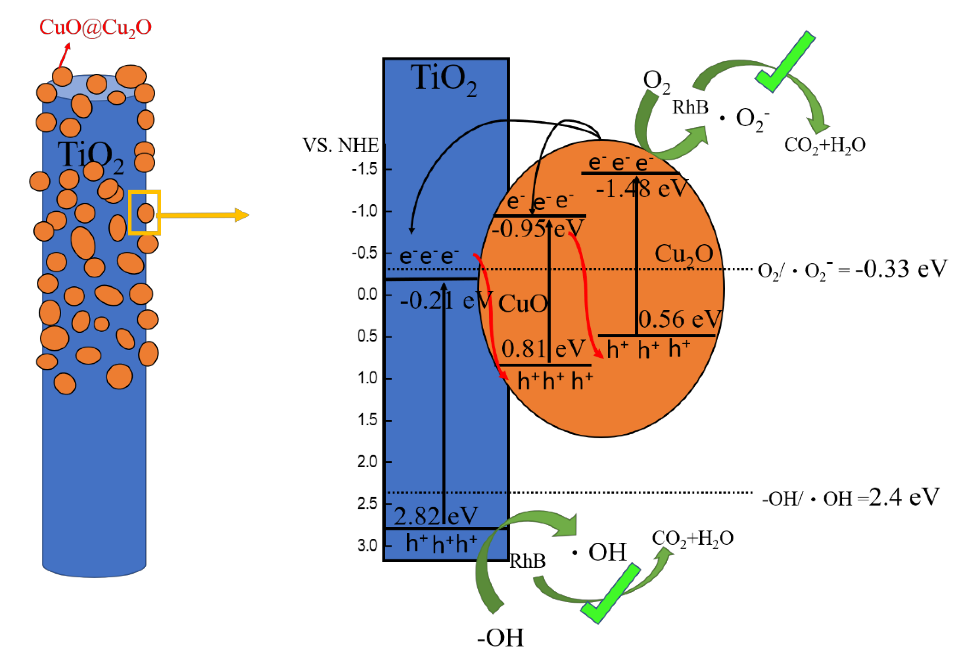
The band structures of pristine TiO2, Cu2O, and CuO were constructed according to the M-S measurements and the UV-vis analysis results, as shown in Figure 12. As shown in the previous scavenger experiments, the main active species involved in the TC350 photodegradation process with RhB solution were superoxide and hydroxyl radicals. Moreover, superoxide radicals demonstrated a greater contribution than hydroxyl radicals, as seen from the constructed band alignment in the ternary TC350 composite nanorods. If the electron–hole transfer route in the TC350 composite nanorods had followed the type II transfer mode, superoxide and hydroxyl radicals would not have been formed according to the relative band positions of the CB, VB, and redox potentials [62]. Therefore, none of the electrons/holes at the CB/VB positions would reach the required redox potential, so superoxide and hydroxyl active species would not have been produced with this mechanism. This contradicts the previous scavenger experiments. The Z-scheme mechanism shown in Figure 12 is more appropriate to explain the movement of photogenerated electrons/holes and the generation of active species for photodegradation. Under irradiation, photoinduced carriers form in the composite system (reaction 3). Through the movement of photogenerated carriers in the Z-scheme mechanism, the holes finally accumulated in the VB of TiO2 (2.82 eV vs. NHE), which was significantly higher than the oxidation potential of water or (–OH) molecules, which is 2.4 eV. Therefore, the holes were able to react with water (or –OH) molecules and generate hydroxyl radicals (reaction 4) [63]. In contrast, electrons accumulated in the CB of Cu2O (−1.48 eV vs. NHE). The electrons were located significantly lower than the reduction potential of oxygen (−0.33 eV), and electrons could react with oxygen to form superoxide radicals (reaction 5) [64]. These main reactive species could further react with RhB dye molecules and decompose into carbon dioxide and water (reaction 6) [65]:
Notably, from among the band alignments proposed for the TiO2, Cu2O, and CuO, multiple photoinduced charger transfer routes could occur in the ternary TiO2–Cu2O–CuO composite system. The p-n junctions formed between the n-type TiO2 and p-type copper oxides induced an internal electric field at the heterointerfaces, promoting charge separation under irradiation. The stepped-band edge arrangement in the composite system caused multiple Z-scheme transfer routes for the photoinduced charges. This finally resulted in the accumulation of holes at the VB of TiO2 and of electrons at the CB of Cu2O. A similar Z-scheme carrier movement was also exhibited in a ternary ZnO–Cu2O–CuO photocatalyst system [66]. In the report by Wei et al., the composite material TiO2–Cu2O showed carrier movement with a Z scheme under irradiation [67]. These examples echo the carrier movement mechanism proposed in this work. In addition, the Z-scheme charge transfer in the composite nanorods had an important contribution in preventing the photocorrosion of Cu2O. Photocorrosion has been demonstrated in previous work on single-phase Cu2O photocatalysts [68]. The Cu2O phase coupling with TiO2 (TC200) or TiO2–CuO (TC300 and TC350) in the composite system effectively guided the photoexcited electrons and holes accumulated in the Cu2O and inhibited photocorrosion. Therefore, a stable photocurrent curve could be observed in the previous photoresponse plots. This is supported by work on introducing a protective layer of TiO2 in Cu2O–CuO heterojunction films to prevent the photocorrosion effect [69]. The multiple charge transfer routes shown in Figure 12 explain the superior photoactive performance of TiO2–Cu2O–CuO composite systems (TC350 and TC300) among the various TC composite nanorods. Finally, it should be mentioned that TC350 exhibited better photoactivity than that of TC300. This can be attributed to optical absorption and the microstructural differences between the TC300 and TC350. The TC350 exhibited a better light absorption ability than TC300, as revealed by the previous UV-vis absorption analysis, which enhanced the generation efficiency of photoexcited charges in TC350. Moreover, TC350 also had a larger surface particle size in the decorated copper oxide layer in comparison to that of TC300. A larger grain size reduces grain boundaries in the decorated copper oxide layer, resulting in enhanced charge transport [47]. The ternary phase and suitable microstructural and optical properties of TC350 mean that it has excellent photoactivity compared to the other TC composite samples.
4. Conclusions
The morphology of copper oxide decorated on a TiO2 nanorod template changed from a continuous layer morphology to granular aggregates when the postannealing temperature was varied from 200 to 400 °C. The composite nanorods formed at 350 °C (TC350) exhibited superior photoactive performance compared to the other composite nanorods. The larger particle size resulting from the copper oxide modification in TC350 reduced the grain boundaries in the decorated layer, thereby increasing the charge transport ability. Moreover, the surface-modified Cu2O–CuO mixed crystallites on the TiO2 template could absorb sunlight more efficiently. These factors enhanced the photoactive performance of the TC350 composite nanorods studied herein. The scavenger tests demonstrated that the Z scheme was the possible carrier movement mechanism in TC350 under irradiation, and that result explains the high photocatalytic degradation ability of TC350 towards organic pollutants. The experimental results obtained herein demonstrate that regulation of the composition phase and microstructure of the modified copper oxide layer through control of the thermal annealing budget for the thin copper layer on TiO2 nanorod templates is a promising approach to design copper oxide–TiO2 composite nanorods with satisfactory photoactive performance.
Author Contributions
Methodology, Y.-C.L. and T.-H.L.; formal analysis, T.-H.L.; investigation, T.-H.L.; writing—original draft preparation, Y.-C.L. and T.-H.L.; supervision, Y.-C.L. All authors have read and agreed to the published version of the manuscript.
Funding
This research was funded by Ministry of Science and Technology of Taiwan, grant no. MOST 108-2221-E-019-034-MY3.
Data Availability Statement
Not applicable.
Conflicts of Interest
The authors declare no conflict of interest.
References
- Liang, Y.-C.; Zhao, W.-C. Morphology-dependent photocatalytic and gas-sensing functions of three-dimensional TiO2–ZnO nanoarchitectures. CrystEngComm 2020, 22, 7575–7589. [Google Scholar] [CrossRef]
- Wei, N.; Cui, H.; Wang, C.; Zhang, G.; Song, Q.; Sun, W.; Song, X.; Sun, M.; Tian, J. Bi2O3 nanoparticles incorporated porous TiO2 films as an effective p-n junction with enhanced photocatalytic activity. J. Am. Ceram. Soc. 2017, 100, 1339–1349. [Google Scholar] [CrossRef]
- Liang, Y.-C.; Chiang, K.-J. Coverage Layer Phase Composition-Dependent Photoactivity of One-Dimensional TiO2–Bi2O3 Composites. Nanomaterials 2020, 10, 1005. [Google Scholar] [CrossRef] [PubMed]
- Ravishankar, T.N.; Vaz, M.D.O.; Teixeira, S.R. The effects of surfactant in the sol–gel synthesis of CuO/TiO2 nanocomposites on its photocatalytic activities under UV-visible and visible light illuminations. New J. Chem. 2020, 44, 1888–1904. [Google Scholar] [CrossRef]
- Wang, M.; Sun, L.; Lin, Z.; Cai, J.; Xie, K.; Lin, C. p–n Heterojunction photoelectrodes composed of Cu2O-loaded TiO2 nanotube arrays with enhanced photoelectrochemical and photoelectrocatalytic activities. Energy Environ. Sci. 2013, 6, 1211–1220. [Google Scholar] [CrossRef]
- Liu, H.; Gao, L. Preparation and Properties of Nanocrystalline α-Fe2O3-Sensitized TiO2 Nanosheets as a Visible Light Photocatalyst. J. Am. Ceram. Soc. 2006, 89, 370–373. [Google Scholar] [CrossRef]
- Ye, M.; Pan, J.; Guo, Z.; Liu, X.; Chen, Y. Effect of ball milling process on the photocatalytic performance of CdS/TiO2 composite. Nanotechnol. Rev. 2020, 9, 558–567. [Google Scholar] [CrossRef]
- Lutz, T.; MacLachlan, A.; Sudlow, A.; Nelson, J.; Hill, M.S.; Molloy, K.C.; Haque, S.A. Thermal decomposition of solution processable metal xanthates on mesoporous titanium dioxide films: A new route to quantum-dot sensitised heterojunctions. Phys. Chem. Chem. Phys. 2012, 14, 16192–16196. [Google Scholar] [CrossRef]
- Ge, M.; Cao, C.; Li, S.; Zhang, S.; Deng, S.; Huang, J.; Li, Q.; Zhang, K.; Al-Deyab, S.S.; Lai, Y. Enhanced photocatalytic performances of n-TiO2 nanotubes by uniform creation of p–n heterojunctions with p-Bi2O3 quantum dots. Nanoscale 2015, 7, 11552–11560. [Google Scholar] [CrossRef]
- Shi, W.; Wang, J.C.; Chen, A.; Xu, X.; Wang, S.; Li, R.; Zhang, W.; Hou, Y. Cu Nanoparticles Modified Step-Scheme Cu2O/WO3 Heterojunction Nanoflakes for Visible-Light-Driven Conversion of CO2 to CH4. Nanomaterials 2022, 12, 2284. [Google Scholar] [CrossRef]
- Mizuno, K.; Izaki, M.; Murase, K.; Shinagawa, T.; Chigane, M.; Inaba, M.; Tasaka, A.; Awakura, Y. Structural and Electrical Characterizations of Electrodeposited p-Type Semiconductor Cu2O Films. J. Electrochem. Soc. 2005, 152, C179. [Google Scholar] [CrossRef]
- Wu, F.; Myung, Y.; Banerjee, P. Unravelling transient phases during thermal oxidation of copper for dense CuO nanowire growth. CrystEngComm 2014, 16, 3264–3267. [Google Scholar] [CrossRef]
- Wang, J.; Ji, G.; Liu, Y.; Gondal, M.; Chang, X. Cu2O/TiO2 heterostructure nanotube arrays prepared by an electrodeposition method exhibiting enhanced photocatalytic activity for CO2 reduction to methanol. Catal. Commun. 2014, 46, 17–21. [Google Scholar] [CrossRef]
- Shi, Q.; Ping, G.; Wang, X.; Xu, H.; Li, J.; Cui, J.; Abroshan, H.; Ding, H.; Li, G. CuO/TiO2 heterojunction composites: An efficient photocatalyst for selective oxidation of methanol to methyl formate. J. Mater. Chem. A 2019, 7, 2253–2260. [Google Scholar] [CrossRef]
- Park, S.M.; Razzaq, A.; Park, Y.H.; Sorcar, S.; Park, Y.; Grimes, C.A.; In, S.I. Hybrid CuxO–TiO2 Heterostructured Composites for Photocatalytic CO2 Reduction into Methane Using Solar Irradiation: Sunlight into Fuel. ACS Omega 2016, 1, 868–875. [Google Scholar] [CrossRef] [Green Version]
- Diachenko, O.; Kováč, J., Jr.; Dobrozhan, O.; Novák, P.; Kováč, J.; Skriniarova, J.; Opanasyuk, A. Structural and Optical Properties of CuO Thin Films Synthesized Using Spray Pyrolysis Method. Coatings 2021, 11, 1392. [Google Scholar] [CrossRef]
- Dai, M.-J.; Lin, S.-S.; Shi, Q.; Liu, F.; Wang, W.-X.; Chen, S.-C.; Kuo, T.-Y.; Sun, H. Transparent Conductive p-Type Cuprous Oxide Films in Vis-NIR Region Prepared by Ion-Beam Assisted DC Reactive Sputtering. Coatings 2020, 10, 473. [Google Scholar] [CrossRef]
- Nair, M.; Guerrero, L.; Arenas, O.L.; Nair, P. Chemically deposited copper oxide thin films: Structural, optical and electrical characteristics. Appl. Surf. Sci. 1999, 150, 143–151. [Google Scholar] [CrossRef]
- Mahendra, G.; Malathi, R.; Kedhareswara, S.P.; LakshmiNarayana, A.; Dhananjaya, M.; Guruprakash, N.; Hussain, O.M.; Mauger, A.; Julien, C.M. RF Sputter-Deposited Nanostructured CuO Films for Micro-Supercapacitors. Appl. Nano 2021, 2, 46–66. [Google Scholar] [CrossRef]
- Valladares, L.D.L.S.; Salinas, D.H.; Dominguez, A.B.; Najarro, D.A.; Khondaker, S.I.; Mitrelias, T.; Barnes, C.H.W.; Aguiar, J.A.; Majima, Y. Crystallization and electrical resistivity of Cu2O and CuO obtained by thermal oxidation of Cu thin films on SiO2/Si substrates. Thin Solid Film. 2012, 520, 6368–6374. [Google Scholar] [CrossRef]
- Serin, N.; Serin, T.; Horzum, Ş.; Celik, Y. Annealing effects on the properties of copper oxide thin films prepared by chemical deposition. Semicond. Sci. Technol. 2005, 20, 398–401. [Google Scholar] [CrossRef]
- Khojier, K.; Behju, A. Annealing Temperature Effect On Nanostructure And Phase Transition Of Copper Oxide Thin Films. Int. J. Nano Dimens. 2012, 2, 185–190. [Google Scholar]
- Liang, Y.-C.; Xu, N.-C.; Chiang, K.-J. Surface Morphology-Dependent Functionality of Titanium Dioxide–Nickel Oxide Nanocomposite Semiconductors. Nanomaterials 2019, 9, 1651. [Google Scholar] [CrossRef] [PubMed] [Green Version]
- Vidyasagar, C.C.; Naik, Y.A.; Venkatesha, T.G.; Viswanatha, R. Solid-State Synthesis and Effect of Temperature on Optical Properties of CuO Nanoparticles. Nano-Micro Lett. 2012, 4, 73–77. [Google Scholar] [CrossRef] [Green Version]
- Siqingaowa, Z.; Yao, H. Preparation and characterization of nanocrystalline ZnO by direct precipitation method. Front. Chem. China 2006, 1, 277–280. [Google Scholar] [CrossRef]
- Neumann, J.P.; Zhong, T.; Chang, Y.A. The Cu−O (Copper-Oxygen) system. Bull. Alloy. Phase Diagr. 1984, 5, 136–140. [Google Scholar] [CrossRef]
- Adilov, S.; Afanaciev, V.P.; Kashkul, I.N.; Kumekov, S.; Mukhin, N.V.; Terukov, E.I. Studying the Composition and Structure of Films Obtained by Thermal Oxidation of Copper. Glass Phys. Chem. 2017, 43, 272–275. [Google Scholar] [CrossRef]
- Akkari, F.C.; Kanzari, M.; Rezig, B. Preparation and characterization of obliquely deposited copper oxide thin films. Eur. Phys. J. Appl. Phys. 2007, 40, 49–54. [Google Scholar] [CrossRef]
- Johan, M.R.; Suan, M.S.M.; Hawari, N.L.; Ching, H.A. Annealing Effects on the Properties of Copper Oxide Thin Films Prepared by Chemical Deposition. Int. J. Electrochem. Sci. 2011, 6, 6094–6104. [Google Scholar]
- Dong, K.; He, J.; Liu, J.; Li, F.; Yu, L.; Zhang, Y.; Zhou, X.; Ma, H. Photocatalytic performance of Cu2O-loaded TiO2/rGO nanoheterojunctions obtained by UV reduction. J. Mater. Sci. 2017, 52, 6754–6766. [Google Scholar] [CrossRef]
- Datye, A.K.; Xu, Q.; Kharas, K.C.; McCarty, J.M. Particle size distributions in heterogeneous catalysts: What do they tell us about the sintering mechanism? Catal. Today 2006, 111, 59–67. [Google Scholar] [CrossRef]
- Lim, Y.F.; Chua, C.S.; Lee, C.J.J.; Chi, D. Sol–gel deposited Cu2O and CuO thin films for photocatalytic water splitting. Phys. Chem. Chem. Phys. 2014, 16, 25928–25934. [Google Scholar] [CrossRef]
- Wang, Y.; Lü, Y.; Zhan, W.; Xie, Z.; Kuang, Q.; Zheng, L. Synthesis of Porous Cu2O/CuO Cages using Cu-based Metal-Organic-Framework as Templates and their Gas-sensing Properties. J. Mater. Chem. A 2015, 3, 12796–12803. [Google Scholar] [CrossRef]
- Khan, M.A.; Nayan, N.; Ahmad, M.K.; Soon, C.F. Surface Study of CuO Nanopetals by Advanced Nanocharacterization Techniques with Enhanced Optical and Catalytic Properties. Nanomaterials 2020, 10, 1298. [Google Scholar] [CrossRef]
- Dubale, A.A.; Pan, C.-J.; Tamirat, A.G.; Chen, H.-M.; Su, W.-N.; Chen, C.-H.; Rick, J.; Ayele, D.W.; Aragaw, B.A.; Lee, J.-F.; et al. Heterostructured Cu2O/CuO decorated with nickel as a highly efficient photocathode for photoelectrochemical water reduction. J. Mater. Chem. A 2015, 3, 12482–12499. [Google Scholar] [CrossRef]
- Liang, Y.-C.; Liu, Y.-C. Design of Nanoscaled Surface Morphology of TiO2–Ag2O Composite Nanorods through Sputtering Decoration Process and Their Low-Concentration NO2 Gas-Sensing Behaviors. Nanomaterials 2019, 9, 1150. [Google Scholar] [CrossRef] [Green Version]
- Liang, Y.-C.; Wang, C.-C. Hydrothermally derived zinc sulfide sphere-decorated titanium dioxide flower-like composites and their enhanced ethanol gas-sensing performance. J. Alloy. Compd. 2018, 730, 333–341. [Google Scholar] [CrossRef]
- Hamad, H.; Elsenety, M.M.; Sadik, W.; El-Demerdash, A.G.; Nashed, A.; Mostafa, A.; Elyamny, S. The superior photocatalytic performance and DFT insights of S-scheme CuO@TiO2 heterojunction composites for simultaneous degradation of organics. Sci. Rep. 2022, 12, 2217. [Google Scholar] [CrossRef]
- Wang, S.; Huo, R.; Zhang, R.; Zheng, Y.; Li, C.; Pan, L. Synthesis of core–shell N-TiO2@CuOx with enhanced visible light photocatalytic performance. RSC Adv. 2018, 8, 24866–24872. [Google Scholar] [CrossRef] [Green Version]
- Musa, A.; Akomolafe, T.; Carter, M. Production of cuprous oxide, a solar cell material, by thermal oxidation and a study of its physical and electrical properties. Sol. Energy Mater. Sol. Cells 1998, 51, 305–316. [Google Scholar] [CrossRef]
- Deng, X.; Wang, C.; Shao, M.; Xu, X.; Huang, J. Low-temperature solution synthesis of CuO/Cu2O nanostructures for enhanced photocatalytic activity with added H2O2: Synergistic effect and mechanism insight. RSC Adv. 2017, 7, 4329–4338. [Google Scholar] [CrossRef] [Green Version]
- Nakatani, K.; Himoto, K.; Kono, Y.; Nakahashi, Y.; Anma, H.; Okubo, T.; Maekawa, M.; Kuroda-Sowa, T. Synthesis, Crystal Structure, and Electroconducting Properties of a 1D Mixed-Valence Cu(I)–Cu(II) Coordination Polymer with a Dicyclohexyl Dithiocarbamate Ligand. Crystals 2015, 5, 215–225. [Google Scholar] [CrossRef] [Green Version]
- Balık, M.; Bulut, V.; Erdogan, I.Y. Optical, structural and phase transition properties of Cu2O, CuO and Cu2O/CuO: Their photoelectrochemical sensor applications. Int. J. Hydrog. Energy 2019, 44, 18744–18755. [Google Scholar] [CrossRef]
- Hsu, Y.-K.; Yu, C.-H.; Chen, Y.-C.; Lin, Y.-G. Synthesis of novel Cu2O micro/nanostructural photocathode for solar water splitting. Electrochim. Acta 2013, 105, 62–68. [Google Scholar] [CrossRef]
- Masudy-Panah, S.; Radhakrishnan, K.; Tan, H.R.; Yi, R.; Wong, T.I.; Dalapati, G.K. Ten It Wong, Goutam Kumar Dalapati, Titanium doped cupric oxide for photovoltaic application. Sol. Energy Mater. Sol. Cells 2015, 140, 266–274. [Google Scholar] [CrossRef]
- Dong, Y.; Tao, F.; Wang, L.; Lan, M.; Zhang, J.; Hong, T. One-pot preparation of hierarchical Cu2O hollow spheres for improved visible-light photocatalytic properties. RSC Adv. 2020, 10, 22387–22396. [Google Scholar] [CrossRef]
- Jeong, D.; Jo, W.; Jeong, J.; Kim, T.; Han, S.; Son, M.-K.; Jung, H. Characterization of Cu2O/CuO heterostructure photocathode by tailoring CuO thickness for photoelectrochemical water splitting. RSC Adv. 2022, 12, 2632–2640. [Google Scholar] [CrossRef]
- Liang, Y.C.; Chou, Y.H. Matrix phase induced boosting photoactive performance of ZnO nanowire turf-coated Bi2O3 plate composites. J. Am. Ceram. Soc. 2021, 104, 5432–5444. [Google Scholar] [CrossRef]
- Kmentova, H.; Henrotte, O.; Yalavarthi, R.; Haensch, M.; Heinemann, C.; Zbořil, R.; Schmuki, P.; Kment, Š.; Naldoni, A. Nanoscale Assembly of BiVO4/CdS/CoOx Core–Shell Heterojunction for Enhanced Photoelectrochemical Water Splitting. Catalysts 2021, 11, 682. [Google Scholar] [CrossRef]
- Huang, W.; Li, W.-X. Surface and interface design for heterogeneous catalysis. Phys. Chem. Chem. Phys. 2019, 21, 523–536. [Google Scholar] [CrossRef]
- Zheng, D.; Yu, L.; Liu, W.; Dai, X.; Niu, X.; Fu, W.; Shi, W.; Wu, F.; Cao, X. Structural advantages and enhancement strategies of heterostructure water-splitting electrocatalysts. Cell Rep. Phys. Sci. 2021, 2, 100443. [Google Scholar] [CrossRef]
- Cong, Y.; Ge, Y.; Zhang, T.; Wang, Q.; Shao, M.; Zhang, Y. Fabrication of Z-Scheme Fe2O3–MoS2–Cu2O Ternary Nanofilm with Significantly Enhanced Photoelectrocatalytic Performance. Nd. Eng. Chem. Res. 2018, 57, 881–890. [Google Scholar] [CrossRef]
- Liang, Y.-C.; Wang, Y.-P. Optimizing crystal characterization of WO3–ZnO composites for boosting photoactive performance via manipulating crystal formation conditions. CrystEngComm 2021, 23, 3498–3509. [Google Scholar] [CrossRef]
- Bengas, R.; Lahmar, H.; Redha, K.M.; Mentar, L.; Azizi, A.; Schmerber, G.; Dinia, A. Electrochemical synthesis of n-type ZnS layers on p-Cu2O/n-ZnO heterojunctions with different deposition temperatures. RSC Adv. 2019, 9, 29056–29069. [Google Scholar] [CrossRef] [Green Version]
- Zhang, Y.; Yi, Z.; Wu, G.; Shen, Q. Novel Y doped BiVO4 thin film electrodes for enhanced photoelectric and photocatalytic performance. J. Photochem. Photobiol. A Chem. 2016, 327, 25–32. [Google Scholar] [CrossRef]
- Jang, J.S.; Kim, H.G.; Lee, J.S. Heterojunction semiconductors: A strategy to develop efficient photocatalytic materials for visible light water splitting. Catal. Today 2012, 185, 270–277. [Google Scholar] [CrossRef]
- Chen, H.; Leng, W.; Xu, Y. Enhanced Visible-Light Photoactivity of CuWO4 through a Surface-Deposited CuO. J. Phys. Chem. C 2014, 118, 9982–9989. [Google Scholar] [CrossRef]
- Peng, B.; Zhang, S.; Yang, S.; Chen, H.; Wang, H.; Yu, H.; Zhang, S.; Peng, F. Synthesis and characterization of g-C3N4/Cu2O composite catalyst with enhanced photocatalytic activity under visible light irradiation. Mater. Res. Bull. 2014, 56, 19–24. [Google Scholar] [CrossRef]
- Peng, B.; Zhang, S.; Yang, S.; Wang, H.; Yu, H.; Zhang, S.; Peng, F. The facile hydrothermal synthesis of CuO@ZnO heterojunction nanostructures for enhanced photocatalytic hydrogen evolution. New J. Chem. 2019, 43, 6794–6805. [Google Scholar]
- Aguilera-Ruiz, E.; De La Garza-Galván, M.; Zambrano-Robledo, P.; Ballesteros-Pacheco, J.C.; Vazquez-Arenas, J.; Peral, J.; García-Pérez, U.M. Facile synthesis of visible-light-driven Cu2O/BiVO4 composites for the photomineralization of recalcitrant pesticides. RSC Adv. 2017, 7, 45885–45895. [Google Scholar] [CrossRef] [Green Version]
- Liang, Y.C.; Chiang, K.J. Design and tuning functionality of rod-like titanium dioxide–nickel oxide composites via a combinational methodology. Nanotechnology 2020, 31, 195709. [Google Scholar] [CrossRef] [PubMed]
- Jiang, X.; Lai, S.; Xu, W.; Fang, J.; Chen, X.; Beiyuan, J.; Zhou, X.; Lin, K.; Liu, J.; Guan, G. Novel ternary BiOI/g-C3N4/CeO2 catalysts for enhanced photocatalytic degradation of tetracycline under visible-light radiation via double charge transfer process. J. Alloy. Compd. 2019, 809, 151804. [Google Scholar] [CrossRef]
- Aguirre, M.E.; Zhou, R.; Eugene, A.J.; Guzman, M.I.; Grela, M.A. Cu2O/TiO2 heterostructures for CO2 reduction through a direct Z-scheme: Protecting Cu2O from photocorrosion. Appl. Catal. B Environ. Vol. 2017, 217, 485–493. [Google Scholar] [CrossRef]
- Dasineh Khiavi, N.; Katal, R.; Kholghi Eshkalak, S.; Masudy-Panah, S.; Ramakrishna, S.; Jiangyong, H. Visible Light Driven Heterojunction Photocatalyst of CuO–Cu2O Thin Films for Photocatalytic Degradation of Organic Pollutants. Nanomaterials 2019, 9, 1011. [Google Scholar] [CrossRef] [Green Version]
- Xu, X.; Sun, Y.; Fan, Z.; Zhao, D.; Xiong, S.; Zhang, B.; Zhou, S.; Liu, G. Mechanisms for ·O−2 and OH Production on Flowerlike BiVO4 Photocatalysis Based on Electron Spin Resonance. Front. Chem. 2018, 6, 64. [Google Scholar] [CrossRef] [Green Version]
- Yoo, H.; Kahng, S.; Kim, J.H. Z-scheme assisted ZnO/Cu2O-CuO photocatalysts to increase photoactive electrons in hydrogen evolution by water splitting. Sol. Energy Mater. Sol. Cells 2020, 204, 110211. [Google Scholar] [CrossRef]
- Wei, T.; Zhu, Y.N.; An, X.; Liu, L.M.; Cao, X.; Liu, H.; Qu, J. Defect Modulation of Z-Scheme TiO2/Cu2O Photocatalysts for Durable Water Splitting. ACS Catal. 2019, 9, 8346–8354. [Google Scholar] [CrossRef]
- Huang, L.; Peng, F.; Yu, H.; Wang, H. Preparation of cuprous oxides with different sizes and their behaviors of adsorption, visible-light driven photocatalysis and photocorrosion. Solid State Sci. 2009, 11, 129–138. [Google Scholar] [CrossRef]
- Wang, P.; Wen, X.; Amal, R.; Ng, Y.H. Introducing a protective interlayer of TiO2 in Cu2O–CuO heterojunction thin film as a highly stable visible light photocathode. RSC Adv. 2015, 5, 5231–5236. [Google Scholar] [CrossRef]
Figure 1.
SEM images: (a) TiO2, (b) TC200, (c) TC300, (d) TC350, and (e) TC400. Corresponding Cu, O, and Ti mapping images of the composite nanorods: (f) TC200, (g) TC300, (h) TC350, and (i) TC400.
Figure 1.
SEM images: (a) TiO2, (b) TC200, (c) TC300, (d) TC350, and (e) TC400. Corresponding Cu, O, and Ti mapping images of the composite nanorods: (f) TC200, (g) TC300, (h) TC350, and (i) TC400.

Figure 2.
XRD patterns: (a) TC200, (b) TC300, (c) TC350, and (d) TC400.
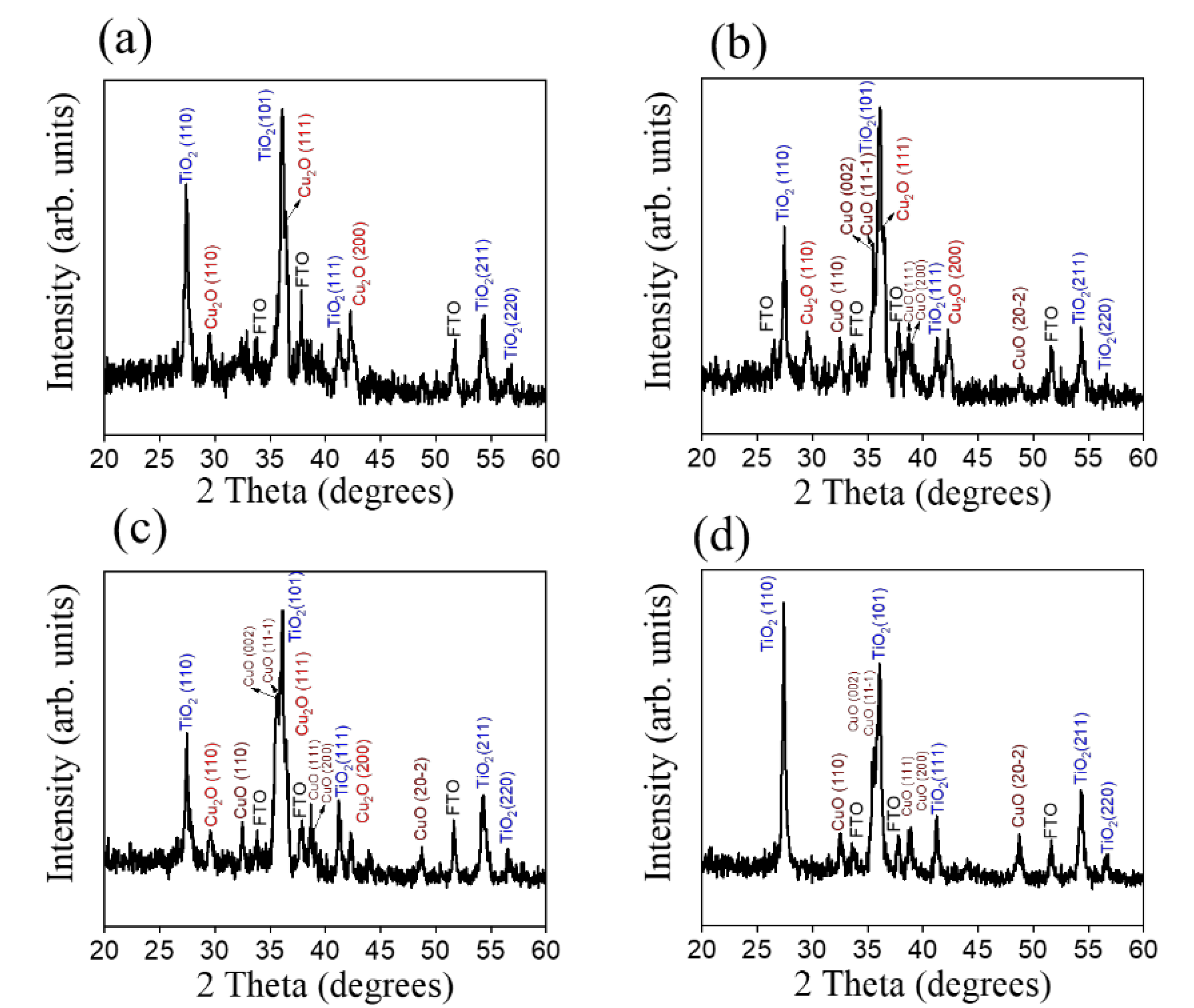
Figure 3.
TEM analysis of TC200: (a) low-magnification TEM image; (b,c) HRTEM images of various regions of the composite rod as marked in (a); (d) SAED patterns of several TC200 nanorods; (e) EDS line scanning profiles across the composite rod.
Figure 3.
TEM analysis of TC200: (a) low-magnification TEM image; (b,c) HRTEM images of various regions of the composite rod as marked in (a); (d) SAED patterns of several TC200 nanorods; (e) EDS line scanning profiles across the composite rod.

Figure 4.
TEM analysis of TC350: (a) low-magnification TEM image; (b,c) HRTEM images of various regions of the composite rod as marked in (a); (d) SAED patterns of several TC350 nanorods; (e) EDS line scanning profiles across the composite rod.
Figure 4.
TEM analysis of TC350: (a) low-magnification TEM image; (b,c) HRTEM images of various regions of the composite rod as marked in (a); (d) SAED patterns of several TC350 nanorods; (e) EDS line scanning profiles across the composite rod.

Figure 5.
TEM analysis of TC400: (a) low-magnification TEM image; (b,c) HRTEM images of various regions of the composite rod as marked in (a); (d) SAED patterns of several TC400 nanorods; (e) EDS line scanning profiles across the composite rod.
Figure 5.
TEM analysis of TC400: (a) low-magnification TEM image; (b,c) HRTEM images of various regions of the composite rod as marked in (a); (d) SAED patterns of several TC400 nanorods; (e) EDS line scanning profiles across the composite rod.
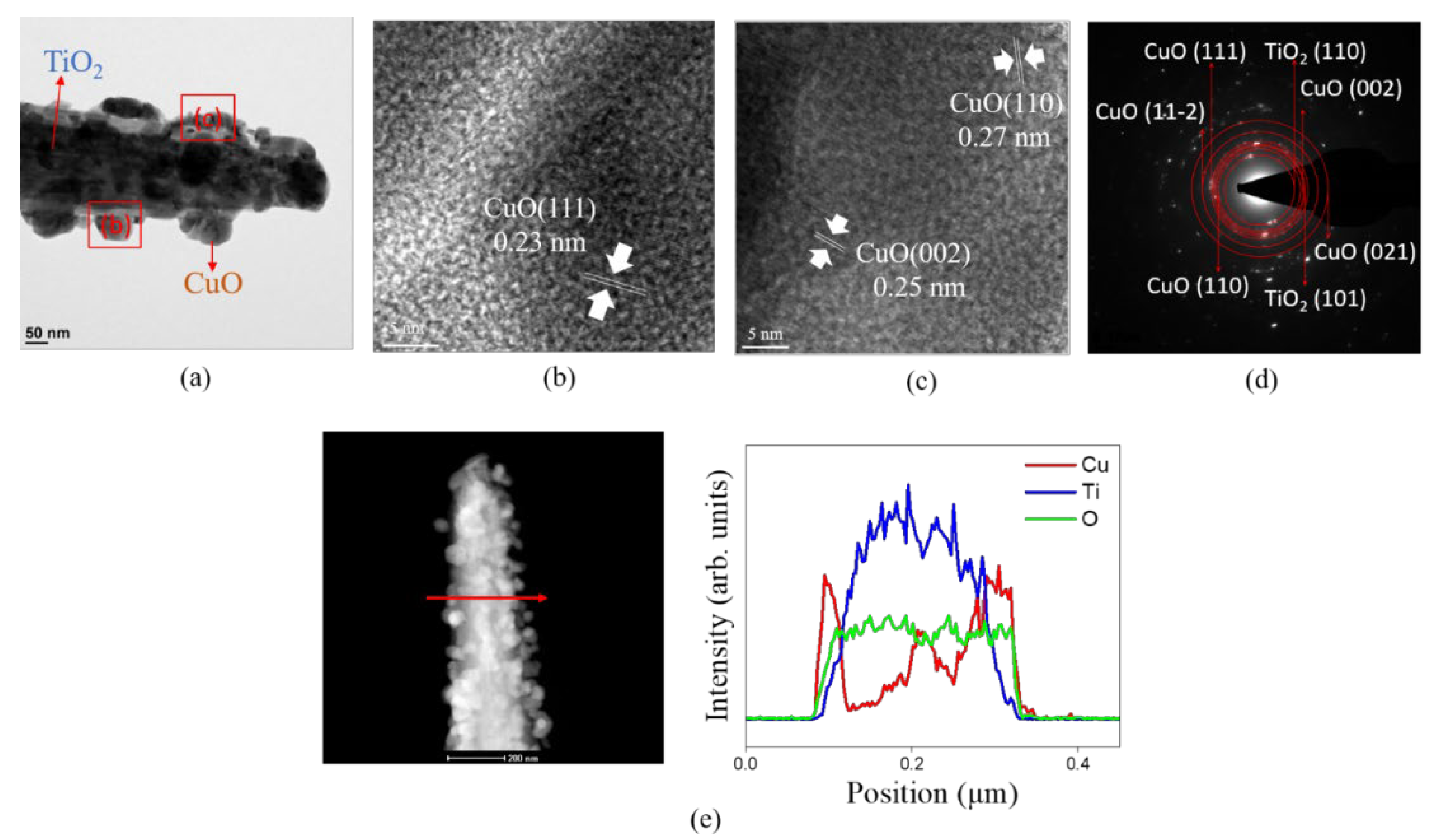
Figure 6.
High-resolution XPS Cu 2p spectra: (a) TC200, (b) TC350, and (c) TC400.
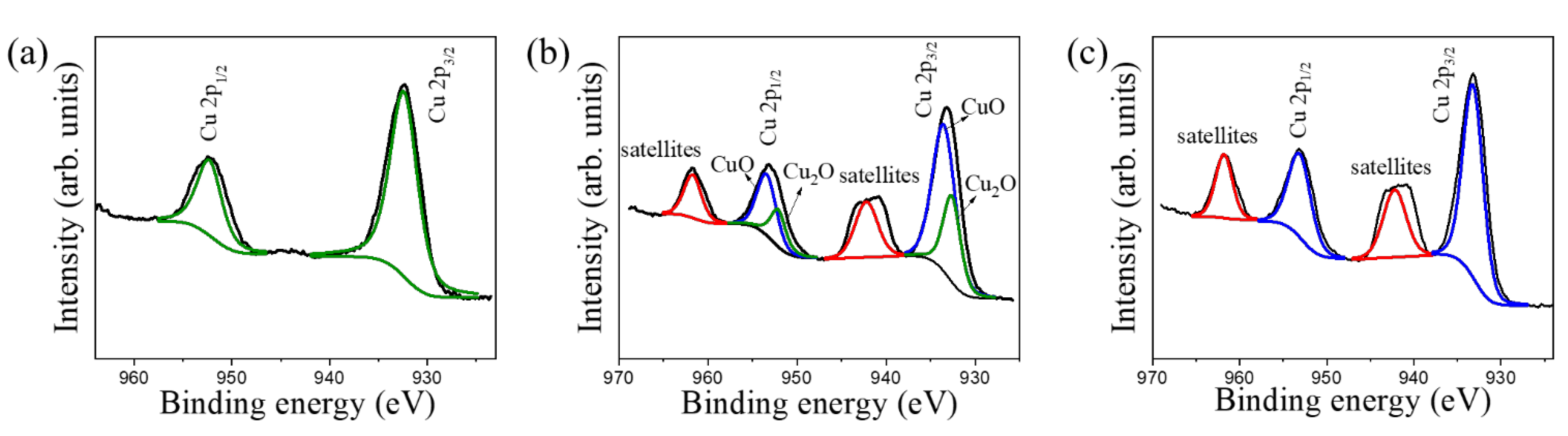
Figure 7.
High-resolution XPS Ti 2p spectra: (a) TiO2 and (b) comparison of Ti 2p spectra of various samples.
Figure 7.
High-resolution XPS Ti 2p spectra: (a) TiO2 and (b) comparison of Ti 2p spectra of various samples.
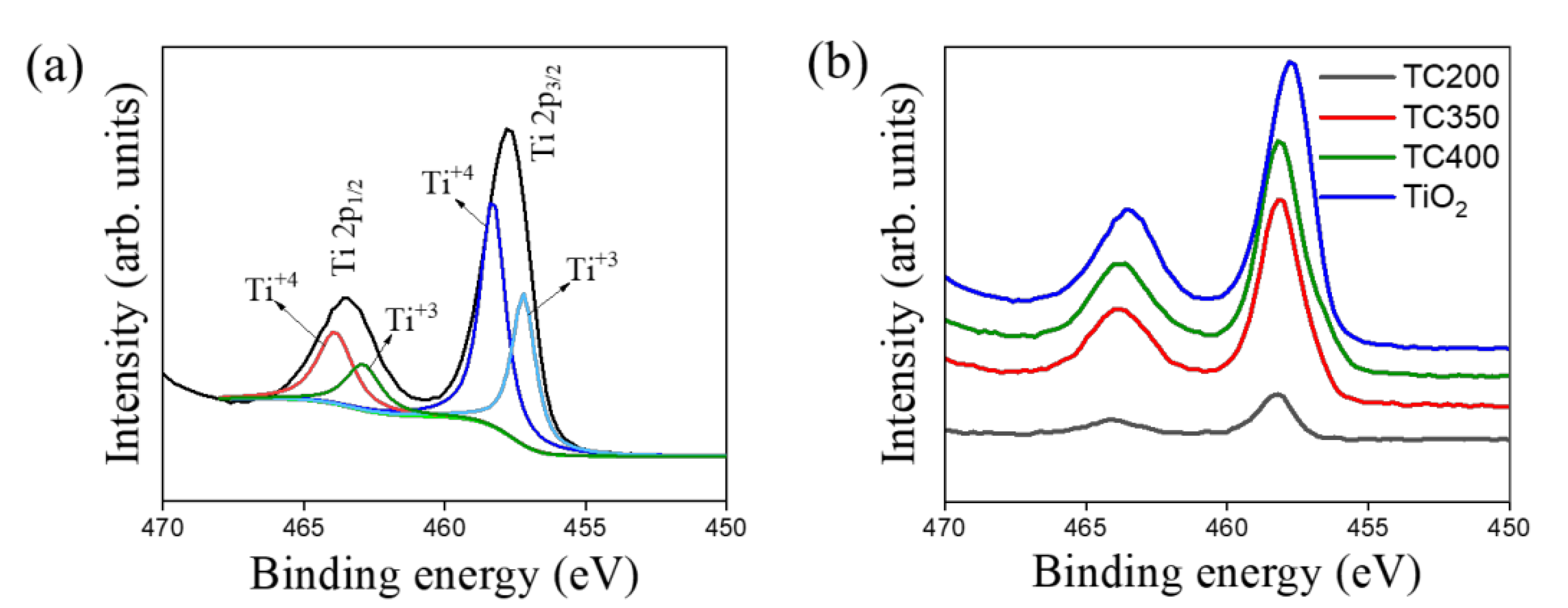
Figure 8.
(a) Absorption spectra of various samples and Band-gap evaluations of (b) various nanorod samples, (c) pristine Cu2O and CuO films.
Figure 8.
(a) Absorption spectra of various samples and Band-gap evaluations of (b) various nanorod samples, (c) pristine Cu2O and CuO films.
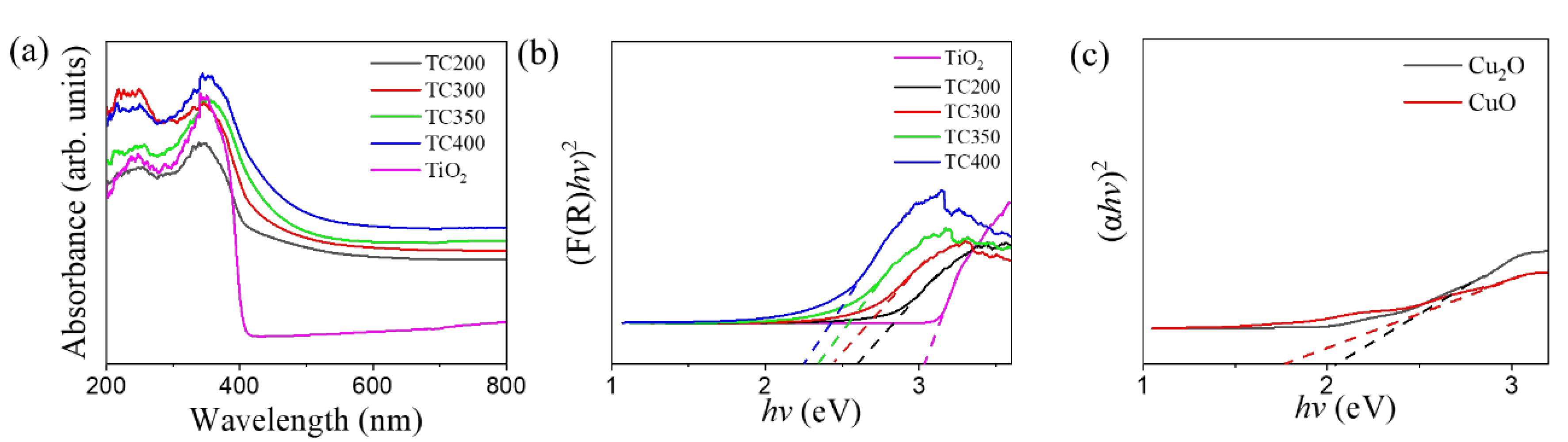
Figure 9.
(a) Photocurrent density versus time curves for various samples at 1.2 V (vs. Ag/AgCl) under chopping illumination. (b) Nyquist plots for various samples under irradiation. (c) Possible equivalent circuits for Rct evaluation.
Figure 9.
(a) Photocurrent density versus time curves for various samples at 1.2 V (vs. Ag/AgCl) under chopping illumination. (b) Nyquist plots for various samples under irradiation. (c) Possible equivalent circuits for Rct evaluation.

Figure 10.
Mott–Schottky plots for various samples: (a) TiO2, (b) Cu2O, and (c) CuO. (d) A series of M−S plots for various composite nanorods.
Figure 10.
Mott–Schottky plots for various samples: (a) TiO2, (b) Cu2O, and (c) CuO. (d) A series of M−S plots for various composite nanorods.

Figure 11.
(a) C/Co vs. irradiation duration plots; (b) ln (Co/C) vs. irradiation duration plots; (c) degradation percentages of RhB solution with TC350 in the presence of various scavengers.
Figure 11.
(a) C/Co vs. irradiation duration plots; (b) ln (Co/C) vs. irradiation duration plots; (c) degradation percentages of RhB solution with TC350 in the presence of various scavengers.
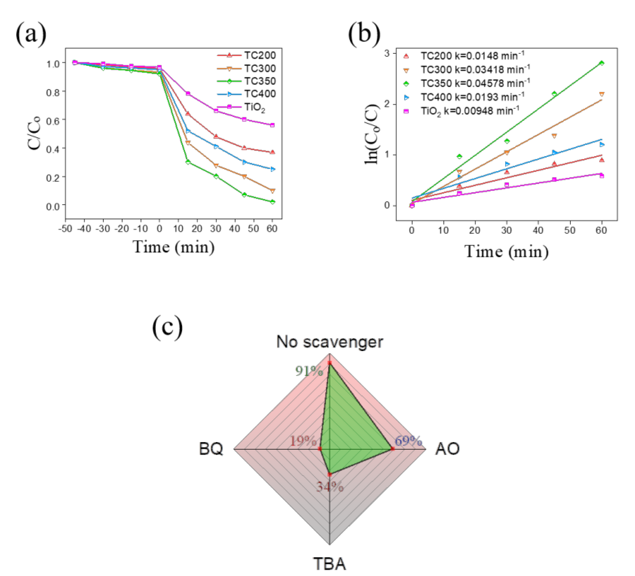
Figure 12.
Possible mechanisms of charge transfer in TC350 under irradiation.
Publisher’s Note: MDPI stays neutral with regard to jurisdictional claims in published maps and institutional affiliations. |
© 2022 by the authors. Licensee MDPI, Basel, Switzerland. This article is an open access article distributed under the terms and conditions of the Creative Commons Attribution (CC BY) license (https://creativecommons.org/licenses/by/4.0/).
Share and Cite
MDPI and ACS Style
Liang, Y.-C.; Li, T.-H. Sputtering-Assisted Synthesis of Copper Oxide–Titanium Oxide Nanorods and Their Photoactive Performances. Nanomaterials 2022, 12, 2634. https://doi.org/10.3390/nano12152634
AMA Style
Liang Y-C, Li T-H. Sputtering-Assisted Synthesis of Copper Oxide–Titanium Oxide Nanorods and Their Photoactive Performances. Nanomaterials. 2022; 12(15):2634. https://doi.org/10.3390/nano12152634
Chicago/Turabian StyleLiang, Yuan-Chang, and Tsun-Hsuan Li. 2022. "Sputtering-Assisted Synthesis of Copper Oxide–Titanium Oxide Nanorods and Their Photoactive Performances" Nanomaterials 12, no. 15: 2634. https://doi.org/10.3390/nano12152634
Note that from the first issue of 2016, this journal uses article numbers instead of page numbers. See further details here.