Review

Review of Electrochemically Synthesized Resistive Switching Devices: Memory Storage, Neuromorphic Computing, and Sensing Applications

1
Computational Electronics and Nanoscience Research Laboratory, School of Nanoscience and Biotechnology, Shivaji University, Kolhapur 416004, India
2
School of Electrical Engineering, Korea University, Anam-dong, Seoul 02841, Republic of Korea
3
Department of Electronics, Shivaji University, Kolhapur 416004, India
4
Department of Physics, Dr. Homi Bhabha State University, 15, Madam Cama Road, Mumbai 400032, India
5
Department of Convergence Electronic Engineering, Gyeongsang National University, Jinjudae-ro 501, Jinju 52828, Republic of Korea
6
Department of Electronics, Osan University, 45, Cheonghak-ro, Osan-si 18119, Republic of Korea
*
Authors to whom correspondence should be addressed.
Nanomaterials 2023, 13(12), 1879; https://doi.org/10.3390/nano13121879
Submission received: 3 April 2023 / Revised: 9 June 2023 / Accepted: 13 June 2023 / Published: 17 June 2023
(This article belongs to the Special Issue Advances in Memristive Nanomaterials)

Abstract

:
Resistive-switching-based memory devices meet most of the requirements for use in next-generation information and communication technology applications, including standalone memory devices, neuromorphic hardware, and embedded sensing devices with on-chip storage, due to their low cost, excellent memory retention, compatibility with 3D integration, in-memory computing capabilities, and ease of fabrication. Electrochemical synthesis is the most widespread technique for the fabrication of state-of-the-art memory devices. The present review article summarizes the electrochemical approaches that have been proposed for the fabrication of switching, memristor, and memristive devices for memory storage, neuromorphic computing, and sensing applications, highlighting their various advantages and performance metrics. We also present the challenges and future research directions for this field in the concluding section.

1. Introduction

The key to the development of powerful, energy-efficient neuromorphic computer systems lies in the fabrication of electronic devices that can imitate biological synapses. In this context, the efficiency bottlenecks that occur in the conventional computation of neural algorithms have driven the development of novel devices capable of performing in-memory computing. As a result, energy-efficient neuromorphic systems with resistive memory are expected to eventually replace the prevalent Von Neumann computing architecture [1]. Neuromorphic computing emulates the neural networks of the human brain, utilizing neural/synaptic devices that act as processors and memories to process large amounts of data with low energy requirements. The primary motivation for the development of this technology has been the exponential growth of data in recent decades. Data are regarded as the fuel of the new economy and represent a source of wealth in the knowledge era, particularly because they have been generated more rapidly as technology has advanced via multiple sources, including human interactions, electronic media, social networks, machines, and historical archives [2]. The efficient storage and processing of big data have thus taken on greater importance, particularly due to the insights that can be gained from identifying underlying patterns within the data. Therefore, the present review addresses the storage of data and the emergence of neuromorphic computing and sensing applications utilizing resistive switching (RS) devices.
The fabrication of efficient data storage devices for various applications has received significant attention from researchers worldwide [1,3]. One of the noteworthy trends in recent years has been the emergence of memory devices based on memristors, referred to as the fourth fundamental circuit element and pioneered by Prof. Chua [4]. It should be noted that conventional RS devices are also referred to as memristor/memristive devices, meaning these terms can be used interchangeably [5]. In addition to memristive-based memory, solid-state memory devices have become more widespread in the past decade, including those based on resistive random access memory (RRAM) [6], phase-change memory (PCM) [7], magnetoresistive random access memory [8], conductive bridging random access memory [9], and ferroelectric random access memory [10]. Memory devices have also been increasingly employed in both digital computing (as digital gates [11], reconfigurable logic circuits, and crossbar arrays [12]) and analog applications (including neuromorphic computing [13], oscillators [14], amplifiers [15], filters [16], chaotic circuits [17], sensors [18], optical devices [19,20], and thermoelectric devices [21,22]).
Because of the increasing demands for data storage and information-processing devices for both consumer and industrial applications, recent research has targeted devices with high speed, high memory density, low power consumption, and a small environmental footprint [3]. Accordingly, various physical and chemical deposition techniques have been developed to fabricate RS devices. Commonly used physical deposition techniques include sputtering, atomic layer deposition, e-beam deposition, and pulsed laser deposition. However, given that cost-effectiveness and ease of solution processability are crucial for the fabrication of RS devices, chemical approaches have become more widespread, including hydrothermal methods [23,24], spray deposition [25], SILAR [26], spin coating [27,28], drop-casting [29], microwave [30], screen printing [31,32], doctor blading, and electrochemical methods [33]. In terms of the direction and advancement of RS performance, it is essential to comprehend the impact of synthesis procedures, including the cost. Additionally, synthesis procedures must be defined with regard to their compatibility with complementary metal-oxide semiconductors (CMOSs) and practical deployment. Therefore, it is imperative to conduct a rigorous analysis of the various synthesis techniques present in the literature to enable improvements in device merits.
Electrochemically synthesized RS devices have been reported to exhibit excellent RS performance. Moreover, electrochemical synthesis has several advantages over other chemical synthesis techniques, including a high production rate, low cost, industrial applicability, accurate control over morphology, the possibility of multilayered growth, no requirement for post-deposition treatment, and low operating temperatures [34]. The most widely used electrochemical approaches for the synthesis of thin films are electrodeposition, electrophoretic deposition, and anodization. In these processes, an external electric stress is applied between two electrodes that are immersed in an electrolyte containing ionic species, charged particles, and/or etching agents [35,36,37]. For example, electrodeposition is based on the oxidation and reduction of ionic species due to an external potential/current, with the target material deposited on the working electrode [35]. Electrochemical approaches also allow for variation in the synthesis parameters (such as the applied electric current and deposition time) to induce structural changes in the synthesized material. In addition, the electrolyte concentration, pH, and temperature can be adjusted to modulate the composition of materials and the morphology [38]. This tunability facilitates the fabrication of high-performance RS devices using electrochemical techniques. The primary advantages of electrochemical synthesis are the ability to control the switching layer size using the bottom-up approach, ionic transport, ease of fabrication, and industrial applicability, rendering this technique suitable for state-of-the-art RS devices.
Given the dramatic increase in the volume of data generated due to technological advances and associated scaling issues, the present review focuses on memory, neuromorphic, and sensor applications based on electrochemically fabricated RS devices. The review provides basic information on RS devices, various synthesis techniques, and application domains for researchers. Moreover, this review article is helpful to determine which synthesis technique is beneficial for future research in RS devices. In particular, the present article provides important research directions for electrochemically synthesized RS devices in terms of memory, neuromorphic computing, and sensing applications. Finally, this review recommends future guidelines for electrochemically synthesized high-performance RS devices. The first section of the review provides a general introduction to memory devices, while Section 2 contains a description of the RS effect (and its mechanisms) and a discussion on unipolar and bipolar RS. The details of RS devices and their applications are then discussed in Section 3, while Section 4 focuses on memory storage, neuromorphic and sensing devices, and the fabrication techniques employed for RS devices. A summary of electrochemical techniques is provided in Section 5, including electrodeposition, anodization, and electrophoretic deposition. Subsequently, Section 6 presents a description of electrochemically synthesized RS materials for memory storage applications, including carbon, zinc oxide (ZnO), copper oxide (Cu2O), titanium oxide (TiO2), and other metal oxides. Section 7 and Section 8 summarize electrochemically synthesized RS materials for neuromorphic computing and sensing applications, respectively. Finally, the future outlook is summarized in Section 9, and the conclusions are presented in Section 10.

2. Resistive Switching Effects

The RS effect is typically observed in metal/insulator or semiconductor/metal devices, in which the insulator or semiconductor material is sandwiched between the top and bottom metal electrodes (Figure 1a) [39]. RS is a unique property of nano- and micromaterials where the electrical resistivity of a material can take on multiple stable states in accordance with the applied voltage [39,40,41,42,43,44]. The applied voltage induces the migration of either oxygen vacancies or metal ions, which forms conducting filaments within the device and tunes the resistance of the switching layer. Figure 1b presents the general steps involved in the RS process [40]. In the electroforming process, a high voltage is applied to the device for a short time to create conductive filaments from oxygen vacancies or metal ions. Most researchers prefer to employ electroforming to initiate the RS process in a device [45], which can lead to both volatile and non-volatile memory effects. For example, Hu et al. reported a Pt/InGaZnO/W device with volatile RS memory without electroforming and stable bipolar RS after electroforming [46]. After the electroforming process, a relatively low SET voltage can put the device into a low-resistance state (LRS) due to the formation of complete conductive filaments, while the subsequent use of a RESET voltage switches the device to a high-resistance state (HRS), in which the conductive filaments are ruptured [47,48,49].

2.1. Unipolar and Bipolar Resistive Switching

RS devices can be classified as unipolar or bipolar depending on the polarity of the SET and RESET voltages and their current–voltage (I–V) characteristics. As shown in Figure 1c [41], in unipolar RS devices, switching occurs at the same polarity, while a bias of the opposite polarity is required for bipolar RS devices [50]. In unipolar RS devices, the Joule effect is one of the main causes of the dissolution of the conductive filaments during the RESET process [51]; thus, these devices can be switched using voltages with the same polarity. In contrast, in bipolar RS devices, the dissolution of conductive filaments occurs due to the migration of oxygen vacancies or metal ions during the RESET process. It is possible for some RS devices to exhibit both unipolar and bipolar modes [52,53], with the device structure [54,55] and operating setup [56] affecting the switching mode of the device.
Endurance is an important characteristic of an RS device and is defined as the number of times the device switches between two or more stable resistance states (i.e., SET/RESET transitions) with an appropriate ON/OFF ratio or memory window (Figure 1d) [3]. Endurance can be measured experimentally in a number of ways, such as recording the I–V sweep, current-visible pulsed voltage stress (PVS), and current-blind PVS [3,57]. Similarly, data retention is a measure of the long-term stability of the LRS and HRS (Figure 1e) [42]. In non-volatile RS devices, it is crucial to retain data for an extended period. In general, the minimum acceptable data retention time is 10 years [3]. Another important characteristic of RS devices is the switching time (Figure 1f) [43], which is the time required for a device to transition from an LRS to an HRS or vice versa. According to technical requirements, the switching time between SET and RESET should be less than 10 ns per transition in either direction [3]. This high-speed switching ensures the rapid execution of any task.

2.2. Resistive Switching Mechanisms

The RS mechanisms for electrochemical metallization memory (ECM), valance-change memory (VCM), thermochemical memory (TCM), and PCMP are presented in Figure 2 [58,59,60,61]. The following subsections cover the general details of each RS mechanism.

2.2.1. Electrochemical Metallization Memory

Electrochemical redox reactions play a crucial role in ECM devices, with metal oxidation and reduction within the switching layer leading to the formation and rupture of conduction filaments [40]. In particular, when a positive bias is applied to the top electrode (i.e., the anode), metal cations are generated that migrate to the bottom electrode (i.e., the cathode), where they are reduced to form conductive filaments. This switches the device to the SET process (i.e., an LRS). The RESET process (i.e., an HRS) is achieved by Joule heating or by applying a bias of the opposite polarity to the memory device, which oxidizes the reduced cations, leading to their migration back to the anode. Figure 2a presents an ECM device with Cu as the top electrode and highly doped Si as the bottom electrode [22]. A positive bias switches the device to an ON state via the migration of Cu+ ions to the bottom electrode, which is reduced to form conduction filaments. The opposite polarity switches the device to an OFF state by moving the Cu+ ions back to the Cu electrode [22]. ECM devices offer several advantages, such as lower SET/RESET voltages and lower power consumption, compared to VCM-type devices while also offering rapid switching times (close to a nanosecond scale) and a high ON/OFF ratio due to the complete dissolution of the conduction filaments [62].
Figure 2. (a) Schematic representation of I–V sweeping, including the formation and dissolution of a conduction filament in electrochemical metallization memory (ECM). Reprinted with permission from [22]. Copyright © 2023, Elsevier B.V. (b) Schematic representation of the electroforming, SET and RESET process in valance-change memory (VCM) due to the migration of oxygen vacancies. Reprinted with permission from [59]. Copyright © 2023, Springer-Nature. (c) Schematic representation of the SET and RESET process in thermochemical memory (TCM) [63]. Copyright © 2023, De Gruyter. (d) Diagrammatic representation of the amorphous and crystalline state of the cell in phase-change memory (PCM) [61]. Copyright © 2023, Springer-Nature.
Nanomaterials 13 01879 g002

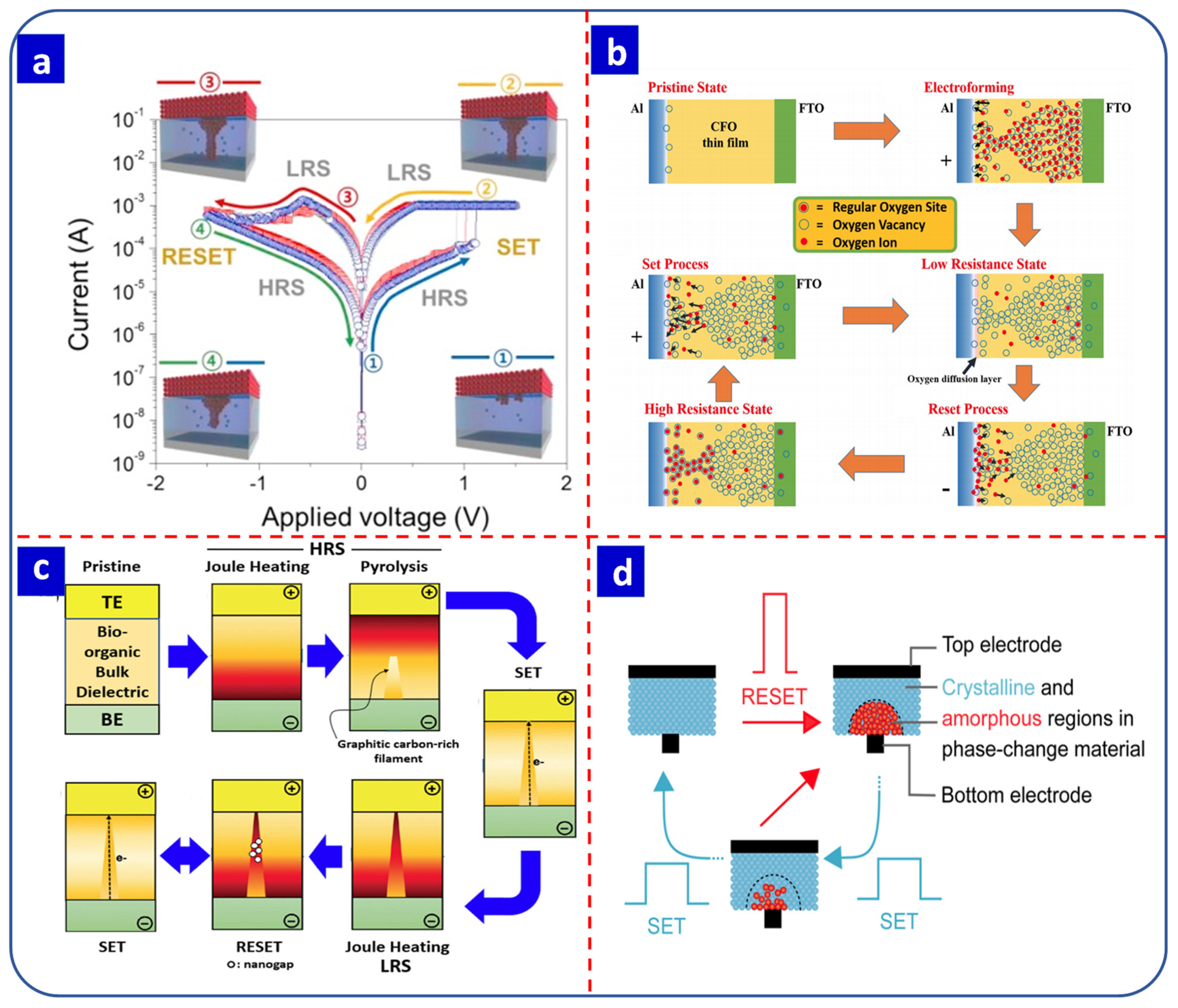
2.2.2. Valance-Change Memory

In VCM, oxygen vacancies play a vital role in the RS process. The migration of oxygen vacancies and oxygen ions due to the applied electric field is responsible for the SET and RESET process [62]. RS occurs when a positive bias is applied to the anode, which results in the movement of oxygen vacancies toward the cathode, which acts as an electron acceptor. At the same time, oxygen ions move towards the anode, which switches the device to an LRS by creating oxygen vacancies based on the conductive filaments. On the other hand, the opposite polarity switches the device to an HRS by inserting oxygen ions back into the oxygen sites. The typical VCM-based RS process for an Al/CoFe2O4/FTO device is presented in Figure 2b [59]. The oxygen vacancy channel is formed during electroforming by applying a high voltage between the top and bottom electrodes. Due to the applied electroforming voltage, oxygen anions migrate towards the positively biased top electrode, leaving behind oxygen vacancies. A sufficient number of oxygen vacancies forms conduction filaments between the two electrodes during the SET process. When a reverse bias is applied, the oxygen anions return and fill the oxygen vacancies near the top electrode, producing an HRS [59]. Compared to ECM cells, VCM cells operate at a higher voltage and thus dissipate more power. However, the retention of a VCM cell is much higher than that of an ECM cell. On the other hand, VCM cells generally have a lower ON/OFF ratio than ECM cells [62].

2.2.3. Thermochemical Memory

TCM is generally the least preferred RS mechanism. Typically, TCM devices exhibit unipolar RS, and the formation and rupture of the conduction filaments are dependent on thermal energy and the Joule effect [58]. In the RESET process, an appropriately high current increases the temperature of the conduction filaments due to the Joule heating effect (Figure 2c) [60,62,63]. Russo et al. reported the simulation analysis of a NiO RS device and the effect of the temperature of conductive filaments on RS properties [60].

2.2.4. Phase-Change Memory

PCM is widely used in non-volatile memory storage devices. In PCM cells, the phase of the switching material (i.e., crystalline or amorphous) is tuned by applying external voltage pulses [64,65]. The resistivity of the amorphous phase is higher than the crystalline phase, allowing for data storage in the form of 1′s and 0′s (Figure 2d) [61]. In the RESET process, applying a large electric pulse to the crystalline material for a short time causes a heating effect that increases the temperature of the switching layer; subsequent rapid cooling leads to an amorphous structure. During the SET process, a medium electric pulse is required to heat the material above the crystallization temperature for a relatively long time to switch the device from an HRS to an LRS [64,66,67]. GeSbTe-based devices employ this phase-change mechanism and exhibit a high endurance of 2 × 10¹² cycles [68]. Recently, electrochemically fabricated GeSbTe-based PCM devices with excellent non-volatile memory properties have also been reported [69].

3. Resistive Switching Devices and Their Applications

RS devices are widely employed for memory storage [70], neuromorphic [1], and sensing [71] applications (Figure 3). Many metal-oxide-based resistive devices have been studied in recent years due to their unique physical, chemical, and electrical properties that allow them to be employed for memory storage, neuromorphic electronics, logic gate, and sensor applications [72,73,74]. In the following sections, various applications for RS devices are described [75].

3.1. Memory Storage

Efficient data storage is a crucial requirement for modern technology, with many memory storage designs having been developed in recent decades. Of these, RRAM devices are the most attractive [73]. A schematic representation of an Al/Ti3C2Tx-TiO2/Pt RS memory device is presented in Figure 3a, with its I–V characteristics shown in Figure 3b and its endurance and retention properties summarized in Figure 3c,d, respectively [28].
The technological requirements for RS devices in memory storage applications are summarized in Table 1. In RS memory storage devices, switching the resistance from an HRS to an LRS and vice versa can be used to store data in the form of 0′s and 1′s, respectively [76]. Memory storage devices require low reading and writing voltages, with some RS devices reported to have an operating voltage of 0.5 V with a low power consumption of 0.1 pJ per transition [77]. For practical applications, the endurance of a device should be greater than 109 cycles, with many RS devices achieving up to 1012 cycles [57], and its data retention time should approach 10 years, though a recent report for an RS device shows data retention time higher than this [78]. The switching time is also an essential factor for memory storage devices, with a switching time of fewer than 10 ns recently reported for RS-based devices [79]. In addition, the demand for miniaturized memory devices has grown recently, with Govoreanu et al. fabricating a few nanometer-sized RS cells [77]. To date, the most frequently researched materials for memory storage applications have been transition metal oxides [80], metal nitrides [81,82], carbon-based materials [83], polymers [84], and chalcogenides [85,86].

3.2. Neuromorphic Computing

Neuromorphic computing seeks to emulate brain functions using electronic devices. The human brain is composed of billions of neurons, with synapses controlling their connections. At a basic level, memory and learning are controlled by pre-neurons, synapses, and post-neurons. Typically, a signal is transferred as an electrical spike from a pre-neuron to a post-neuron via a synapse. When the pre-neuron receives the signal, transmitters are generated in the vesicles, and depolarization of the pre-neuron opens the channel, through which the transmitters reach a receptor in the post-neuron by passing through a 20–40 nm long synaptic cleft [1]. In the case of artificial synapses, the properties of a biological synapse are emulated using metal/insulator/metal RS devices, with the top and bottom electrodes acting as the pre-neuron and post-neuron, respectively, and the switching layer or insulator acting as the synapse. For the more accurate mimicking of synaptic properties, analog RS-based devices are generally used, with metal oxides [1], perovskites [87], polymers [88], organic materials [89], and 2D nanomaterials [90] being widely used for RS-based neuromorphic computing applications. A schematic representation of biological and electrical synapses based on RS devices is presented in Figure 3e [86].
Table 1. The technology requirements of RS devices for memory storage, neuromorphic computing, and sensor applications.
RequirementsRefs.
Memory storageOperating voltage<1 V[3,76,77,78,79]
Type of switchingDigital, analog
Switching layer thickness50 nm
Power consumption~10 pJ/transition
Switching time<10 ns/transition
Endurance>109 cycles
Data retention>10 years (85 °C)
MIM cell size~500 nm2
3D stackingYes
Neuromorphic computingOperating voltage<1 V[1,2,91]
Type of switchingAnalog
Switching layer thickness50 nm
Power consumption~10 pJ/transition
Switching time<10 ns/transition
Endurance>109 cycles
Data retention>10 years
MIM cell size~500 nm2
Potentiation and depression (P&D)Yes
Spike-timing-dependent plasticity (STDP)Yes
Spike-rate-dependent plasticity (SRDP)Yes
SensorOperating voltage<1 V[3,75]
Type of switchingDigital, analog
Switching layer thickness50 nm
Power consumption~10 pJ/transition
Switching time<10 ns/transition
Endurance>109 cycles
Data retention>10 years (85 °C)
MIM cell size~500 nm2
Response timeLow as possible
Synaptic plasticity is an essential property of the human brain that is associated with modifications in the synaptic weight, which is the strength between two neurons. Spike-timing-dependent plasticity (STDP) and spike-rate-dependent plasticity (SRDP) are the two main variants of synaptic plasticity [1]. Positive and negative values for the synaptic weight represent potentiation and depression, respectively, which can further be classified into short-term potentiation (STP), long-term potentiation (LTP), short-term depression (STD), and long-term depression (LTD) [91], all of which facilitate information storage and learning. STD involves a temporary rise in the synaptic weight followed by an abrupt decline to the original state. In LTD, a permanent change in the synaptic weight occurs following repeated input pulses [91]. A temporal decay in the negative synaptic value indicates STD, while LTD is identified by a permanently low negative synaptic weight [1,91]. The potentiation–depression and antisymmetric Hebbian learning rules of a Ag/a-BN/Pt memristor device are displayed in Figure 3f,g, respectively [82].
The fabrication of electronic devices to mimic synaptic properties (such as STD and LTD) remains challenging. Recently, many electronic devices have been reported that mimic basic and advanced brain functionalities, including RS-based memory devices [92], transistors [93], and ferroelectric junctions [94]. However, the current electronic synaptic devices generally have high power/energy consumption, unstable potentiation and depression dynamics, and unstable conduction states. In addition, the non-linearity and fewer resistive states of artificial synaptic devices have become bottlenecks, affecting the realization of high-performance neuromorphic computing systems. Therefore, further research is required to overcome these challenges and produce efficient artificial synapses. The technological requirements for RS devices in neuromorphic computing applications are summarized in Table 1.

3.3. Sensor Applications

RS devices can be employed in both sensors and detectors [75,95]. Most resistance-based sensing devices operate based on a change in resistance induced by a change in the properties of the constituent materials. In RS-based electrochemical sensors, the oxidation and reduction of constituent materials in accordance with the applied voltage and presence of the analyte are monitored [96]. In this context, the change in the resistance from an LRS to an HRS (or vice versa), switching voltage, hysteresis area, and memory window are important physical parameters for RS-based sensors. In particular, when an RS device comes into contact with a target analyte, one or more of these physical parameters will generally change, and monitoring this change allows the device to be employed as a sensor. A representative RS-based sensor is presented in Figure 3h–j [75]. In this case, the change in the current over time and in response to the concentration of the analyte when applying an appropriate voltage shows that resistive materials can respond to the analyte and switch to a different resistive state [75]. The analyte can thus be analyzed quantitatively or qualitatively based on the gap in the voltage or the change in RS properties [49]. The technological requirements for RS devices in sensor applications are summarized in Table 1.

3.4. Other Applications

Other applications that can employ RS memory characteristics include thermoelectric [21,22] and optical devices [97]. These are applications for solving the trade-off between conductivity and transmittance [98,99] (Figure 3k–m).
Figure 3. (a) Schematic illustration of an Al/Ti3C2Tx-TiO2/Pt RS device for memory storage applications. (b) I–V characteristics of the device. (c) Endurance and (d) retention properties of the device. Reprinted with permission from [28]. Copyright © 2023, published by Elsevier. (e) A schematic representation of biological and electrical synapses. Reprinted with permission from [86]. Copyright © 2023, published by Elsevier B.V. (f,g) Neuromorphic properties, potentiation, and depression behaviors of a Ag/a-BN/Pt memristor device. Reprinted with permission from [82]. Copyright © 2023, American Chemical Society. (h) Schematic representation of an IrOx/Al2O3/TaOx/MoS2/TiN device for ascorbic acid (AA) detection. (i) Current vs. response time curves for this device at buffer and different AA concentrations. (j) Current change vs. AA concentration (1 pM to 1 μM) measured using this device. Reprinted with permission from [75]. Copyright © 2023, American Chemical Society. (k) Schematic of electric-field-driven metal implantation for electrode fabrication. Reprinted with permission from [97]. Copyright © 2023, Springer Nature. (l) Schematic illustration of an AlGaN-based DUV light-emitting diode. Reprinted with permission from [98]. Copyright © 2023, IEEE. (m) Electric-field-induced doping treatment process and thermal stability of the current paths formed in a GaOx electrode. Reprinted with permission from [99]. Copyright © 2023, Elsevier B.V.
Nanomaterials 13 01879 g003

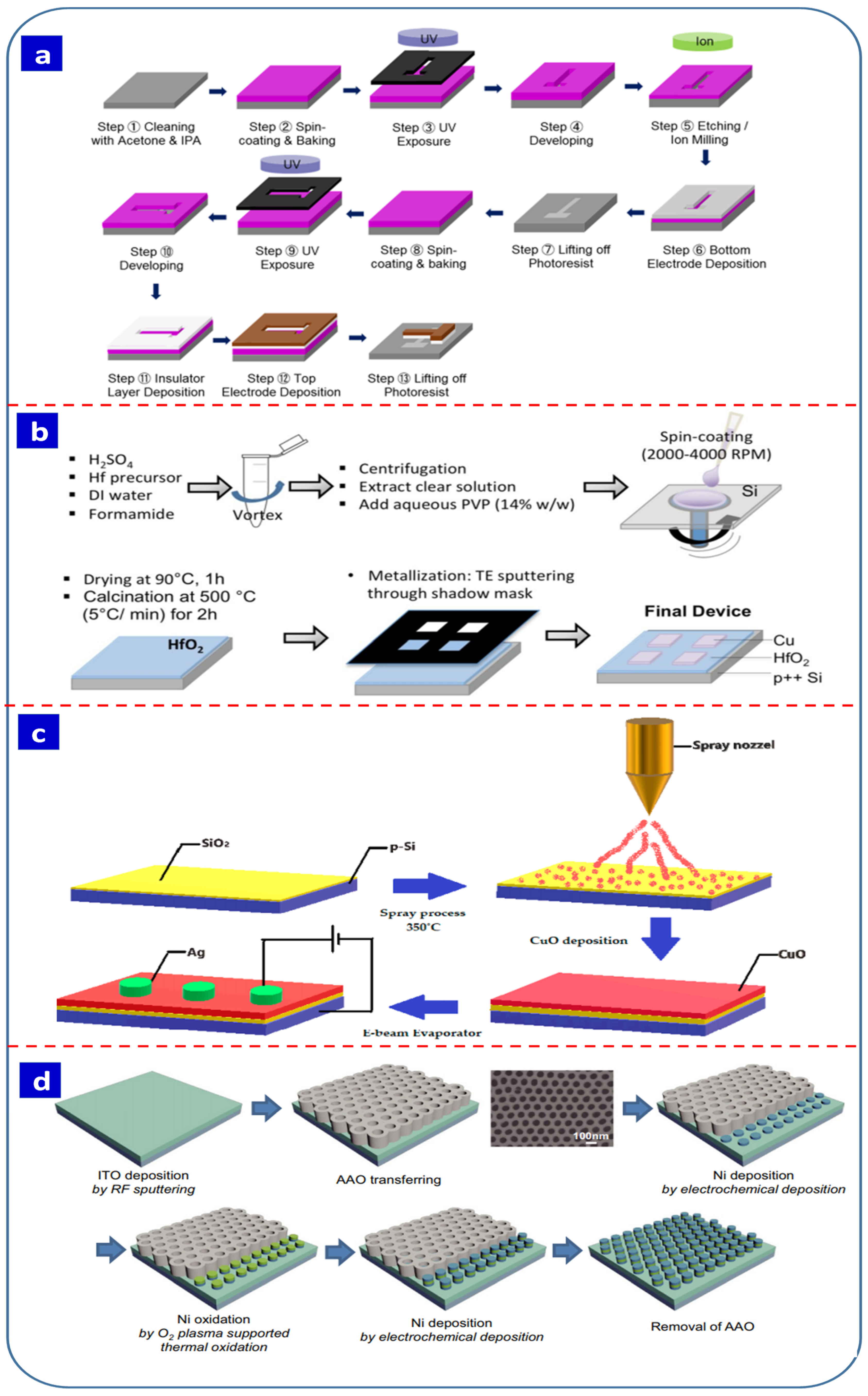
4. Fabrication Techniques for Resistive Switching Devices

The method employed to fabricate a device will affect its RS properties [100,101,102], with the same material potentially demonstrating different RS behavior when synthesized using different approaches [103,104]. Thus, various factors such as industrial practicality, cost-effectiveness, and RS performance need to be considered when fabricating an RS device. Techniques such as sputtering [105,106,107], lithography [108], spin coating [109], spray pyrolysis [110], and electrodeposition [104] have previously been reported for the synthesis of the active switching layer in RS devices, while hydrothermal [111], dip coating [112], SILAR [26], electrospinning [113], and many other solution-processable techniques [114,115] have also been developed for the same purpose. For the top and bottom electrodes, physical deposition techniques are utilized; thus, this section focuses on the options for the fabrication of the active layer.
The advantages and disadvantages of switching layer synthesis techniques are summarized in Table 2 [116,117,118,119,120]. Physical fabrication techniques such as sputtering, atomic layer deposition, and pulsed layer deposition are precise and suitable for industrial applications. However, they are costly and require many steps to fabricate cost-effective RS devices, while their high operating temperatures, requirement for a vacuum, and inability to control the morphology are also limitations. For example, as presented in Figure 4a, the fabrication process for a Pt/HfO2/Ti RRAM device involves two-step lithography, etching, and deposition processes that are quite complex [100]. Similarly, chemical vapor deposition requires an inert atmosphere and high temperatures. In contrast, spin coating, hydrothermal fabrication, and spray pyrolysis represent cost-effective and easy fabrication approaches. However, spin-coated and hydrothermally synthesized thin films have lower adhesion and durability than physical vapor deposition and are thus not suitable for large-scale deposition. Figure 4b presents the process for the preparation of a spin-coated Cu/HfO2/p++ Si device [27]. The high synthesis temperature required for these techniques is also a disadvantage. Figure 4c presents the steps involved in the fabrication of a Ag/CuO/SiO2/p-Si RS device, which involves the deposition of a CuO thin film on a SiO2 substrate using spray pyrolysis and the deposition of the top electrode using e-beam evaporation [101].
Figure 4d presents an anodized aluminum oxide (AAO) template-based electrochemical approach for RS device fabrication [102]. Electrochemical synthesis techniques generally involve a simple fabrication process and are industrially feasible, inexpensive, environmentally friendly, do not require high temperatures, and produce consistent growth over a large surface area. Moreover, they allow precise control of the film thickness and achieve high switching quality through adjustment of the synthesis parameters. In addition, the adherence and durability of electrochemically synthesized thin films are significantly higher than those with other solution-processable techniques. Electrochemical approaches can also be used to fabricate the entire metal–insulator–metal device, while template-assisted deposition and nanostructured devices can be achieved with electrochemical synthesis. Some reports have also suggested that electrochemically synthesized devices have superior properties compared with sol–gel and spin-coated devices [103,104]. The advantages and disadvantages of the synthesis methods are summarized in Table 2 [116,117,118,119,120]. The thickness of the switching layer can also affect the RS properties of the end device, and electrochemical synthesis allows the deposition of a very thin switching layer with controlled morphology. For example, the minimum thickness of a switching layer achieved using electrodeposition is 15–20 nm [121].
Various criteria should be considered when comparing the RS performance of memory devices made using diverse fabrication technologies, such as the thicknesses of the switching and top and bottom electrode layers, the choice of top and bottom electrodes, and the synthesis methods because they all have an influence on the RS characteristics. We analyzed the RS performance of various copper oxide-based devices by considering the previously mentioned factors while focusing on industrially applicable techniques that are cost-effective with a simple synthesis process, as summarized in Table 2. From the table, it is evident that electrochemically synthesized copper oxide-based devices are switched at a low voltage (0.7 V), similar to RS devices fabricated using a sputtering process (VSET: 0.7 V and VRESET: −0.5 V). In addition, devices made using these techniques exhibited endurance greater than 103 cycles and retention up to 103 s, while devices fabricated using other methods achieved relatively poor RS performance [104,105,106,107,108,109,110,111,112,113,114,115,116,117,118,119,120]. These results indicate that the electrochemical method can provide excellent RS performance, similar to sputtering and other physical synthesis procedures.

5. Electrochemical Methods for Resistive Switching Devices

5.1. Electrodeposition
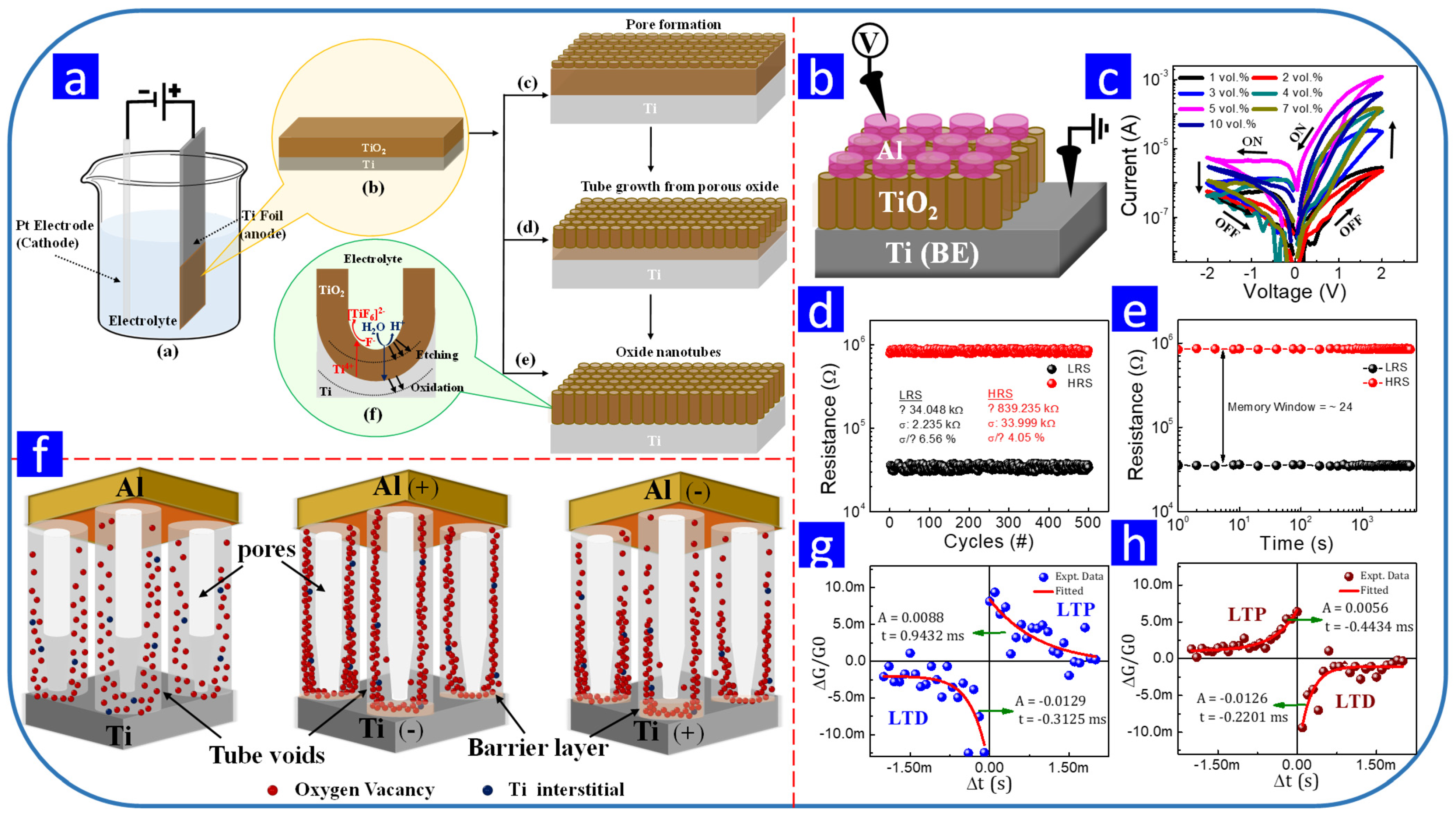
Electrochemical synthesis is an elegant and versatile technique that allows the controlled deposition of an electrolyte onto conducting material with the application of an electric current or voltage across two electrodes [122]. Electrochemical synthesis can be classified as cathodic and anodic electrodeposition [123]. In cathodic electrodeposition, charged species, clusters, and nanoparticles are deposited on the cathode. Depending on the deposited charged species, charged particles, and applied power, electrodeposition can be classified as electroplating, electrophoretic, or electroless deposition. In electroplating, metal cations in the electrolyte move towards the cathode due to an external electric field and are reduced on the surface of the cathode (Figure 5a). Most semiconductors, chalcogenides, and oxide-based thin films can be fabricated using this technique.
In electrophoretic deposition, similar reaction mechanisms can occur, but it does not involve any chemical reaction, i.e., the reduction of ionic species. Instead, the driving force for this technique depends on the charge and electrophoretic mobility of the particles involved. The electrolyte is replaced by a suspension of charged particles in an organic solvent [123]. This technique can be used to deposit charged particles, nanomaterials [124,125], and carbon-based materials [126]. Figure 5b presents the general mechanisms for electrophoretic deposition. Dispersed charged particles in the organic solvent are attracted or deposited on the oppositely charged conducting electrode following the application of an external DC voltage/current. Electrophoretic deposition can be both cathodic and anodic [127].
In electroless deposition, deposition occurs without any external electric supply. This is an autocatalytic process in which redox reactions occur due to reducing agents that act as a source of electrons (Figure 5c) [123,128]. The electrode is dipped in an electrolyte containing reducing agents and metal precursors. The autocatalytic redox reactions deposit metal atoms on the electrode by removing the metal atoms on the electrode surface. This deposition technique provides a simple and cost-effective path for the decoration of metals such as Sn, Au, and Ni or nanoparticles on metal-oxide thin films [129,130] and is highly selective.
Electrochemically prepared thin films can be deposited in a potentiostatic or galvanostatic manner, in which the current density varies with a constant voltage and the electrode potential varies with a constant current, respectively. Chronoamperometry, chronopotentiometry, and voltammetric deposition are also common thin-film synthesis techniques [104]. In electrochemical fabrication, several parameters should be considered for the uniform deposition of thin films, including the electrolyte concentration, applied electric field, pH, deposition time, deposition temperature, and distance between the two electrodes [131,132]. The thickness of the deposited film is controlled by tuning the deposition time and the applied electric field, while pH and the deposition temperature are responsible for compositional changes in the deposited materials [38]. In addition, the distance between the two electrodes can determine the structure and morphology of the thin film.
Figure 5. (a) Schematic representation of electrodeposition using a two-electrode system. (b) Schematic representation of electrophoretic deposition and (c) electroless deposition. (d) Schematic representation of anodization. (e) Influence of the electric field strength on the activation energy for the migration of ions during anodization. Reprinted with permission from [132]. Copyright © 2023, Royal Society of Chemistry.
Nanomaterials 13 01879 g005

5.2. Anodization

Anodization is a widely used technique for the preparation of high-quality thin films for the fabrication of electronic devices due to its large-scale fabrication capabilities and simplicity [131,132,133]. In the anodization process, the metal anode is electrochemically oxidized. Figure 5d presents the metal anode as a reservoir of infinite metal cations (Mz+/Ny+) with an electrolyte reservoir of infinite anions (O2−/An−) [132]. The applied electrical potential oxidizes the cations on the surface of the anode, which forms a thin oxide film on the surface of the anode. The thickness of the oxide layer is directly proportional to the applied electric field, which triggers the ionic conductivity of the oxide on the surface of the metal. Three theories have been proposed to explain the rate-determining steps: Verwey’s theory, which proposes that ion transfer within the oxide film is responsible for the metal-oxide thin film [134], Mott-Cabrera’s theory, which posits that ion transfer across the metal–oxide interface and determines the thickness of the film [135], and Dewald’s theory, which highlights the influence of ion transfer across the oxide–electrolyte interface [136]. The high field mechanism explains the exponential dependency of the current density (i) on the electric field strength (E), as given in Equation (1) [132].
  i   = N ν q exp   W α a q E k B T
where N is the surface density of mobile ions, v is the vibrational frequency of mobile ions, q is the charge associated with the mobile ions, W is the activation energy, αa is the activation distance, kB is the Boltzmann constant, and T is the absolute temperature. The applied electric potential equations can be derived by assuming that the ions gain sufficient potential energy via thermal agitation. Figure 5e presents the potential energy of ions in relation to the distance with and without an electric field. The former is assumed to reduce the height of the barrier from W to (W − qE), while the latter increases the barrier for ions moving against the field from W to (W + qE) [132].
A strong electric field during anodization can cause the metal cations to migrate towards the metal-oxide–electrolyte interface, while O2− or anions are inserted into the metal oxide and reduced at the metal–metal-oxide interface. The oxidation of metal cations occurs within the metal oxide, at the metal–metal-oxide interface, or at the metal-oxide–electrolyte interface. Anodization parameters such as the applied voltage and anodization time influence the thickness and crystallinity of the resulting oxide film, while the choice of the electrolyte affects the composition of the oxide layer and the pH of the solution and etching agents determine the morphology of the oxide thin film.

6. Electrodeposited Resistive Switching Materials for Memory Storage Applications

Minimal research has been conducted on electrochemically synthesized thin films for memory storage applications. However, the most frequently researched electrodeposited materials for RS device fabrication are carbon-based materials, metal oxides, and chalcogenides. The following subsections discuss the use of these materials.

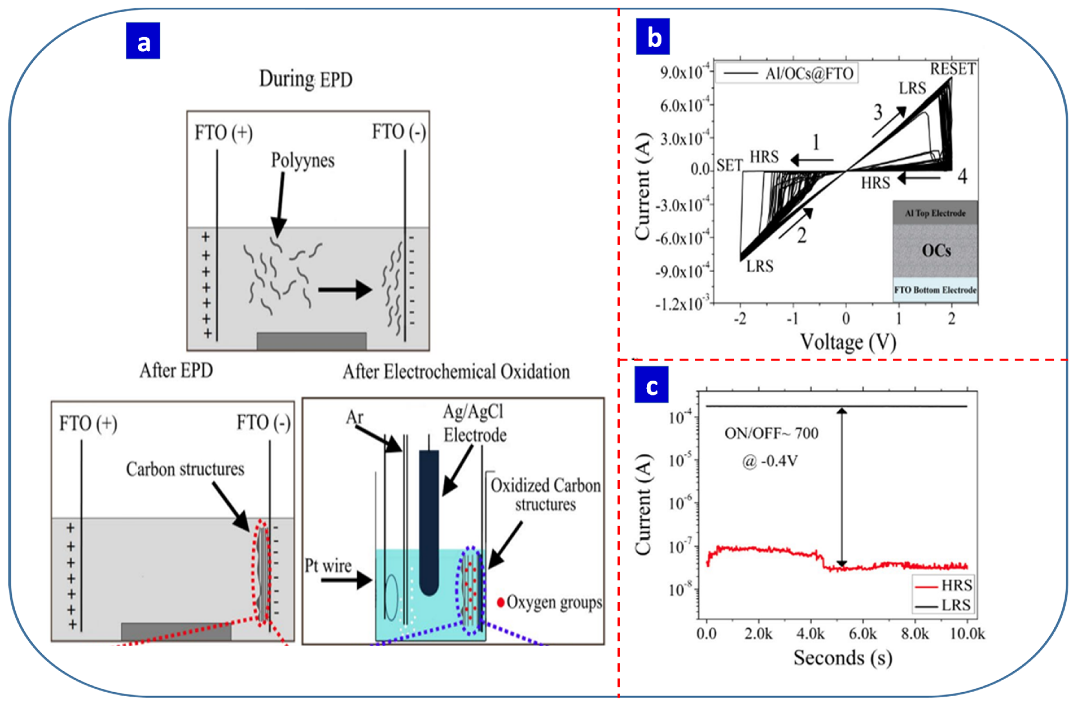
6.1. Carbon-Based Resistive Switching Devices

There are very few reports available on carbon-based RS devices [137]. In recent years, graphene oxide [138,139], diamond-like carbon [140], carbon quantum dots [141], single-walled carbon nanotube (SWCNT)@TiO2 core–shell wires [142], graphene oxide-TiO2 [143], self-generated amorphous carbon [144], graphene-integrated devices [145], and carbon nanotubes have been explored for use in RS memory applications [146], but very few of these have been electrochemically synthesized. Carbon materials have numerous advantageous properties related to their morphology, defects, percentage of oxygen groups, and sp2 and sp3 carbon atoms, and these properties can be utilized to tune the RS effect of a device [35,137].
Russo et al. reported a new electrochemically deposited carbon material for RS devices with free bipolar RS properties [35]. They generated carbon nanowalls (CNWs) via electrophoretic deposition from arc-discharged polyyne electrolytes and demonstrated that the defects in and the orientation of the CNWs affected their electrical resistivity, with the presence of oxygen vacancies and a perpendicular orientation leading to an LRS in an Al/CNW/FTO device. Additionally, trapping and de-trapping electrons in oxygen vacancies with a positive and negative bias switches the device between an LRS and an HRS, respectively [35]. In 2019, Russo et al. reported the electrophoretic deposition of carbon material for memory application [137]. They employed a two-step synthesis approach that combined the electrophoretic deposition of the carbon material with subsequent electrochemical oxidation to produce an active switching layer (Figure 6a) [137]. They reported that the content of oxygen and carbonyl groups (C=O) in the electrochemically oxidized carbon material controlled the RS properties. The anodically oxidized carbon material exhibited three-level memory behavior and a higher ON/OFF ratio than non-oxidized carbon materials. Figure 6b,c present the cyclic stability and retention of the Al/oxidized carbon structures@FTO device [137], with the degree of oxidation well controlled by the anodic oxidation parameters. The oxidized carbon material exhibited RS behavior within a ±2 V range. While a higher percentage of carbonyl groups (C=O) did not provide a higher ON/OFF ratio, the amount of sp3 and sp2 carbon atoms and oxygen-containing carbon groups did play a key role in the Al/OC@FTO device [137]. Liu and co-workers also reported that the electrophoretic deposition of graphene oxide could potentially be used in memristive devices [147]. This is because the oxygenation levels of graphene oxide can affect the properties that are tuned using electrophoretic parameters. Their fabricated Al/GO/ITO device had an ON/OFF ratio of more than 10 and a retention time of 100 s [147]. Table 3 summarizes the electrochemically prepared carbon-based materials for memory applications. This summary highlights a considerable research gap in terms of electrochemically synthesized carbon materials for RS-based memory devices.

6.2. ZnO-Based Resistive Switching Devices

In recent years, transition metal oxides have attracted significant attraction due to their CMOS compatibility and ease of synthesis [148]. ZnO is the most common metal oxide used in electrochemical synthesis. As with carbon materials, the orientation and morphology of ZnO can affect the RS properties. Jing et al. synthesized ZnO-based RS devices, and Figure 7a presents the structure of their electrodeposited ZnO thin-film-based device [36]. They produced nanoflake, agglomerated nanoparticle, and nanorod morphologies by tuning the deposition temperature and found that the Au/ZnO nanorod/FTO device had strong RS properties, while the ZnO nanoflakes and nanoparticles did not (Figure 7b). The ZnO nanorod-based device exhibited an endurance of 2000 cycles and retained data for up to 1800 s (Figure 7c,d, respectively) [36]. In another study, Yusoff et al. synthesized ZnO nanowires using two-step electrodeposition and thermal oxidation. They varied the deposition time to investigate the effect of the nanowire size, the thickness of the film, and the RS properties of the device [149].
A cyclic voltammetric deposition is an essential form of electrochemical deposition. In this technique, an applied voltage is swept between specific voltage ranges, producing a thin film with superior surface coverage compared with conventional electrodeposition [104]. Sun et al. fabricated a Au/ZnO/AZO structure in which ZnO thin film was cathodically electrodeposited in a zinc nitrate solution [150]. The electrochemical deposition was carried out potentiostatically in a conventional three-electrode cell at −0.9 V with a constant temperature of 353 K and a deposition time of 1000 s. The RS properties were tuned by simply adding nitric acid to the electrolyte. They reported that the reaction of nitric acid with OH- ions in the electrolyte decreased oxygen availability, leading to more oxygen vacancies and n-type conductivity in ZnO. The ON/OFF ratio significantly decreased with an increase in the nitric acid concentration. A low concentration of nitric acid led to few oxygen vacancies while a high concentration did not induce the RS effect. When the carrier concentration was higher than 1019 cm–3, the materials did not exhibit any RS properties [150].
Fuzi et al. also fabricated a flexible Au/ZnO/ITO/PET RS device using electrodeposition. They reported that deposition time is an essential parameter when tuning the RS properties [148]. Figure 7e presents the semi-logarithmic I–V curves for electrochemically prepared ZnO thin films deposited for 15, 30, 60, and 120 s. Above 60 s, the device did not exhibit any notable I–V characteristics, while the ROFF/RON ratio decreased with increasing deposition time (Figure 7f). The combination of electrochemical with other techniques assisted in the oxidization of Zn, leading to stronger RS properties than electrochemically deposited ZnO. In particular, thermal oxidation is commonly used in conjunction with electrochemical synthesis. For example, Quintana et al. synthesized faceted and spongy single-crystal ZnO using a combination of electrodeposition and hydrothermal techniques [151]. The faceted and spongy Zn rods were synthesized galvanostatically and potentiostatically, respectively, followed by hydrothermal treatment in distilled water to produce ZnO rods. The end device exhibited good I–V and retention properties.
Many research groups have synthesized composite, doped, bilayer, and decorated semiconductor materials to improve RS properties. Recently, Younis et al. synthesized a Ti-doped ZnO thin film from Zn(NO3)2·6H2O via electrodeposition on ITO [152]. The Au/Ti@-ZnO/ITO device exhibited electroforming-free and current compliance-free memory effects and typical bipolar RS properties with good SET (2.9 V) and RESET (−2.7 V) voltages. The device was stable for up to 200 cycles and retained data for up to 2000 s. The memory margin of the device with a 2% Ti@ZnO structure was much higher than that of the control device (pure ZnO) [152].
Bilayered and trilayer devices have also been shown to have tunable RS properties. For example, Fauzi et al. electrodeposited ZnO on a copper substrate followed by thermal oxidation to produce a Au/ZnO-Cu2O-CuO/Cu RS device. Figure 8a,b present the electrodeposition setup and device structure, respectively [153]. A trilayer structure was observed due to thermal oxidation. The active layer thickness (ZnO-Cu2O-CuO) was approximately 81 nm. The authors reported that the HRS/LRS ratio was directly proportional to the thickness of the thin film (Figure 8c,d); as the thickness increased with longer deposition times, the difference between the resistance of the LRS and HRS and the HRS/LRS ratio tended to decrease. In 2018, Fauzi et al. deposited Ti and Zn on a Cu substrate using dilute electrodeposition and subsequently oxidized it thermally at 600 °C. They observed that the Au/TiO2-Cu2O-CuO/Cu device had a higher HRS/LRS difference than Au/ZnO-Cu2O-CuO/Cu. They suggested that metal ion formation was responsible for the RS effect in their device [154].
The decoration of ZnO with quantum dots can also enhance RS properties. Younis et al. electrochemically synthesized ZnO nanorods decorated with CeO2 quantum dots (∼5 nm; Figure 8e) [155]. The average diameter and length of the ZnO nanorods were ∼20 and ∼200 nm, respectively. The fabricated Au/CeO2−ZnO/FTO device exhibited stronger memristive properties than the Au/ZnO/FTO device (Figure 8f). In terms of the temperature dependence of the RS characteristics, the CeO2−ZnO nanocomposite showed no change in the memory window. However, the memory window of the ZnO nanorod-based device tended to decrease as the temperature increased. Figure 8g,h depict the endurance and retention properties of the Au/CeO2−ZnO/FTO device. Their results suggested that the decoration of CeO2 quantum dots improves the RS characteristics of electrochemically synthesized ZnO nanorods [155]. The electrochemical approach is also useful for tuning the charge transport within a device. Ocampo et al. fabricated nanostructured porous Si-metal-oxide (ZnO and VO2) composites, with the porous Si-ZnO device exhibiting better memristive properties than the Si-VO2-based RS device due to the higher porosity of the ZnO, which facilitated charge transport within the active switching layer [156].
Table 4 summarizes the electrochemically synthesized ZnO-based RS devices that have been reported to date. The electrodeposition technique has frequently been used for material synthesis, but further research is warranted on the synthesis of anodization-based ZnO RS materials. It is important to note that electrodeposited ZnO RS devices require higher switching voltages than physically deposited RS devices, while their memory window, endurance, and retention properties are also lower. Given this, research should focus on improving the non-volatile memory performance of electrochemically synthesized ZnO RS devices.

6.3. TiO2-Based Resistive Switching Devices

Memory storage devices based on transition metal oxides have been well studied in recent years. In particular, TiO2 has been the most widely researched material for RS memory applications. In 2010, Miller et al. synthesized titanium dioxide using anodization for memory storage applications and investigated the memristive properties of both annealed and nonannealed devices. The nonannealed anodized TiO2 exhibited a pinched hysteresis loop, while the annealed films did not demonstrate any significant RS properties. There is no need for the post-deposition annealing of anodized films due to the inherent presence of oxygen vacancies at the Ti/TiO2 interface [37]. There have been very few reports available on the fabrication of TiO2 nanotubes using electrodeposition for memristor applications, but it is clear that electrodeposition can produce TiO2 nanotubes for RS applications [157]. Power consumption is an important aspect of RS devices that depends on the operating voltage. Therefore, there is a need to fabricate devices with a lower switching voltage. In this respect, anodically prepared Au/TiO2/Ti devices can be operated within ±0.3 V [158].
The anodization of Ti foil in different electrolytes leads to the formation of TiO2 nanotubes with different shapes, leading to devices with different RS properties. For example, Nirmal et al. synthesized highly ordered TiO2 nanotubes via the anodization of Ti foil, with the proposed growth mechanisms presented in Figure 9a. They deposited Al as the top electrode via sputtering, and the resulting Al/TiO2/Ti device (Figure 9b) exhibited RS within ±2 V (Figure 9c). The endurance and retention of the fabricated device are displayed in Figure 9d,e, respectively. They proposed a filamentary-type RS model (Figure 9f) and mimicked different STDP rules utilizing the analog behavior of the proposed memristive device (Figure 9g,h) [133]. Similarly, Yoo et al. synthesized highly ordered TiO2 nanotubes via the anodization of Ti foil in an HF/H3PO4 electrolyte. The TiO2 nanotubes had a V-shaped morphology and a short aspect ratio, which was suitable for Pt coverage. The Pt/TiO2/Ti device exhibited RS within ±1 V [159].
Similarly, Yin et al. fabricated a Pt/TiO2/Ti device in which TiO2 was deposited via anodization in an H2SO4 electrolyte. Interestingly, four stable resistance states were observed in the prepared device. The eightwise and counter-eightwise I–V curves indicated the coexistence of ion- and electron-dominated RS mechanisms [160]. The choice of the top electrode in an anodic TiO2-based RS device influences its RS properties. Given this, Yu et al. reported an anodic TiO2-based RS device with Ag and Au as the top electrodes. The Au-based device did not exhibit any notable I–V characteristics; however, with the Ag top electrode, improved I–V characteristics were observed. They also reported that anodizing for only 5 min produced a TiO2 device with more suitable properties than the anodization times of 1, 3, and 10 min. Thus, the deposition time is also a very sensitive parameter for electrochemically synthesized RS devices [161].
Tao et al. fabricated a Cu/TiO2/Ti nanopore array membrane device using two-step anodization [162]. First, Ti foil was anodized in an NH4F-based ethylene glycol electrolyte and washed in an ultrasonicator. It was then anodized in the same electrolyte under an ice bath at 20 V, 40 V, and 60 V. The devices anodized at 20 V and 40 V did not require electroforming steps. RS occurred within a ±1 V window, and the RHRS/RLRS ratio increased as the anodization voltage increased. Generally, electrochemical metallization was observed in the device with a Cu top electrode, but the Cu/TiO2/Ti device exhibited Ohmic conduction. This suggested that the oxygen vacancies led to the formation of conduction filaments in the TiO2 during the SET process. The device was composed of Cu nanocones and Ti nanopores, with a highly concentrated electric field between the two, which enabled the migration of oxygen vacancies [162]. Chen et al. also fabricated core–shell copper nanowire-TiO2 nanotubes (TNTs) via anodization and electrodeposition [163]. The TNTs were synthesized using two-step anodization, while the Cu nanowires were grown on the TNTs using electrodeposition. The RS properties were investigated for both Au/TNTAs/Ti and Au/Cu nanowire-TNTAs/Ti devices, with the Cu nanowire-TNTA-based device exhibiting both analog and digital RS properties. The device was stable for 104 cycles and was able to retain data for 104 s [163].
Table 5 summarizes the previously reported electrochemically prepared TiO2-based RS devices [37,157,158,159,160,161,162,163,164,165,166]. Unlike ZnO, anodization was frequently used for the synthesis of TiO2 for RS memory applications. All of the electrochemically prepared TiO2 RS devices have demonstrated suitable switching voltages. However, improvements in the memory window, endurance, and retention properties of electrochemically prepared TiO2 RS devices are required.

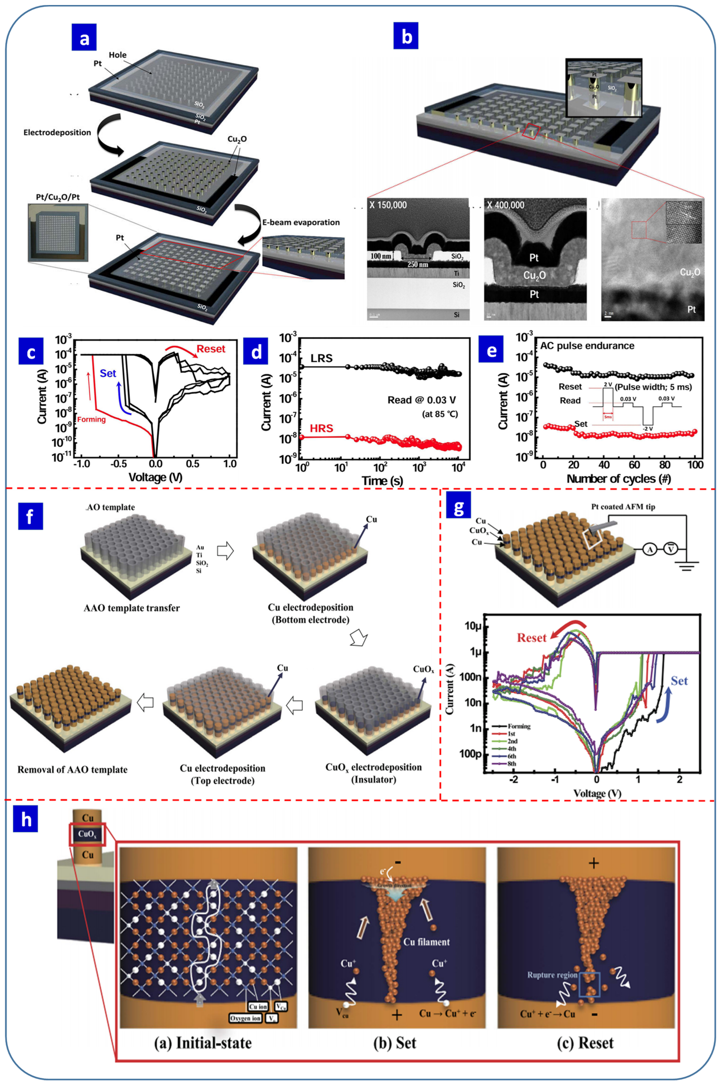
6.4. Cu2O-Based Resistive Switching Devices

Cu2O has been frequently employed for various applications, including memory [167,168,169], photocatalysis [170], solar cells [171], supercapacitors [172], and gas sensing [173]. However, Cu2O has not been well explored for RS applications. Cu2O has the potential to be compatible with integrated circuit fabrication processes. Yazdanparast et al. reported unipolar RS properties for electrodeposited Cu2O on a Au-coated glass substrate in a highly alkaline tartrate bath. The RS of their device was attributed to the formation and rupture of Cu filaments, with an initial resistance of 6.5 × 10⁶ Ω. The LRS of the device demonstrated a linear decrease in resistance with decreasing temperature, suggesting the formation of Cu filaments. The calculated diameter (70 nm) and resistance temperature coefficient (1.57 × 10⁻³ K−1) in an LRS confirmed the formation of Cu filaments, which were nearly equal to Cu nanowires. The authors also calculated the temperature (798 ± 55 K) of the Cu filaments during the RESET process, which caused the rupture of the filaments due to Joule heating [174]. In another study, the same research group reported the effect of various electrodeposited parameters on RS properties. Electrodeposition voltage can be used to tune the size of the electrodeposited microstructure and RS properties, and their study found that decreasing the applied negative voltage increased the grain size of Cu2O. Additionally, the grain size increased with an increase in temperature. They observed that the forming voltage decreased with an increase in the electrodeposited negative potential and an increase in temperature. Furthermore, the SET/RESET voltage was dependent on the grain size of the material. In addition, the LRS current did not depend on the grain size or the surface area of the top electrode, which suggested that filamentary conduction is the dominant mechanism in Au/Cu2O/Au-Pd devices [175].
Fabrication of high-density memory storage devices is a major challenge that can be achieved by scaling down the size of the device and developing cross-point array structures, which require precise, large-scale, and selective area deposition methods. In this respect, electrochemical deposition can be used to precisely fabricate active switching layers. Recently, Han et al. fabricated a memory device by electrodepositing Cu2O (70 nm) within the holes of a SiO2 substrate on a Pt bottom electrode. The top Pt electrode was deposited using an e-beam evaporator (Figure 10a) [167]. The size of the cell is presented in Figure 10b [167]. The device exhibited bipolar RS within ±1 V and a forming voltage within ±1 V, representing a low power consumption (Figure 10c) [167]. The fabricated device also demonstrated good retention (Figure 10d) and endurance (Figure 10e) [167]. In another study, the same research group fabricated Cu/CuOx/Cu devices using the electrodeposition of Cu, CuOx, and Cu on an AAO template (Figure 10f) [168]. The active layer thickness and pore diameter of the AAO template influenced the SET/RESET voltage of the devices. The device structure and I–V characteristics of the electrochemically deposited Cu/CuOx/Cu devices are presented in Figure 10g [168]. The RS mechanisms of these devices depended on the top and bottom electrode material because the ionization energy of Cu is lower than that of Cu2O. The authors suggested that, when a positive bias was applied to the bottom electrode, the Cu induced the diffusion of Cu+ ions into the Cu2O layer. Furthermore, the Cu ions drifted from the top electrode to the bottom electrode and formed Cu conduction filaments in the switching layer. The filaments were ruptured by applying a negative bias to the bottom Cu electrode (Figure 10h) [168]. Patil et al. also fabricated Al/Cu2O/FTO memristive devices based on an electrochemical approach, showing that the space charge-limited current (SCLC) mechanism was responsible for conduction, while RS occurred due to the filamentary effect [176].
Flexible memory storage devices are the future of ubiquitous computing systems. To fabricate a flexible memory device, a flexible substrate is employed to support the entire device. Recently, Park et al. electrodeposited Ni/CuOx/Ni on a flexible polyethylene terephthalate (PET) substrate, producing a device with reliable RS and endurance. The fabricated device exhibited strong performance under flat, tensile, and compression stress [177]. Kim et al. also fabricated a self-compliance-based bilayered memory device with a Pt/CuOx/CuOx/Pt structure. The electrical properties of the CuOx layers were tuned by controlling the pH of the electrolyte. In their device, one CuOx layer acted as an internal resistor while the other operated as an RS layer. Due to the internal resistor, the LRS current was controlled and reproducible RS properties were observed without current compliance [178]. Electrochemical approaches can also be extended to the fabrication of metal sulfide-based RS devices. For example, Yan and co-workers fabricated Ag/Cu2S/Ag and Ag/Cu2S/Cu memristive devices and recorded good RS performance [179].
Table 6 presents previously reported electrochemically synthesized Cu2O-based RS devices. The RS performance of these devices is not yet satisfactory. More attention should be focused on improving their memory window, endurance, and retention properties. Furthermore, electrodeposition has frequently been employed to synthesize Cu2O-based RS devices; thus, other electrochemical approaches should be researched to achieve high-performance RS memory devices. The choice of the electrolyte in electrochemical synthesis affects the morphology and composition of the active layer material, which impacts the RS properties of the end device. For Cu2O-based RS devices, CuSO4-based electrolytes have been preferred in combination with acid and NaOH. Lactic acid, sulfuric acid, and tartaric acid have been the most preferred choices of researchers for the electrochemical synthesis of Cu2O-based RS devices. Therefore, RS properties could be improved further by testing other electrolytes during the synthesis of Cu2O.

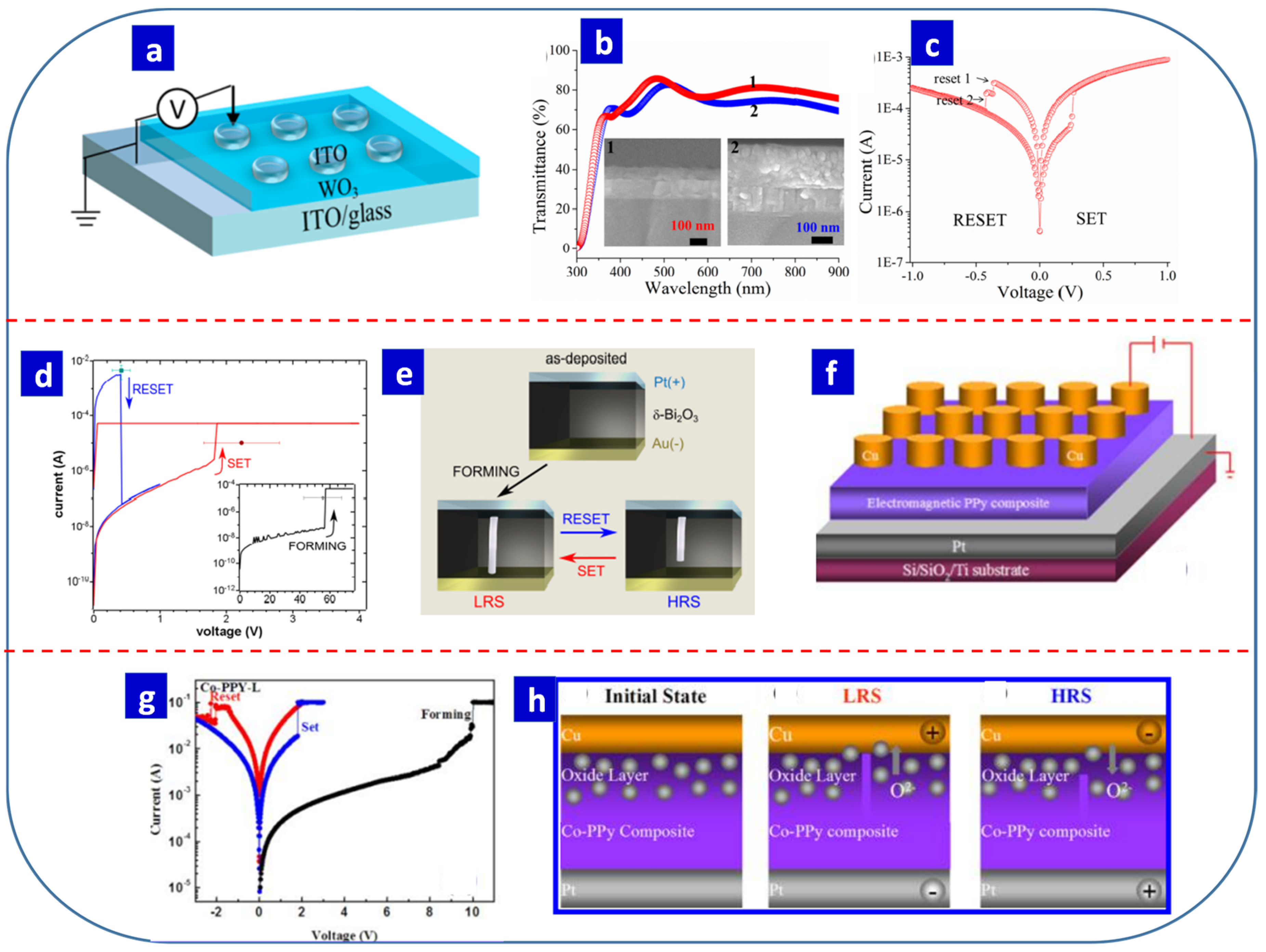
6.5. Other Metal-Oxide- and Composite-Based Resistive Switching Devices

Transition metal oxides are promising switching layer options for RS devices. Electrochemically synthesized ZnO, TiO2, and CuO are transition metal oxides that are frequently used for RS memory applications, while NiO, MnO2, WO3, Ta2O5, ZrO2, and Co3O4 have also been reported for RS memory applications [180,181,182,183,184,185]. Nanotemplate-based synthesis has recently been reported to be a promising technique for RS devices. Recently, Kim et al. reported NiO nanowire-based devices fabricated via electrodeposition with AAO membranes. The fabricated device exhibited similar RS properties to those of NiO thin films. The authors reported that the operating voltage of the device was directly proportional to the length of the NiO nanowires [186]. In the same vein, Song et al. fabricated AAO nanotemplates based on Ni/NiO/Ni devices with cell sizes of less than 100 nm. They were able to produce NiO nanodots with a high density (1 × 10¹⁰/cm2) and uniformity. The fabricated device exhibited unipolar RS characteristics. Interestingly, NiO doping with phosphorous switched the Au/NiO/Au device from unipolar to bipolar when fabricated using AAO template-based electrodeposition. The fabricated device operated within ±1 V [187]. AAO nanotemplate-based nanopatterning techniques thus have significant potential for use in high-density memory applications [88].
Valve metal oxides and valve metal alloy oxides can also be tailored electrochemically to boost the performance of RS devices. Sophocleous et al. demonstrated a TaOx-based device with good memristive properties. A switching layer with a thickness of 10 nm was fabricated using electrochemical anodization, and a high ON/OFF ratio was obtained. The device was low-cost and environmentally friendly and exhibited better RS performance with possible CMOS compatibility [188]. Zaffora et al. also reported a Ta/Ta2O5/Pt-based RS device with the active switching layer fabricated using anodization in a borate buffer electrolyte. The device had a stable LRS and HRS for up to 106 cycles and a retention of up to 104 s. The SET and RESET times for the device were 20 ns and 165 ns, respectively [189]. In 2019, the same research group fabricated a device based on the anodization of Ta and an Al alloy for RS applications. The device had similar properties to an anodic Ta2O5-based RS device. They also fabricated a mixed Hf-Nb oxide via the anodization of Hf and Nb. Their results suggested that this electrochemical approach has significant potential for the production of high-quality thin films for RS devices [132].
Flexibility and transparency can expand the range of applications for RS devices. Interestingly, WO3-based RS devices have been reported to show both characteristics. Ji et al. fabricated a Cu/WO3−x/ITO-based flexible RS device using anodization. The device had a high ION/IOFF ratio of ~105 and a stable retention of up to 5 × 10⁵ s. They also reported outstanding uniformity over 103 bending cycles [190]. Qian et al. fabricated a highly transparent ITO/WO3/ITO RS device using cathodic electrodeposition (Figure 11a) [180]. The device had high optical transmittance (Figure 11b), a low operating voltage (Figure 11c), and a long retention time (>104 s) [180]. Electrochemically deposited Mn3O4 devices can also exhibit RS characteristics. Koza et al. deposited Mn3O4 potentiostatically in an acetate electrolyte with a potential range of 0.20–0.35 V. The Mn3O4 thin film has unipolar RS properties, and the SET and RESET times of the device were 2 and 50 ns, respectively [43]. An electrodeposited δ-Bi2O3-based RS device has also been reported to be unipolar (Figure 11d) [181]. The authors concluded that the formation and rupture of Bi filaments were responsible for switching in a Pt/δ-Bi2O3/Au memory cell (Figure 11e) [181]. Recently, electrodeposited VO2 has also been reported for RS applications [191,192]. An electrodeposited P-type CO3O4 nanosheet-based device exhibited bipolar RS behavior and a stable RS process over 200 cycles, with data retained for up to 104 s. [193]. Oxidized MoS2 is also an attractive material for RS applications due to its promising memristive properties. Jamilpanah et al. reported an electrodeposited MoS2-MoO2-MoO3-based RS device with ECM and VCM mechanisms when using Ag and Au top electrodes, respectively. Interestingly, the annealing of the composite created pure-phase MoS2 and MoO3 in Ar and air, respectively, which did not demonstrate memristive properties [194].
As with programmable solid-state metallization cells, liquid-state metallization cells produce good results in aqueous systems. Han et al. fabricated a device by stabilizing the aqueous growth of Cu in polycarbonate nanopores with the use of shock electrodeposition. The device exhibited considerable I–V characteristics and endurance for up to 500 cycles with a retention time of <10 s [195]. Polymer-based composites can also exhibit useful RS properties. For example, Xu et al. fabricated a Co-nanoparticle dispersed polypyrrole (PPy) based on an electrochemical approach for RRAM applications (Figure 11f) [182]. Metal nanoparticles were composited with a polymer, which enhanced the spontaneous oxidation of the conducting polymer. The RS mechanism of the device was based on oxygen ion mobility, which was able to be tuned by the metal nanoparticle concentration. The Cu/Co−PPy composite/Pt device exhibited stable bipolar RS (Figure 11g), which was due to oxygen ion movement within the switching layer (Figure 11h) [182]. Electrodeposited Prussian blue [196], AAO template-based electrodeposited Bi1−xSbx [197], and electrodeposited copper tetracyanoquinodimethan [198] have also been reported for RS memory applications.
Table 7 summarizes the electrochemically fabricated metal oxides, composites, and polymer-based RS devices reported to date. There is a broad scope for synthesizing oxide- and polymer-based RS materials using electrochemical approaches, leading to greater RS memory performance than existing devices. Many important properties such as surface area, power consumption, switching uniformity, and reliability need to be investigated further to fabricate high-performance memory devices. Importantly, flexible and physically transient switching layers have rarely been synthesized using electrochemical approaches. In the future, these devices will play an essential role in many applications.

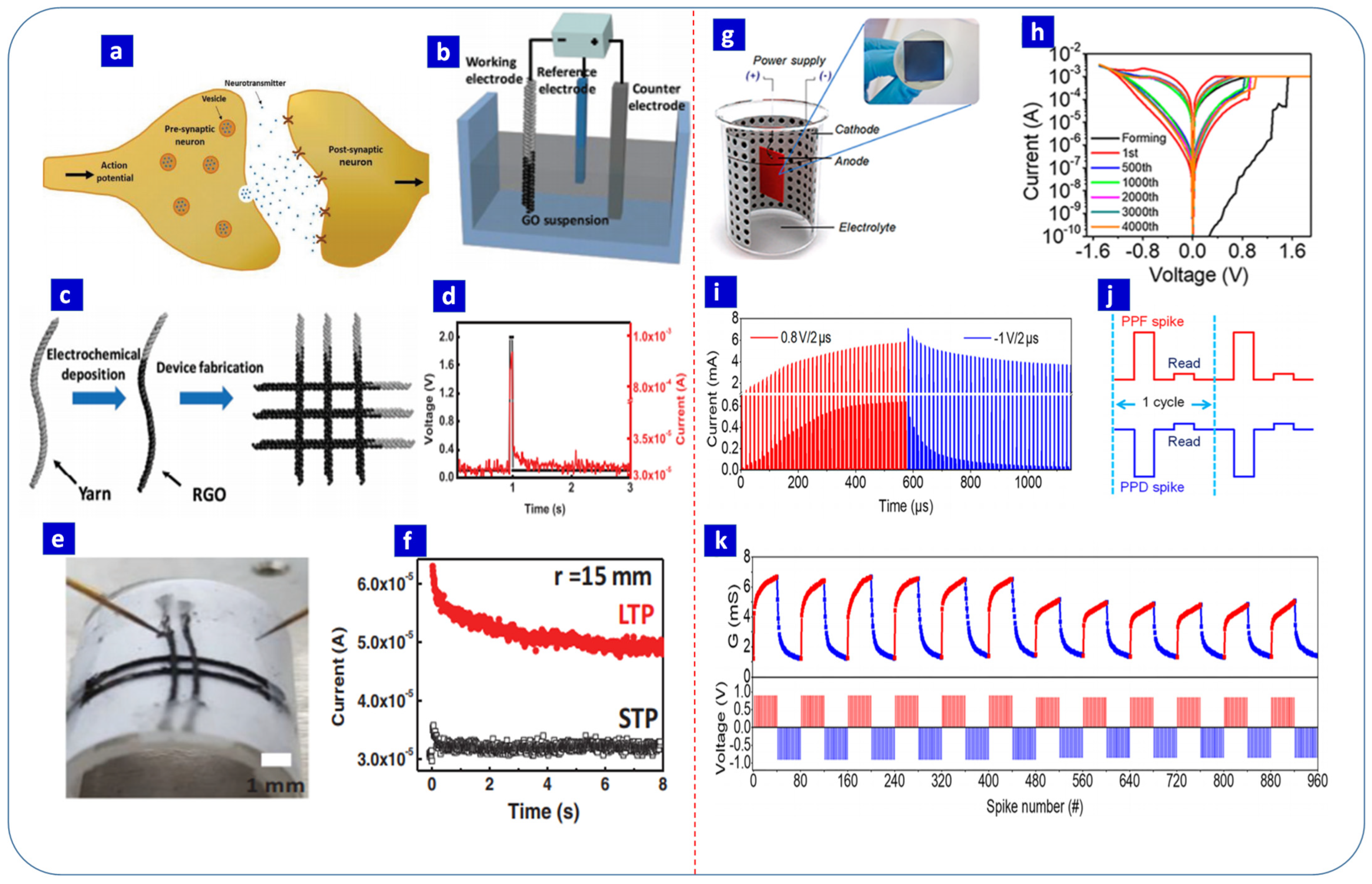
7. Electrochemically Synthesized Resistive Switching Materials for Neuromorphic Computing Applications

In neuromorphic computing applications, electronic devices generally mimic biological synaptic properties. In biological synapses, the pre-neuron transfers an electrical/chemical signal to the post-neuron via the synaptic cleft and modulates the signal amplitude and shape of the post-synaptic spike. This process involves different biological mechanisms and is referred to as synaptic learning [199,200,201,202,203,204]. Figure 12a presents a typical biological synapse of the human brain [205]. Due to structural and mechanistic similarities, RS devices are generally used to mimic bio-synaptic properties. Artificial or electronic synaptic devices can mimic some synaptic rules and properties, including STDP, SRDP, potentiation, and depression [1]. Several electronic devices can operate as artificial synaptic devices, such as RS/memristors [92], transistors [93], and ferroelectric junctions [94]. Of these, RS/memristor devices are the most suitable candidates due to their tunable electrical properties.
Electrochemically synthesized devices can also be employed as artificial synaptic devices, but limited research has been conducted in this area. In particular, electrochemically prepared metal oxides, chalcogenides, and polymers can mimic bio-synaptic properties. Recently, Park et al. reported electrochemically synthesized reduced graphene oxide (rGO) as a wearable textile for neuromorphic applications. They electrodeposited rGO on stainless conductive yarns following the electrochemical reduction of GO (Figure 12b,c) [205]. The fabricated device exhibited an excitatory post-synaptic current (EPSC) and paired-pulse facilitation (PPF) (Figure 12d). By controlling the amplitude of the applied pulse, the device could switch from STP to LTP. The device also exhibited stable neuromorphic properties under bending (Figure 12e,f), highlighting its suitability for integrated textile applications [205].
An anodic oxide is a promising option for neuromorphic applications, but only two reports of electrochemically fabricated devices containing this material are available in the literature. Chen et al. reported Pt/TiO2−x/Ti-based electronic synapse devices with a switching layer that was fabricated via anodization of a Ti substrate [206]. The electrochemical setup for anodization is depicted in Figure 12g, with the fabricated device exhibiting RS for up to 4500 switching cycles (Figure 12h). A rapid switching time (90 s) and multistate conductance were also observed for this device. PPF, paired-pulse depression, and the applied pulse waveform are presented in Figure 12i,j. The device also mimicked the potentiation and depression properties of biological synapses (Figure 12k). Choi et al. also fabricated a Pt/TaOy/nanoporous TaOx/Ta crossbar array structure via the anodization of the Ta layer in an aqueous sulfuric acid electrolyte [207]. The fabricated crossbar array structure minimized the undesired leakage current through neighboring cells. The device exhibited high non-linearity (104), low synapse coupling (4.00 × 10⁻⁵), and good endurance and retention. The authors also mimicked basic and advanced synaptic properties such as LTP, LTD, and STDP. They reported that the device had an 89.08% recognition accuracy after 15 training epochs. As discussed earlier, very few reports are available in the literature related to electrochemically synthesized artificial synaptic devices; thus, they require further investigation. Table 8 summarizes the synaptic learning properties of electrochemically fabricated RS devices for neuromorphic computing applications.

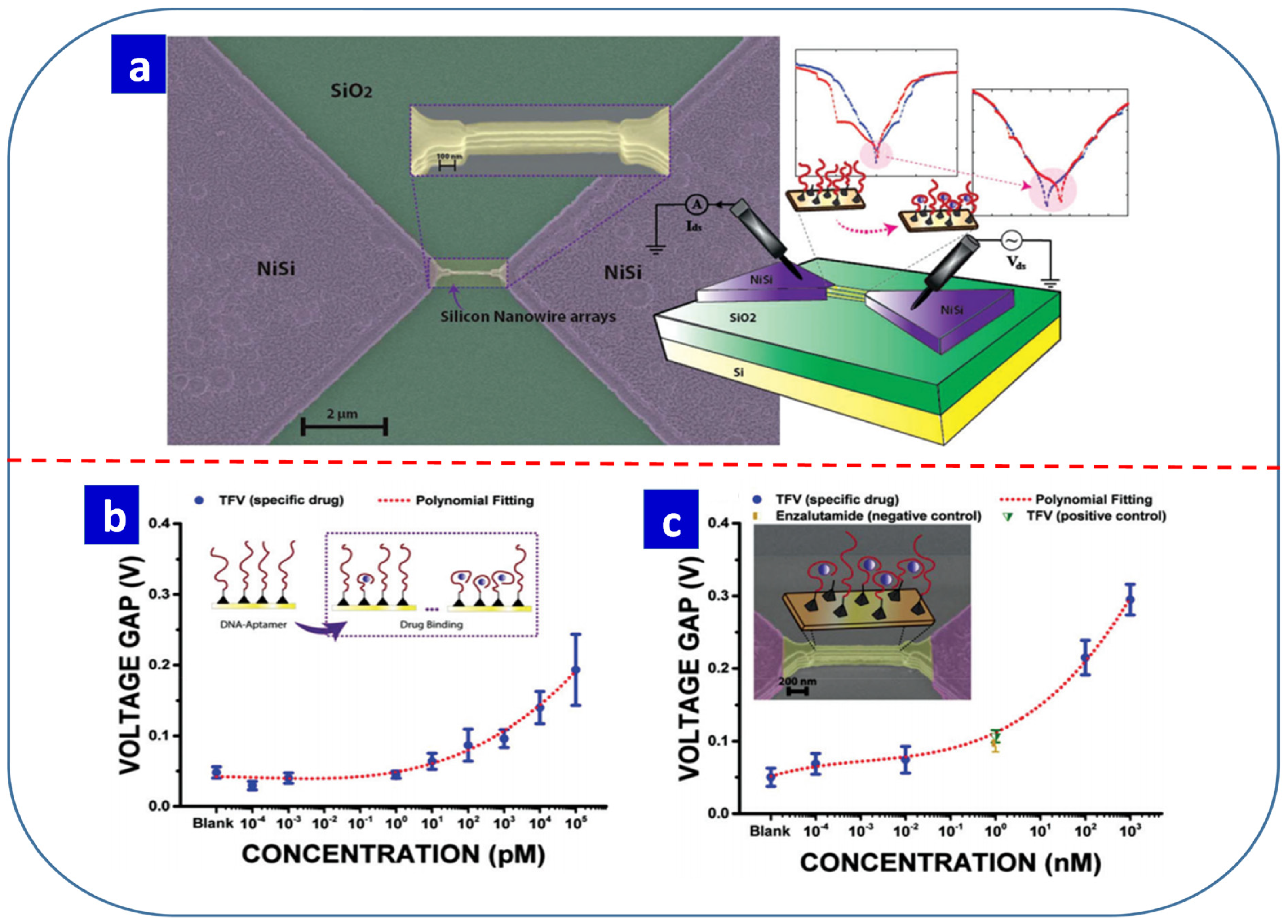
8. Electrochemically Synthesized Resistive Switching Materials for Sensing Applications

Due to rapid industrialization, pollution has emerged as a major global challenge. Therefore, there is a need to identify specific pollutants and physical and biological entities in drinking water, food, and the air before they can harm human health, while bio-sensors are needed for the early diagnosis of health issues. In this context, several sensor technologies have been investigated to reduce costs, increase portability and sensitivity, and improve recycling capabilities. In particular, in recent years, many researchers have looked to fabricate sensors that utilize the RS effect, including those for the detection of ascorbic acid [75], drug levels [49], glucose/saliva [208], heavy metals [209,210], gas [211,212], and radiation [213]. For example, Figure 13a presents a memristive aptasensor that can sense drugs based on RS [49]. The change in electrical characteristics such as the voltage gap is a response to the change in the drug concentration and human serum (Figure 13b,c) [49]. Based on this, the drugs are analyzed both quantitatively and qualitatively.
To the best of our knowledge, there have been no reports of electrochemically prepared RS materials being used for sensing applications, but the working principle of many sensors is based on electrochemical sensing. For example, a pH sensor has been developed that utilizes the RS effect at the electrolyte–oxide–semiconductor interface [214]. The device was fabricated with Pt as the bottom electrode and SiO2 as the switching layer. For electrochemical characterization, Pt was employed as the counter electrode and Ag/AgCl as the reference electrode. The authors reported that the threshold voltage of the device increased linearly with an increase in the pH from 1 to 12 with high linear sensitivity (46.3 mV/pH). The contact between the electrolyte and SiO2 layer formed an electric double layer that led to the aggregation of ions at the interface. Under forward bias, positive ions were injected into the SiO2 layer to form conduction filaments, and the device switched to an LRS. Under a reverse bias, the device switched to an HRS by extracting the ions from the SiO2 layer. The change in the concentration of positive ions in an electrolyte changes the RS properties, allowing the pH of the electrolyte to be determined [214]. Overall, electrochemically prepared materials have been employed in many sensing applications. Combining the advantages of these materials with RS holds promise for the development of novel sensor designs.

9. Future Outlook

The present literature review has shown that the electrochemical synthesis of RS devices can reliably produce high-performance memory, synaptic, and sensor devices. However, electrochemical synthesis has not been fully explored compared to other solution-processable and physical deposition techniques. Very few electrochemically fabricated devices are available, and various synthesis techniques, nano/micromaterials, and device structures need to be tested to maximize the potential of this area of research. The effects of electrochemical parameters on RS properties have also not been well explored in past studies. Therefore, future research on various electrochemically synthesized materials and corresponding engineered devices is required in the form of well-planned experiments to realize high-performance RS devices for use in memory, neuromorphic computing, sensor, and security applications.
Most previous research has employed electrochemical techniques only for the fabrication of switching layers, while standard physical deposition techniques are used for the top and bottom electrodes. However, it is possible to synthesize an entire RS device using electrochemical fabrication, which would help to reduce production costs and simplify the fabrication process. One such device has already been reported by Han et al., utilizing a bottom-up approach [168]. Working on similar lines, all-electrochemically fabricated RS devices could revolutionize non-volatile memory and neuromorphic computing. In particular, electrochemically synthesized carbon nanomaterials have significant potential for use in various fields, particularly due to their strong RS behavior. One of the advantages of electrochemical synthesis is that it allows for the uniform deposition of carbon materials on conducting substrates; thus, graphene [215], graphene oxide [216], and CNTs [217] can be used as an active switching layer and top/bottom electrodes in RS devices via electrophoretic deposition or electrodeposition. While ZnO, TiO2, and CuO are the most commonly electrochemically synthesized materials for RS applications, the electrochemical approach also supports the synthesis of CMOS-compatible materials such as HfO2, TaOx, and Ta2O5. Therefore, it is recommended to synthesize these materials using a variety of electrochemical synthesis techniques.
Tuning the electrochemical parameters (such as the electrolyte precursor, electrolyte concentration, pH, deposition time, and deposition temperature) can also be used to enhance RS properties. Moreover, the morphology and/or orientation of the material can be adjusted to influence the RS properties and mechanisms [35]. Doping, metal decoration, composites, and bilayered structures have proved effective in this respect for various applications. In particular, it has been demonstrated that the decoration of metal oxides with metal [218], the use of core–shell structures [219], and the fabrication of bilayered structures can improve the RS properties of a device. Multilayered electrodeposited devices can also exhibit stronger RS properties. In addition to metal oxides, polymers [220] and metal–organic materials [221] can be deposited using electrochemical synthesis and are suitable for neuromorphic and sensing applications. However, few studies reported on electrochemically synthesized polymer-based RS devices. Therefore, further exploration of electropolymerization is recommended, as this technique has the potential to achieve impressive RS properties. In addition, PCM is an emerging RS device, and its electrochemical fabrication may pave the way for the future development of RS applications. Most commonly employed phase-change memory materials (i.e., Ge-Sb-Te) can be electrochemically deposited onto a conducting substrate in a nonaqueous electrolyte using a three-electrode system (conducting substrate: working electrode, Ag/AgCl: reference electrode, and Pt: counter electrode). Recently, Huang et al. developed GeSbTe phase-change memory cells using a non-aqueous electrodeposition technique [69]. Here, an electrolyte contained [NBun4][GeCl5], [NBun4][SbCl4]s, and [NBun4]2[TeCl6]. [NBun4]Cl was added to the CH2Cl2 as a supporting electrolyte, with Ge-Sb-Te ultimately electrodeposited at −1.75 V vs. Ag/AgCl. Similar to this approach, binary and ternary chalcogenides can be deposited on conductive substrates for RS applications. In addition, given that most top and bottom electrodes are either metal or conducting materials, it is possible to exploit electrodeposition to fabricate and/or pattern top and bottom electrodes. Considering the previously identified research gaps in the literature, we believe that the electrochemical approach holds significant promise for the fabrication of state-of-the-art RS devices.

10. Conclusions

This review outlined recent advances in electrochemically synthesized memory, synaptic, and sensor devices, with particular emphasis on their established RS mechanisms and the major challenges associated with their manufacturing processes, including material matching, electrode caps, and layers of insulator components. Research and development in recent years have focused on revolutionizing metal-oxide materials, which have been used as core components of conventional metal–insulator–metal memristors. The possible applications, prospects, and future development of various materials and their synthesis routes were outlined in this paper. Industrial manufacturing is necessary for the commercialization of RS devices, and electrochemical approaches have several features that make them commercially viable, including their ease of fabrication and low-temperature processing environment. The precise control of the thickness of the switching layer and the composition of materials by tuning the electrochemical parameters can lead to better switching voltages, endurance, retention, and switching times. The bottom-up synthesis of entire RS devices using electrochemical techniques can also be employed to develop CMOS-compatible memory, synaptic, and sensor devices. In addition to this, RS devices can be miniaturized using template-based electrodeposition techniques. Oxides, polymers, organic materials, and composite-based devices can be fabricated using electrochemical synthesis techniques. Therefore, this research area needs to be explored further for the production of high-performance RS devices that can be employed in various applications. In particular, an understanding of RS and charge transport mechanisms will help to optimize future RS devices, so new models and simulation techniques will be needed in the coming years. Finally, device design and the engineering of the device structure are some issues that require close attention. If these research directions are followed, multifunctional RS devices have the potential to be the future of electronics.

Author Contributions

Conceptualization, S.S.K. and G.U.K.; software, P.P.P. and K.A.N.; validation, K.A.R. and P.P.P.; formal analysis, S.L.P.; investigation, S.S.K. and A.C.K.; resources, T.D.D. and T.G.K.; data curation, A.C.K. and K.A.N.; writing—original draft preparation, S.S.K. and G.U.K.; writing—review and editing, T.D.D., K.H.K., H.-M.A. and R.K.K.; visualization, T.D.D., K.H.K. and H.-M.A.; supervision, T.D.D. and T.G.K.; project administration, T.D.D.; funding acquisition, T.G.K. All authors have read and agreed to the published version of the manuscript.

Funding

This study was supported by the RUSA-Industry Sponsored Centre for VLSI System Design, Maharashtra State and National Research Foundation of Korea (NRF) grant (No. 2016R1A3B 1908249). Somnath S. Kundale would like to thank the MAHAJYOTI, Government of Maharashtra for providing the Mahatma Jyotiba Phule Research Fellowship (MJPRF-2021).

Data Availability Statement

The data presented in this study are available on request from the corresponding author.

Conflicts of Interest

The authors declare no conflict of interest.

References

  1. Kim, S.G.; Han, J.S.; Kim, H.; Kim, S.Y.; Jang, H.W. Recent advances in memristive materials for artificial synapses. Adv. Electron. Mater. 2018, 3, 1800457. [Google Scholar] [CrossRef] [Green Version]
  2. Guo, H.; Wang, L.; Chen, F.; Liang, D. Scientific big data and digital earth. Chin. Sci. Bull. 2014, 59, 5066–5073. [Google Scholar] [CrossRef]
  3. Lanza, M.; Wong, H.S.P.; Pop, E.; Ielmini, D.; Strukov, D.; Regan, B.C.; Larcher, L.; Villena, M.A.; Yang, J.J.; Gouxand Belmonte, L. A Recommended Methods to Study Resistive Switching Devices. Adv. Electron. Mater. 2019, 5, 1800143. [Google Scholar] [CrossRef] [Green Version]
  4. Chua, L. Memristor-the missing circuit element. IEEE Trans. Circuit Theory 1971, 18, 507–519. [Google Scholar] [CrossRef]
  5. Strukov, D.B.; Snider, G.S.; Stewart, D.R.; Williams, R.S. The missing memristor found. Nature 2008, 453, 80–83. [Google Scholar] [CrossRef]
  6. Dongale, T.D.; Khot, K.V.; Mohite, S.V.; Desai, N.D.; Shinde, S.S.; Patil, V.L.; Vanalkar, S.A.; Moholkar, A.V.; Rajpure, K.Y.; Bhosale, P.N.; et al. Effect of write voltage and frequency on the reliability aspects of memristor-based RRAM. Int. Nano Lett. 2017, 7, 209–216. [Google Scholar] [CrossRef]
  7. Le Gallo, M.; Sebastian, A. An overview of phase-change memory device physics. J. Phys. D Appl. Phys. 2020, 53, 213002. [Google Scholar] [CrossRef]
  8. Louis, J.; Hoffer, B.; Kvatinsky, S. Performing Memristor-Aided Logic (MAGIC) using STT-MRAM. In Proceedings of the 2019 26th IEEE International Conference on Electronics, Circuits and Systems (ICECS), Genoa, Italy, 27–29 November 2019; pp. 787–790. [Google Scholar]
  9. Kund, M.; Beitel, G.; Pinnow, C.U.; Rohr, T.; Schumann, J.; Symanczyk, R.; Ufert, K.; Muller, G. Conductive bridging RAM (CBRAM): An emerging non-volatile memory technology scalable to sub 20 nm. In Proceedings of the IEEE InternationalElectron Devices Meeting, 2005, IEDM Technical Digest, Washington, DC, USA, 5 December 2005; pp. 754–757. [Google Scholar]
  10. Shen, Z.; Zhao, C.; Qi, Y.; Mitrovic, I.Z.; Yang, L.; Wen, J.; Huang, Y.; Li, P.; Zhao, C. Memristive non-volatile memory based on graphene materials. Micromachines 2020, 11, 341. [Google Scholar] [CrossRef] [Green Version]
  11. Maan, A.K.; James, A.P. Voltage controlled memristor threshold logic gates. In Proceedings of the 2016 IEEE Asia Pacific Conference on Circuits and Systems, Jeju, Republic of Korea, 25–28 October 2016; pp. 376–379. [Google Scholar]
  12. Xia, Q.; Yang, J.J. Memristive crossbar arrays for brain-inspired computing. Nat. Mater. 2019, 18, 309–323. [Google Scholar] [CrossRef]
  13. Dongale, T.D.; Patil, P.J.; Desai, N.K.; Chougule, P.P.; Kumbhar, S.M.; Waifalkar, P.P.; Patil, P.B.; Vhatkar, R.S.; Takale, M.V.; Gaikwad, P.K.; et al. TiO2 based nanostructured memristor for RRAM and neuromorphic applications: A simulation approach. Nano Converg. 2016, 3, 16. [Google Scholar] [CrossRef] [Green Version]
  14. Gallas, J.A. Stability diagrams for a memristor oscillator. Eur. Phys. J. Spec. Top. 2019, 228, 2081–2091. [Google Scholar] [CrossRef] [Green Version]
  15. Ibrayev, T.; Fedorova, I.; Maanand, A.K.; James, A.P. Memristive operational amplifiers. Procedia Comput. Sci. 2014, 41, 114–119. [Google Scholar] [CrossRef] [Green Version]
  16. Vishnu, S.; Saji, S.A.; Rohit, R.; Ramakrishnan, V.N. Application of memristors in active filters. In Proceedings of the 2016 3rd International Conference on Devices, Circuits and Systems (ICDCS), Coimbatore, India, 3–5 March 2016; pp. 84–88. [Google Scholar]
  17. Yuan, F.; Li, Y. A chaotic circuit constructed by a memristor, a memcapacitor and a meminductor. Chaos 2019, 29, 101101. [Google Scholar] [CrossRef] [PubMed]
  18. Vahl, A.; Carstensen, J.; Kaps, S.; Lupan, O.; Strunskus, T.; Adelung, R.; Faupel, F. Concept and modelling of memsensors as two terminal devices with enhanced capabilities in neuromorphic engineering. Sci. Rep. 2019, 9, 4361. [Google Scholar] [CrossRef] [Green Version]
  19. Lee, T.H.; Kim, K.H.; Lee, B.R.; Park, J.H.; Schubert, E.F.; Kim, T.G. Glass-based transparent conductive electrode: Its application to visible-to-ultraviolet light-emitting diodes. ACS Appl. Mater. Interfaces 2016, 8, 35668–35677. [Google Scholar] [CrossRef]
  20. Kim, H.D.; An, H.M.; Kim, K.H.; Kim, S.J.; Kim, C.S.; Cho, J.; Schubert, E.F.; Kim, T.G. A universal method of producing transparent electrodes using wide-bandgap materials. Adv. Funct. Mater. 2014, 24, 1575–1581. [Google Scholar] [CrossRef]
  21. Park, N.W.; Kang, D.Y.; Lee, W.Y.; Yoon, Y.S.; Kim, G.S.; Saitoh, E.; Kim, T.G.; Lee, S.K. Controllable seebeck coefficients of a metal-diffused aluminum oxide layer via conducting filament density and energy filtering. ACS Appl. Mater. Interfaces 2019, 11, 23303–23312. [Google Scholar] [CrossRef] [PubMed]
  22. Kang, D.Y.; Lee, W.Y.; Park, N.W.; Yoon, Y.S.; Kim, G.S.; Kim, T.G.; Lee, S.K. Tunable thermal conductivity in aluminum oxide resistive based switching structures by conducting filament diffusion. J. Alloys Compd. 2019, 790, 992–1000. [Google Scholar] [CrossRef]
  23. Kamble, G.U.; Shetake, N.P.; Yadav, S.D.; Teli, A.M.; Patil, D.S.; Pawar, S.A.; Karanjkar, M.M.; Patil, P.S.; Shin, J.C.; Orlowskiand, M.K.; et al. Coexistence of filamentary and homogeneous resistive switching with memristive and meminductive memory effects in Al/MnO2/SS thin film metal–insulator–metal device. Int. Nano Lett. 2018, 8, 263–275. [Google Scholar] [CrossRef] [Green Version]
  24. Kamble, G.U.; Takaloo, A.V.; Teli, A.M.; Kim, Y.J.; Sonar, P.; Dongale, T.D.; Kim, D.K.; Kim, T.W. Highly-stable memristive devices with synaptic characteristics based on hydrothermally synthesized MnO2 active layers. J. Alloys Compd. 2021, 872, 159653. [Google Scholar] [CrossRef]
  25. Dongale, T.D.; Bagade, A.A.; Mohite, S.V.; Rananavare, A.D.; Orlowski, M.K.; Kamat, R.K.; Rajpure, K.Y. Bipolar resistive switching with coexistence of mem-elements in the spray deposited CoFe2O4 thin film. J. Mater. Sci. Mater. Electron. 2018, 29, 3231–3238. [Google Scholar] [CrossRef]
  26. Dongle, V.S.; Dongare, A.A.; Mullani, N.B.; Pawar, P.S.; Patil, P.B.; Heo, J.; Park, T.J.; Dongale, T.D. Development of self-rectifying ZnO thin film resistive switching memory device using successive ionic layer adsorption and reaction method. J. Mater. Sci. Mater. Electron. 2018, 29, 18733–18741. [Google Scholar] [CrossRef]
  27. Hadi, S.A.; Humood, K.M.; Abi Jaoude, M.; Abu Nahla, H.; FAlShehhi, H.; Mohammad, B. Bipolar Cu/HfO2/p++ Si memristors by sol-gel spin coating method and their application to environmental sensing. Sci. Rep. 2019, 9, 9983. [Google Scholar] [CrossRef] [Green Version]
  28. Khot, A.C.; Dongale, T.D.; Nirmal, K.A.; Deepthi, J.K.; Sutar, S.S.; Kim, T.G. 2D Ti3C2Tx MXene-derived self-assembled 3D TiO2 nanoflowers for nonvolatile memory and synaptic learning applications. J. Mater. Sci. Technol. 2023, 150, 1–10. [Google Scholar] [CrossRef]
  29. Desai, T.R.; Dongale, T.D.; Patil, S.R.; Tiwari, A.P.; Pawar, P.K.; Kamat, R.K.; Kim, T.G. Synaptic learning functionalities of inverse biomemristive device based on trypsin for artificial intelligence application. J. Mater. Res. Technol. 2021, 11, 1100–1110. [Google Scholar] [CrossRef]
  30. Verrelli, E.; Gray, R.J.; O’Neill, M.; Kelly, S.M.; Kemp, N.T. Microwave oven fabricated hybrid memristor devices for non-volatile memory storage. Mater. Res. Express 2014, 1, 46305. [Google Scholar] [CrossRef] [Green Version]
  31. Rafique, A.F.; Zaini, J.H.; Esa, M.Z.B.; Nauman, M.M. Printed memory devices using electrohydrodynamic deposition technique. Appl. Phys. A 2020, 126, 134. [Google Scholar] [CrossRef]
  32. Patil, A.P.; Nirmal, K.A.; Mali, S.S.; Hong, C.K.; Kim, T.G.; Patil, P.S.; Dongale, T.D. Tuning the analog and digital resistive switching properties of TiO2 by nanocompositing Al-doped ZnO. Mater. Sci. Semicond. Process 2020, 115, 105110. [Google Scholar] [CrossRef]
  33. Pragnya, P.; Pinkowitz, A.; Hull, R.; Gall, D. Electrochemical memristive devices based on submonolayer metal deposition. APL Mater. 2019, 7, 101121. [Google Scholar] [CrossRef]
  34. Gurrappa, I.; Binder, L. Electrodeposition of nanostructured coatings and their characterization—A review. Sci. Technol. Adv. Mater. 2008, 9, 043001. [Google Scholar] [CrossRef] [PubMed]
  35. Russo, P.; Xiao, M.; Zhou, N.Y. Carbon nanowalls: A new material for resistive switching memory devices. Carbon 2017, 120, 54–62. [Google Scholar] [CrossRef]
  36. Jing, S.; Younis, A.; Chu, D.; Li, S. Resistive switching characteristics in electrochemically synthesized ZnO films. AIMS Mater. Sci. 2015, 2, 28–36. [Google Scholar] [CrossRef]
  37. Miller, K.; Nalwa, K.S.; Bergerud, A.; Neihart, N.M.; Chaudhary, S. Memristive behavior in thin anodic titania. IEEE Electron Device Lett. 2010, 31, 737–739. [Google Scholar] [CrossRef]
  38. Dulal, S.M.S.I.; Yun, H.J.; Shin, C.B.; Kim, C.K. Electrodeposition of CoWP film: III. Effect of pH and temperature. Electrochim. Acta 2007, 53, 934–943. [Google Scholar] [CrossRef]
  39. Pan, F.; Gao, S.; Chen, C.; Song, C.; Zeng, F. Recent progress in resistive random access memories: Materials, switching mechanisms, and performance. Mater. Sci. Eng. R Rep. 2014, 83, 1–59. [Google Scholar] [CrossRef]
  40. Mohammad, B.; Abi Jaoude, M.; Kumar, V.; Al Homouz, D.M.; Nahla, H.A.; Al-Qutayri, M.; Christoforou, N. State of the art of metal oxide memristor devices. Nanotechnol. Rev. 2016, 5, 311–329. [Google Scholar] [CrossRef]
  41. Lim, E.W.; Ismail, R. Conduction mechanism of valence change resistive switching memory: A survey. Electronics 2015, 4, 586–613. [Google Scholar] [CrossRef] [Green Version]
  42. Ding, X.; Feng, Y.; Huang, P.; Liu, L.; Kang, J. Low-power resistive switching characteristic in HfO2/TiOx bi-layer resistive random-access memory. Nanoscale Res. Lett. 2019, 14, 157. [Google Scholar] [CrossRef] [Green Version]
  43. Koza, J.A.; Schroen, I.P.; Willmering, M.M.; Switzer, J.A. Electrochemical synthesis and nonvolatile resistance switching of Mn3O4 thin films. Chem. Mater. 2014, 26, 4425–4432. [Google Scholar] [CrossRef]
  44. Lelmini, D.; Waser, R. Wiley-VCH Book; Wiley: Weinheim, Germany, 2016; ISBN 978-527-33417-9. [Google Scholar]
  45. Fowler, B.W.; Chang, Y.F.; Zhou, F.; Wang, Y.; Chen, P.Y.; Xue, F.; Chen, Y.T.; Bringhurst, B.; Pozder, S.; Lee, J.C. Electroforming and resistive switching in silicon dioxide resistive memory devices. RSC Adv. 2015, 5, 21215–21236. [Google Scholar] [CrossRef]
  46. Hu, W.; Peng, Y.; She, Y.; Tang, B.; Qiu, J.; Tang, X.; Bao, D. Insights to the influences of electroforming process on resistive switching types in Pt/InGaZnO/W memory device. Ceram. Int. 2018, 44, S88–S92. [Google Scholar] [CrossRef]
  47. Patil, A.P.; Revadekar, C.C.; Kamble, G.U.; Kundale, S.S.; Kadam, S.J.; Sutar, S.S.; Dongale, T.D. Investigations on resistive switching effect and time series statistical analysis of solution combustion synthesized ZnTiO3 memristive device. J. Mater. Sci. Mater. Electron. 2022, 33, 23390–23403. [Google Scholar] [CrossRef]
  48. Ahir, N.A.; Takaloo, A.V.; Nirmal, K.A.; Kundale, S.S.; Chougale, M.Y.; Bae, J.; Dongale, T.D. Capacitive coupled non-zero I–V and type-II memristive properties of the NiFe2O4–TiO2 nanocomposite. Mater. Sci. Semicond. Process 2021, 125, 105646. [Google Scholar] [CrossRef]
  49. Tzouvadaki, I.; Aliakbarinodehi, N.; De Micheli, G.; Carrara, S. The memristive effect as a novelty in drug monitoring. Nanoscale 2017, 9, 9676–9684. [Google Scholar] [CrossRef]
  50. Asif, M.; Kumar, A. Existence of bipolar and unipolar resistive switching in CaZrO3 thin film device. J. Alloys Compd. 2021, 859, 158373. [Google Scholar] [CrossRef]
  51. Tsai, T.L.; Ho, T.H.; Tseng, T.Y. Unipolar resistive switching behaviors and mechanisms in an annealed Ni/ZrO2/TaN memory device. J. Phys. D Appl. Phys. 2015, 48, 035108. [Google Scholar] [CrossRef]
  52. Tang, H.H.; Whang, T.J.; Su, Y.K. Interpretations for coexistence of unipolar and bipolar resistive switching behaviors in Pt/NiO/ITO structure. Jpn. J. Appl. Phys. 2019, 58, SDDE14. [Google Scholar] [CrossRef]
  53. Hao, A.; Ismail, M.; He, S.; Huang, W.; Qin, N.; Bao, D. Coexistence of unipolar and bipolar resistive switching behaviors in NiFe2O4 thin film devices by doping Ag nanoparticles. J. Appl. Phys. 2018, 123, 085108. [Google Scholar] [CrossRef]
  54. Akinaga, H.; Shima, H. Resistive random access memory (ReRAM) based on metal oxides. Proc. IEEE 2010, 98, 2237–2251. [Google Scholar] [CrossRef]
  55. Xu, Z.; Yu, L.; Xu, X.; Miao, J.; Jiang, Y. Effect of oxide/oxide interface on polarity dependent resistive switching behavior in ZnO/ZrO2 heterostructures. Appl. Phys. Lett. 2014, 104, 192903. [Google Scholar] [CrossRef]
  56. Chakraborty, I.; Bodurtha, K.J.; Heeder, N.J.; Godfrin, M.P.; Tripathi, A.; Hurt, R.H.; Shukla, A.; Bose, A. Massive electrical conductivity enhancement of multilayer graphene/polystyrene composites using a nonconductive filler. ACS Appl. Mater. Interfaces 2014, 6, 16472–16475. [Google Scholar] [CrossRef]
  57. Lee, M.J.; Lee, C.B.; Lee, D.; Lee, S.R.; Chang, M.; Hur, J.H.; Kim, Y.B.; Kim, C.J.; Seo, D.H.; Seo, S.; et al. A fast, high-endurance and scalable non-volatile memory device made from asymmetric Ta2O5−x/TaO2−x bilayer structures. Nat. Mater. 2011, 10, 625–630. [Google Scholar] [CrossRef]
  58. Valov, I. Redox-based resistive switching memories (ReRAMs): Electrochemical systems at the atomic scale. ChemElectroChem 2014, 1, 26–36. [Google Scholar] [CrossRef]
  59. Munjal, S.; Khare, N. Valence change bipolar resistive switching accompanied with magnetization switching in CoFe2O4 thin film. Sci. Rep. 2017, 7, 12427. [Google Scholar] [CrossRef] [Green Version]
  60. Russo, U.; Ielmini, D.; Cagli, C.; Lacaita, A.L. Self-accelerated thermal dissolution model for reset programming in unipolar resistive-switching memory (RRAM) devices. IEEE Trans. Electron Devices 2009, 56, 193–200. [Google Scholar] [CrossRef]
  61. Nandakumar, S.R.; Boybat, I.; Le Gallo, M.; Eleftheriou, E.; Sebastian, A.; Rajendran, B. Experimental demonstration of supervised learning in spiking neural networks with phase-change memory synapses. Sci. Rep. 2020, 10, 8080. [Google Scholar] [CrossRef] [PubMed]
  62. Valov, I. Interfacial interactions and their impact on redox-based resistive switching memories (ReRAMs). Semicond. Sci. Technol. 2017, 32, 093006. [Google Scholar] [CrossRef]
  63. Cheong, K.Y.; Tayeb, I.A.; Zhao, F.; Abdullah, J.M. Review on resistive switching mechanisms of bio-organic thin film for non-volatile memory application. Nanotechnol. Rev. 2021, 10, 680–709. [Google Scholar] [CrossRef]
  64. Raoux, S.; Xiong, F.; Wuttig, M.; Pop, E. Phase change materials and phase change memory. MRS Bull. 2014, 39, 703–710. [Google Scholar] [CrossRef] [Green Version]
  65. Jeon, D.S.; Dongale, T.D.; Kim, T.G. Low power Ti-doped NbO2-based selector device with high selectivity and low OFF current. J. Alloys Compd. 2021, 884, 161041. [Google Scholar] [CrossRef]
  66. Burr, G.W.; Breitwisch, M.J.; Franceschini, M.; Garetto, D.; Gopalakrishna, K.; Jackson, B.; Shenoy, R.S. Phase change memory technology. J. Vac. Sci. Technol. B Nanotechnol. Microelectron. Mater. Process Meas. Phenom. 2010, 28, 223–262. [Google Scholar] [CrossRef] [Green Version]
  67. Fong, S.W.; Neumann, C.M.; Wong, H.S.P. Phase-change memory-Towards a storage-class memory. IEEE Trans. Electron Devices 2017, 64, 4374–4385. [Google Scholar] [CrossRef]
  68. Kim, S.; Burr, G.W.; Kim, W.; Nam, S.W. Phase-change memory cycling endurance. MRS Bull. 2019, 44, 710–714. [Google Scholar] [CrossRef]
  69. Huang, R.; Kissling, G.P.; Kashtiban, R.; Noori, Y.J.; Cicvarić, K.; Zhang, W.; de Groot, C.K. Towards a 3D GeSbTe phase-change memory with integrated selector by non-aqueous electrodeposition. Faraday Discuss. 2019, 213, 339–355. [Google Scholar] [CrossRef] [Green Version]
  70. Bricalli, A.; Ambrosi, E.; Laudato, M.; Maestro, M.; Rodriguez, R.; Ielmini, D. Resistive switching device technology based on silicon oxide for improved ON–OFF ratio Part II: Select devices. IEEE Trans. Electron Devices 2017, 65, 122–128. [Google Scholar] [CrossRef] [Green Version]
  71. Zhang, R.; Pang, W.; Feng, Z.; Chen, X.; Chen, Y.; Zhang, Q.; Zhang, H.; Sun, C.; Yang, J.J.; Zhang, D. Enabling selectivity and fast recovery of ZnO nanowire gas sensors through resistive switching. Sens. Actuators B Chem. 2017, 238, 357–363. [Google Scholar] [CrossRef]
  72. Zhao, W.; Moreau, M.; Deng, E.; Zhang, Y.; Portal, J.M.; Klein, J.O.; Bocquet, M.; Aziza, H.; Deleruyelle, D.; Muller, C.; et al. Synchronous non-volatile logic gate design based on resistive switching memories. IEEE Trans. Circuits Syst. I Regul. Pap. 2013, 61, 443–454. [Google Scholar] [CrossRef]
  73. Simanjuntak, F.M.; Panda, D.; Wei, K.H.; Tseng, T.Y. Status and prospects of ZnO-based resistive switching memory devices. Nanoscale Res. Lett. 2016, 11, 368. [Google Scholar] [CrossRef] [Green Version]
  74. Rani, A.; Khot, A.C.; Jang, I.G.; Kim, T.G. Heterostructure carbon packed MoSSe nanospheres for flexible ReRAM and synapse devices. Carbon 2022, 189, 104–112. [Google Scholar] [CrossRef]
  75. Qiu, J.T.; Samanta, S.; Dutta, M.; Ginnaram, S.; Maikap, S. Controlling resistive switching by using an optimized MoS2 interfacial layer and the role of top electrodes on ascorbic acid sensing in TaOx based RRAM. Langmuir 2019, 35, 3897–3906. [Google Scholar] [CrossRef] [PubMed]
  76. Sun, B.; Zhu, S.; Mao, S.; Zheng, P.; Xia, Y.; Yang, F.; Lei, M.; Zhao, Y. From dead leaves to sustainable organic resistive switching memory. J. Colloid Interface Sci. 2018, 513, 774–778. [Google Scholar] [CrossRef] [PubMed]
  77. Govoreanu, B.; Kar, G.S.; Chen, Y.Y.; Paraschiv, V.; Kubicek, S.; Fantini, A.; Jurczak, M. 10 × 10 nm2 Hf/HfOx crossbar resistive RAM with excellent performance, reliability and low-energy operation. In Proceedings of the 2011 International Electron Devices Meeting, Washington, DC, USA, 5–7 December 2011; pp. 31–36. [Google Scholar]
  78. Lanza, M.; Waser, R.; Ielmini, D.; Yang, J.J.; Goux, L.; Suñe, J.; Kenyon, A.J.; Mehonic, A.; Spiga, S.; Rana, V.; et al. Standards for the characterization of endurance in resistive switching devices. ACS Nano 2021, 15, 17214–17231. [Google Scholar] [CrossRef]
  79. Lee, H.Y.; Chen, Y.S.; Chen, P.S.; Gu, P.Y.; Hsu, Y.Y.; Wang, S.M.; Liu, W.H.; Tsai, C.H.; Sheu, S.S.; Chiang, P.C.; et al. Evidence and solution of over-RESET problem for HfOx based resistive memory with sub-ns switching speed and high endurance. In Proceedings of the 2010 International Electron Devices Meeting, San Francisco, CA, USA, 6–8 December 2010; pp. 17–19. [Google Scholar]
  80. Sahu, D.P.; Jammalamadaka, S.N. Remote control of resistive switching in TiO2 based resistive random access memory device. Sci. Rep. 2017, 7, 17224. [Google Scholar] [CrossRef] [PubMed] [Green Version]
  81. Jeon, D.S.; Park, J.H.; Kang, D.Y.; Dongale, T.D.; Kim, T.G. Forming-ready resistance random access memory using randomly pre-grown conducting filaments via pre-forming. Mater. Sci. Semicond. Process 2020, 110, 104951. [Google Scholar] [CrossRef]
  82. Khot, A.C.; Dongale, T.D.; Nirmal, K.A.; Sung, J.H.; Lee, H.J.; Nikam, R.D.; Kim, T.G. Amorphous boron nitride memristive device for high-density memory and neuromorphic computing applications. ACS Appl. Mater. Interfaces 2022, 14, 10546–10557. [Google Scholar] [CrossRef]
  83. Raeber, T.J.; Zhao, Z.C.; Murdoch, B.J.; McKenzie, D.R.; McCulloch, D.G.; Partridge, J.G. Resistive switching and transport characteristics of an all-carbon memristor. Carbon 2018, 136, 280–285. [Google Scholar] [CrossRef]
  84. Ouyang, J. Two-terminal resistive switching memory devices with a polymer film embedded with nanoparticles. J. Mater. Chem. 2015, C3, 7243–7261. [Google Scholar] [CrossRef]
  85. Pradel, A.; Frolet, N.; Ramonda, M.; Piarristeguy, A.; Ribes, M. Bipolar resistance switching in chalcogenide materials. Phys. Status Solidi 2011, 208, 2303–2308. [Google Scholar] [CrossRef]
  86. Yu, M.J.; Son, K.R.; Khot, A.C.; Kang, D.Y.; Sung, J.H.; Jang, I.G.; Dange, Y.D.; Dongale, T.D.; Kim, T.G. Three Musketeers: Demonstration of multilevel memory, selector and synaptic behaviors from an Ag-GeTe based chalcogenide material. J. Mater. Res. Technol. 2021, 15, 1984–1995. [Google Scholar] [CrossRef]
  87. Gupta, V.; Lucarelli, G.; Castro, S.; Brown, T.; Ottavi, M. Perovskite based low power synaptic memristor device for neuromorphic application. In Proceedings of the 14th International Conference on Design & Technology of Integrated Systems in Nanoscale Era (DTIS), Mykonos, Greece, 16–18 April 2019; pp. 1–6. [Google Scholar]
  88. Kim, M.K.; Lee, J.S. Short-term plasticity and long-term potentiation in artificial biosynapses with diffusive dynamics. ACS Nano 2018, 12, 1680–1687. [Google Scholar] [CrossRef]
  89. Chen, Y.C.; Yu, H.C.; Huang, C.Y.; Chung, W.L.; Wu, S.L.; Su, Y.K. Nonvolatile bio-memristor fabricated with egg albumen film. Sci. Rep. 2015, 5, 10022. [Google Scholar] [CrossRef] [Green Version]
  90. Khot, A.C.; Dongale, T.D.; Park, J.H.; Kesavan, A.V.; Kim, T.G. Ti3C2-based MXene oxide nanosheets for resistive memory and synaptic learning applications. ACS Appl. Mater. Interfaces 2021, 13, 5216–5227. [Google Scholar] [CrossRef]
  91. Majumdar, S.; Tan, H.; Qin, Q.H.; van Dijken, S. Energy-efficient organic ferroelectric tunnel junction memristors for neuromorphic computing. Adv. Electron. Mater. 2019, 5, 1800795. [Google Scholar] [CrossRef] [Green Version]
  92. Zhang, S.R.; Zhou, L.; Mao, J.Y.; Ren, Y.; Yang, J.Q.; Yang, G.H.; Zhu, X.; Han, S.T.; Roy, V.A.; Zhou, Y. Artificial synapse emulated by charge trapping-based resistive switching device. Adv. Mater. Technol. 2019, 4, 1800342. [Google Scholar] [CrossRef] [Green Version]
  93. Dai, S.; Zhao, Y.; Wang, Y.; Zhang, J.; Fang, L.; Jin, S.; Shao, Y.; Huang, J. Recent advances in transistor-based artificial synapses. Adv. Funct. Mater. 2019, 29, 1903700. [Google Scholar] [CrossRef]
  94. Stoliar, P.; Yamada, H.; Toyosaki, Y.; Sawa, A. Spike-shape dependence of the spike-timing dependent synaptic plasticity in ferroelectric-tunnel-junction synapses. Sci. Rep. 2019, 9, 17740. [Google Scholar] [CrossRef] [Green Version]
  95. Lee, D.; Yun, M.J.; Kim, K.H.; Kim, S.; Kim, H.D. Advanced recovery and high-sensitive properties of memristor-based gas sensor devices operated at room temperature. ACS Sens. 2021, 6, 4217–4224. [Google Scholar] [CrossRef]
  96. Fang, X.; Chen, X.; Liu, Y.; Li, Q.; Zeng, Z.; Maiyalagan, T.; Mao, S. Nanocomposites of Zr(IV)-based metal–organic frameworks and reduced graphene oxide for electrochemically sensing ciprofloxacin in water. ACS Appl. Nano Mater. 2019, 2, 2367–2376. [Google Scholar] [CrossRef]
  97. Kang, D.Y.; Kim, B.H.; Lee, T.H.; Shim, J.W.; Kim, S.; Sung, H.J.; Chang, K.J.; Kim, T.G. Dopant-tunable ultrathin transparent conductive oxides for efficient energy conversion devices. Nano-Micro Lett. 2021, 13, 211. [Google Scholar] [CrossRef]
  98. Park, T.H.; Son, K.R.; Hirayama, H.; Kim, T.G. High-efficiency and high-reliability deep-UV light-emitting diodes using transparent Ni-implanted AlN ohmic electrodes. IEEE Access 2021, 9, 166617–166623. [Google Scholar] [CrossRef]
  99. Son, K.R.; Hong, S.H.; Yu, M.J.; Kim, T.G. Thermally stable and conductive nickel-incorporated gallium oxide thin-film electrode for efficient GaN microscale light-emitting diode arrays. Appl. Surf. Sci. 2022, 604, 154560. [Google Scholar] [CrossRef]
  100. Loy, D.J.; Dananjaya, P.A.; Chakrabarti, S.; Tan, K.H.; Chow, S.C.; Toh, E.H.; Lew, W.S. Oxygen vacancy density dependence with a hopping conduction mechanism in multilevel switching behavior of HfO2-based resistive random access memory devices. ACS Appl. Electron. Mater. 2020, 2, 3160–3170. [Google Scholar] [CrossRef]
  101. Walke, P.D.; Yuldashev, S.U.; Magotra, V.K.; Lee, D.J.; Abdullaev, S.; Kang, T.W.; Jeon, H.C. Memristive devices from CuO nanoparticles. Nanomaterials 2020, 10, 1677. [Google Scholar] [CrossRef] [PubMed]
  102. Song, J.M.; Lee, J.S. Self-assembled nanostructured resistive switching memory devices fabricated by templated bottom-up growth. Sci. Rep. 2016, 6, 18967. [Google Scholar] [CrossRef] [Green Version]
  103. Shaari, N.A.A.; Sauki, N.S.M.; Herman, S.H. Effect of annealing time on memristive behavior of sol-gel spincoated ZnO-based memristive device. AIP Conf. Proc. 2016, 1774, 050018. [Google Scholar]
  104. Huang, J.S.; Lee, C.Y.; Chin, T.S. Forming-free bipolar memristive switching of ZnO films deposited by cyclic-voltammetry. Electrochim. Acta 2013, 91, 62–68. [Google Scholar] [CrossRef]
  105. Jiang, L.; Lv, F.C.; Yang, R.; Hu, D.C.; Guo, X. Forming-free artificial synapses with Ag point contacts at interface. J. Materiomics 2019, 5, 296–302. [Google Scholar] [CrossRef]
  106. Hsu, C.C.; Lin, Y.S.; Cheng, C.W.; Jhang, W.C. Annealing effect on the performance of copper oxide resistive memory devices. IEEE Trans. Electron. Devices 2020, 67, 976–983. [Google Scholar] [CrossRef]
  107. Park, J.H.; Kim, D.; Kang, D.Y.; Jeon, D.S.; Kim, T.G. Nanoscale 3D stackable Ag-doped HfOx-based selector devices fabricated through low-temperature hydrogen annealing. ACS Appl. Mater. Interfaces 2019, 11, 29408–29415. [Google Scholar] [CrossRef]
  108. Niu, J.; Zhang, M.; Li, Y.; Long, S.; Lv, H.; Liu, Q.; Liu, M. Highly scalable resistive switching memory in metal nanowire crossbar arrays fabricated by electron beam lithography. J. Vac. Sci. Technol. B 2016, 34, G105. [Google Scholar] [CrossRef]
  109. Sun, B.; Wei, L.; Li, H.; Jia, X.; Wu, J.; Chen, P. The DNA strand assisted conductive filament mechanism for improved resistive switching memory. J. Mater. Chem. C 2015, 3, 12149–12155. [Google Scholar] [CrossRef]
  110. Moazzeni, A.; Riyahi Madvar, H.; Hamedi, S.; Kordrostami, Z. Fabrication of Graphene Oxide-Based Resistive Switching Memory by the Spray Pyrolysis Technique for Neuromorphic Computing. ACS Appl. Nano Mater. 2023, 6, 2236–2248. [Google Scholar] [CrossRef]
  111. Dongale, T.D.; Pawar, P.S.; Tikke, R.S.; Mullani, N.B.; Patil, V.B.; Teli, A.M.; Patil, P.S. Mimicking the synaptic weights and human forgetting curve using hydrothermally grown nanostructured CuO memristor device. J. Nanosci. Nanotechnol. 2018, 18, 984–991. [Google Scholar] [CrossRef] [PubMed]
  112. Roy, S.; Tripathy, N.; Pradhan, D.; Sahu, P.K.; Kar, J.P. Electrical characteristics of dip coated TiO2 thin films with various withdrawal speeds for resistive switching applications. Appl. Surf. Sci. 2018, 449, 181–185. [Google Scholar] [CrossRef]
  113. Chandane, P.T.; Dongale, T.D.; Patil, P.B.; Tiwari, A.P. Organic resistive switching device based on cellulose-gelatine microcomposite fibers. J. Mater. Sci. Mater. Electron. 2019, 30, 21288–21296. [Google Scholar] [CrossRef]
  114. Dongale, T.D.; Khot, A.C.; Takaloo, A.V.; Kim, T.G. Facile synthesis of nickel cobaltite quasi-hexagonal nanosheets for multilevel resistive switching and synaptic learning applications. NPG Asia Mater. 2021, 13, 16. [Google Scholar] [CrossRef]
  115. Dongale, T.D.; Khot, S.S.; Patil, A.A.; Wagh, S.V.; Patil, P.B.; Dubal, D.P.; Kim, T.G. Bifunctional nanoparticulated nickel ferrite thin films: Resistive memory and aqueous battery applications. Mater. Des. 2021, 201, 109493. [Google Scholar] [CrossRef]
  116. Varshney, G.; Kanel, S.R.; Kempisty, D.M.; Varshney, V.; Agrawal, A.; Sahle-Demessie, E.; Varma, R.S.; Nadagouda, M.N. Nanoscale TiO2 films and their application in remediation of organic pollutants. Coord. Chem. Rev. 2016, 306, 43–64. [Google Scholar] [CrossRef]
  117. Kwon, S.; Seo, H.; Lee, H.; Jeon, K.J.; Young Park, J. Reversible bistability of conductance on graphene/CuOx/Cu nanojunction. Appl. Phys. Lett. 2012, 100, 123101. [Google Scholar] [CrossRef] [Green Version]
  118. Khalil, I.; Julkapli, N.M.; Yehye, W.A.; Basirun, W.J.; Bhargava, S.K. Graphene–gold nanoparticles hybrid—Synthesis, functionalization, and application in a electrochemical and surface-enhanced raman scattering biosensor. Materials 2016, 9, 40. [Google Scholar] [CrossRef] [Green Version]
  119. Pham, N.P.; Boellard, E.; Sarro, P.M.; Burghartz, J.N. Spin, spray coating and electrodeposition of photoresist for MEMS structures-A comparison. Eurosensors 2002, 81, 81–86. [Google Scholar]
  120. Lokhande, P.E.; Chavan, U.S.; Pandey, A. Materials and fabrication methods for electrochemical supercapacitors: Overview. Electrochem. Energy Rev. 2020, 3, 155–186. [Google Scholar] [CrossRef]
  121. Endres, F.; El Abedin, S.Z. Nanoscale electrodeposition of germanium on Au (111) from an ionic liquid: An in situ STM study of phase formation Part I. Ge from GeBr4. Phys. Chem. Chem. Phys. 2002, 4, 1640–1648. [Google Scholar] [CrossRef]
  122. Lincot, D. Electrodeposition of semiconductors. Thin Solid Film. 2005, 487, 40–48. [Google Scholar] [CrossRef]
  123. Karatutlu, A.; Barhoum, A.; Sapelkin, A. Liquid-phase synthesis of nanoparticles and nanostructured materials. In Emerging Applications of Nanoparticles and Architecture Nanostructures; Elsevier: Amsterdam, The Netherlands, 2018; pp. 1–28. [Google Scholar]
  124. Wu, M.S.; Huang, C.Y.; Lin, K.H. Electrophoretic deposition of nickel oxide electrode for high-rate electrochemical capacitors. J. Power Sources 2009, 186, 557–564. [Google Scholar] [CrossRef]
  125. Khurana, G.; Misra, P.; Kumar, N.; Kooriyattil, S.; Scott, J.F.; Katiyar, R.S. Enhanced resistive switching in forming-free graphene oxide films embedded with gold nanoparticles deposited by electrophoresis. Nanotechnology 2015, 27, 15702. [Google Scholar] [CrossRef]
  126. Farrokhi-Rad, M.; Ghorbani, M. Electrophoretic deposition of titania nanoparticles in different alcohols: Kinetics of deposition. J. Am. Ceram. Soc. 2011, 94, 2354–2361. [Google Scholar] [CrossRef]
  127. Besra, L.; Liu, M. A review on fundamentals and applications of electrophoretic deposition (EPD). Prog. Mater. Sci. 2007, 52, 1–61. [Google Scholar] [CrossRef]
  128. Lahiri, A.; Pulletikurthi, G.; Endres, F. A review on the electroless deposition of functional materials in ionic liquids for batteries and catalysis. Front. Chem. 2019, 7, 85. [Google Scholar] [CrossRef]
  129. Zhao, Y.; Wang, C.; Wallace, G.G. Tin nanoparticles decorated copper oxide nanowires for selective electrochemical reduction of aqueous CO2 to CO. J. Mater. Chem. A 2016, 4, 10710–10718. [Google Scholar] [CrossRef]
  130. Wu, Z.; Ge, S.; Zhang, M.; Li, W.; Tao, K. Synthesis of nickel nanoparticles supported on metal oxides using electroless plating: Controlling the dispersion and size of nickel nanoparticles. J. Colloid Interface Sci. 2009, 330, 359–366. [Google Scholar] [CrossRef]
  131. Quintero, D.; Galvis, O.; Calderón, J.A.; Castaño, J.G.; Echeverrí, F. Effect of electrochemical parameters on the formation of anodic films on commercially pure titanium by plasma electrolytic oxidation. Surf. Coat. Technol. 2014, 258, 1223–1231. [Google Scholar] [CrossRef]
  132. Zaffora, A.; Di Quarto, F.; Habazaki, H.; Valov, I.; Santamaria, M. Electrochemically prepared oxides for resistive switching memories. Faraday Discuss. 2019, 213, 165–181. [Google Scholar] [CrossRef] [PubMed]
  133. Nirmal, K.A.; Nhivekar, G.S.; Khot, A.C.; Dongale, T.D.; Kim, T.G. Unraveling the effect of the water content in the electrolyte on the resistive switching properties of self-assembled one-dimensional anodized TiO2 nanotubes. J. Phys. Chem. Lett. 2022, 13, 7870–7880. [Google Scholar] [CrossRef] [PubMed]
  134. Verwey, E. Electrolytic conduction of a solid insulator at high fields. The formation of the anodic oxide film on aluminium. Physica 1935, 2, 1059–1063. [Google Scholar] [CrossRef]
  135. Cabrera, N.; Mott., N.F. Theory of the oxidation of metals. Rep. Prog. Phys. 1949, 12, 163–184. [Google Scholar] [CrossRef]
  136. Dewald, J.F. A theory of the kinetics of formation of anode films at high fields. J. Electrochem. Soc. 1955, 102, 1. [Google Scholar] [CrossRef]
  137. Russo, P.; Xiao, M.; Zhou, N.Y. Electrochemical oxidation induced multi-level memory in carbon-based resistive switching devices. Sci. Rep. 2019, 9, 1564. [Google Scholar] [CrossRef] [Green Version]
  138. Pal, P.; Wang, Y.H. Interconversion of complementary resistive switching from graphene oxide based bipolar multilevel resistive switching device. Appl. Phys. Lett. 2020, 117, 054101. [Google Scholar] [CrossRef]
  139. Kim, T.; Kim, D.K.; Kim, J.; Pak, J.J. Resistive switching behaviour of multi-stacked PVA/graphene oxide+ PVA composite/PVA insulating layer-based RRAM devices. Semicond. Sci. Technol. 2019, 34, 065006. [Google Scholar] [CrossRef]
  140. Chen, Y.J.; Chang, K.C.; Chang, T.C.; Chen, H.L.; Young, T.F.; Tsai, T.M.; Zhang, R.; Chu, T.J.; Ciou, J.F.; Lou, J.C.; et al. Resistance switching induced by hydrogen and oxygen in diamond-like carbon memristor. IEEE Electron Device Lett. 2014, 35, 1016–1018. [Google Scholar] [CrossRef]
  141. Pei, Y.; Zhou, Z.; Chen, A.P.; Chen, J.; Yan, X. A carbon-based memristor design for associative learning activities and neuromorphic computing. Nanoscale 2020, 12, 13531–13539. [Google Scholar] [CrossRef]
  142. Kim, Y.; Kim, M.; Hwang, J.H.; Kim, T.W.; Lee, S.S.; Jeon, W. Sustainable resistance switching performance from composite-type ReRAM device based on carbon Nanotube@Titania core–shell wires. Sci. Rep. 2020, 10, 18830. [Google Scholar] [CrossRef]
  143. Singh, R.; Kumar, R.; Kumar, A.; Kumar, D.; Kumar, M. Enhanced resistive switching in graphene oxide based composite thin film for nonvolatile memory applications. Mater. Res. Express 2019, 6, 105621. [Google Scholar] [CrossRef]
  144. Zhou, G.; Ren, Z.; Wang, L.; Wu, J.; Sun, B.; Zhou, A.; Zhang, G.; Zheng, S.; Duan, S.; Song, Q. Resistive switching memory integrated with amorphous carbon-based nanogenerators for self-powered device. Nano Energy 2019, 63, 103793. [Google Scholar] [CrossRef]
  145. Dugu, S.; Pavunny, S.P.; Limbu, T.B.; Weiner, B.R.; Morell, G.; Katiyar, R.S. A graphene integrated highly transparent resistive switching memory device. APL Mater. 2018, 6, 058503. [Google Scholar] [CrossRef]
  146. Tsai, C.L.; Xiong, F.; Pop, E.; Shim, M. Resistive random access memory enabled by carbon nanotube crossbar electrodes. ACS Nano 2013, 7, 5360–5366. [Google Scholar] [CrossRef]
  147. Liu, H.; Li, J.; Chen, S.; Cao, J.; Wei, B.; Liu, J.; Zhang, Y. Graphene oxide for nonvolatile memory application by using electrophoretic technique. Mater. Today Commun. 2020, 25, 101537. [Google Scholar] [CrossRef]
  148. Fauzi, F.B.; Ani, M.H.; Othman, R.; Azhar, A.Z.A.; Mohamed, M.A.; Herman, S.H. Fabrication of flexible Au/ZnO/ITO/PET memristor using dilute electrodeposition method. IOP Conf. Ser. Mater. Sci. Eng. 2015, 99, 012002. [Google Scholar] [CrossRef]
  149. Yusoff, M.M.; Ani, M.H. Synthesis and characterization of ZnO thin film memristor. Adv. Mat. Res. 2013, 701, 172–175. [Google Scholar] [CrossRef]
  150. Sun, Y.; Yan, X.; Zheng, X.; Liu, Y.; Shen, Y.; Zhang, Y. Influence of carrier concentration on the resistive switching characteristics of a ZnO-based memristor. Nano Res. 2016, 9, 1116–1124. [Google Scholar] [CrossRef]
  151. Quintana, A.; Gómez, A.; Baró, M.D.; Suriñach, S.; Pellicer, E.; Sort, J. Self-templating faceted and spongy single-crystal ZnO nanorods: Resistive switching and enhanced piezoresponse. Mater. Des. 2017, 133, 54–61. [Google Scholar] [CrossRef] [Green Version]
  152. Younis, A.; Chu, D.; Li, S. Bi-stable resistive switching characteristics in Ti-doped ZnO thin films. Nanoscale Res. Lett. 2013, 8, 154. [Google Scholar] [CrossRef] [PubMed] [Green Version]
  153. Fauzi, F.B.; Othman, R.; Mohamed, M.A.; Herman, S.H.; Azhar, A.Z.A.; Ani, M.H. Transition metal oxide (TMO) thin film memristor on Cu substrate using dilute electrodeposition method. Mater. Trans. 2015, 56, 1302–1306. [Google Scholar] [CrossRef] [Green Version]
  154. Fauzi, F.B.; Ani, M.H.; Herman, S.H.; Mohamed, M.A. Dilute electrodeposition of TiO2 and ZnO thin film memristors on Cu substrate. IOP Conf. Ser. Mater. Sci. Eng. 2018, 340, 012006. [Google Scholar] [CrossRef]
  155. Younis, A.; Chu, D.; Lin, X.; Yi, J.; Dang, F.; Li, S. High-performance nanocomposite based memristor with controlled quantum dots as charge traps. ACS Appl. Mater. Interfaces 2013, 5, 2249–2254. [Google Scholar] [CrossRef]
  156. Ocampo, O.; Antúnez, E.E.; Agarwal, V. Memristive devices from porous silicon–ZnO/VO2 nanocomposites. Superlattices Microstruct. 2015, 88, 198–203. [Google Scholar] [CrossRef]
  157. Chu, D.; Younis, A.; Li, S. Direct growth of TiO2 nanotubes on transparent substrates and their resistive switching characteristics. J. Phys. D Appl. Phys. 2012, 45, 355306. [Google Scholar] [CrossRef]
  158. Hazra, A.; Acharyya, D.; Bhattacharyya, P. Electrochemically grown nono-structured TiO2 based low power resistive random access memory. In Proceedings of the IEEE International Conference ON Emerging Trends in Computing. Communication and Nanotechnology (ICECCN), Tirunelveli, India, 25–26 March 2013; pp. 558–563. [Google Scholar]
  159. Yoo, J.; Lee, K.; Tighineanu, A.; Schmuki, P. Highly ordered TiO2 nanotube-stumps with memristive response. Electrochem. Commun. 2013, 34, 177–180. [Google Scholar] [CrossRef]
  160. Yin, X.B.; Tian, K.; Tan, Z.H.; Yang, R.; Guo, X. Polarity reversal in the bipolar switching of anodic TiO2 film. J. Electrochem. Soc. 2015, 162, E271. [Google Scholar] [CrossRef]
  161. Yu, Y.; Yang, F.; Mao, S.; Zhu, S.; Jia, Y.; Yuan, L.; Salmen, M.; Sun, B. Effect of anodic oxidation time on resistive switching memory behavior based on amorphous TiO2 thin films device. Chem. Phys. Lett. 2018, 706, 477–482. [Google Scholar] [CrossRef]
  162. Tao, D.W.; Jiang, Z.J.; Chen, J.B.; Qi, B.J.; Zhang, K.; Wang, C.W. Stable resistive switching characteristics from highly ordered Cu/TiO2/Ti nanopore array membrane memristors. Appl. Surf. Sci. 2021, 539, 148161. [Google Scholar] [CrossRef]
  163. Chen, J.; Wu, Y.; Zhu, K.; Sun, F.; Guo, C.; Wu, X.; Cheng, G.; Zheng, R. Core-shell copper nanowire-TiO2 nanotube arrays with excellent bipolar resistive switching properties. Electrochim. Acta 2019, 316, 133–142. [Google Scholar] [CrossRef]
  164. Gul, E.; Gokcen, D. Active memristive layer deposition via Mn (II)-assisted anodic oxidation of titanium. ECS J. Solid State Sci. Technol. 2020, 9, 054004. [Google Scholar] [CrossRef]
  165. Aglieri, V.; Zaffora, A.; Lullo, G.; Santamaria, M.; Di Franco, F.; Cicero, U.L.; Mosca, M.; Macaluso, R. Resistive switching in microscale anodic titanium dioxide-based memristors. Superlattices Microstruct. 2018, 113, 135–142. [Google Scholar] [CrossRef]
  166. Conti, D.; Lamberti, A.; Porro, S.; Rivolo, P.; Chiolerio, A.; Pirri, C.F.; Ricciardi, C. Memristive behaviour in poly-acrylic acid coated TiO2 nanotube arrays. Nanotechnology 2016, 27, 485208. [Google Scholar] [CrossRef]
  167. Han, U.B.; Lee, J.S. Integration scheme of nanoscale resistive switching memory using bottom-up processes at room temperature for high-density memory applications. Sci. Rep. 2016, 6, 28966. [Google Scholar] [CrossRef] [PubMed] [Green Version]
  168. Han, U.B.; Lee, J.S. Bottom-up synthesis of ordered metal/oxide/metal nanodots on substrates for nanoscale resistive switching memory. Sci. Rep. 2016, 6, 25537. [Google Scholar] [CrossRef] [Green Version]
  169. Kundale, S.S.; Patil, A.P.; Patil, S.L.; Patil, P.B.; Kamat, R.K.; Kim, D.K.; Kim, T.G.; Dongale, T.D. Effects of switching layer morphology on resistive switching behavior: A case study of electrochemically synthesized mixed-phase copper oxide memristive devices. Appl. Mater. Today 2022, 27, 101460. [Google Scholar] [CrossRef]
  170. Katwal, R.; Kaur, H.; Sharma, G.; Naushad, M.; Pathania, D. Electrochemical synthesized copper oxide nanoparticles for enhanced photocatalytic and antimicrobial activity. J. Ind. Eng. Chem 2015, 31, 173–184. [Google Scholar] [CrossRef]
  171. Bhaumik, A.; Haque, A.; Karnati, P.; Taufique, M.F.N.; Patel, R.; Ghosh, K. Copper oxide based nanostructures for improved solar cell efficiency. Thin Solid Film. 2014, 572, 126–133. [Google Scholar] [CrossRef]
  172. Dubal, D.P.; Dhawale, D.S.; Salunkhe, R.R.; Jamdade, V.S.; Lokhande, C.D. Fabrication of copper oxide multilayer nanosheets for supercapacitor application. J. Alloys Compd. 2010, 492, 26–30. [Google Scholar] [CrossRef]
  173. Rydosz, A. The use of copper oxide thin films in gas-sensing applications. Coatings 2018, 8, 425. [Google Scholar] [CrossRef] [Green Version]
  174. Yazdanparast, S.; Koza, J.A.; Switzer, J.A. Copper nanofilament formation during unipolar resistance switching of electrodeposited cuprous oxide. Chem. Mater. 2015, 27, 5974–5981. [Google Scholar] [CrossRef]
  175. Yazdanparast, S. Parameters controlling microstructures and resistance switching of electrodeposited cuprous oxide thin films. Appl. Surf. Sci. 2016, 389, 632–638. [Google Scholar] [CrossRef]
  176. Patil, R.R.; Patil, S.V.; Sabnis, A.M.; Khot, K.V.; Kamat, R.K.; Dongale, T.D.; Kim, D.K. Resistive switching memory properties of electrodeposited Cu2O thin films. J. Nano-Elect. Phy. 2020, 12, 2035. [Google Scholar] [CrossRef]
  177. Park, K.; Lee, J.S. Flexible resistive switching memory with a Ni/CuOx/Ni structure using an electrochemical deposition process. Nanotechnology 2016, 27, 125203. [Google Scholar] [CrossRef] [PubMed]
  178. Kim, M.K.; Lee, J.S. Design of electrodeposited bilayer structures for reliable resistive switching with self-compliance. ACS Appl. Mater. Interfaces 2016, 8, 32918–32924. [Google Scholar] [CrossRef]
  179. Yan, Y.; Yang, C.P.; Bärner, K.; Marchenkov, V.V.; Zeng, Y. Resistance switching properties of Cu2S film by electrochemical deposition. Appl. Surf. Sci. 2016, 360, 875–879. [Google Scholar] [CrossRef]
  180. Qian, K.; Cai, G.; Nguyen, V.C.; Chen, T.; Lee, P. Direct observation of conducting filaments in tungsten oxide based transparent resistive switching memory. ACS Appl. Mater. Interfaces 2016, 8, 27885–27891. [Google Scholar] [CrossRef]
  181. Koza, J.A.; Bohannan, E.W.; Switzer, J.A. Superconducting filaments formed during nonvolatile resistance switching in electrodeposited δ-Bi2O3. ACS Nano 2013, 7, 9940–9946. [Google Scholar] [CrossRef] [PubMed]
  182. Xu, Z.; Gao, M.; Yu, L.; Lu, L.; Xu, X.; Jiang, Y. Co nanoparticles induced resistive switching and magnetism for the electrochemically deposited polypyrrole composite films. ACS Appl. Mater. Interfaces 2014, 6, 17823–17830. [Google Scholar] [CrossRef]
  183. Dongale, T.D.; Khot, A.C.; Takaloo, A.V.; Son, K.R.; Kim, T.G. Multilevel resistive switching and synaptic plasticity of nanoparticulated cobaltite oxide memristive device. J. Mater. Sci. Technol. 2021, 78, 81–91. [Google Scholar] [CrossRef]
  184. Kang, D.Y.; Rani, A.; Yoo, K.J.; Kim, T.G. Improved threshold switching characteristics of vanadium oxide/oxynitride-based multilayer selector in a cross-point array. J. Alloys Compd. 2022, 922, 166192. [Google Scholar] [CrossRef]
  185. Lee, J.H.; Park, J.H.; Dongale, T.D.; Kim, T.G. Vacancy-modulated self-rectifying characteristics of NiOx/Al2O3-based nanoscale ReRAM devices. J. Alloys Compd. 2020, 821, 153247. [Google Scholar] [CrossRef]
  186. Kim, S.I.; Lee, J.H.; Chang, Y.W.; Hwang, S.S.; Yoo, K.H. Reversible resistive switching behaviors in NiO nanowires. Appl. Phys. Lett. 2008, 93, 033503. [Google Scholar] [CrossRef]
  187. Lee, S.; Kim, D.; Eom, H.; Kim, W.B.; Yoo, B. Resistive switching characteristics of Au/P-doped NiO/Au segmented nanowires synthesized by electrochemical deposition. Jpn. J. Appl. Phys. 2014, 53, 024202. [Google Scholar] [CrossRef]
  188. Sophocleous, M.; Mohammadian, N.; Majewski, L.A.; Georgiou, J. Solution-processed low voltage tantalum-based memristive switches. Mater. Lett. 2020, 269, 127676. [Google Scholar] [CrossRef]
  189. Zaffora, A.; Cho, D.Y.; Lee, K.S.; Di Quarto, F.; Waser, R.; Santamaria, M.; Valov, I. Electrochemical tantalum oxide for resistive switching memories. Adv. Mater. 2017, 29, 1703357. [Google Scholar] [CrossRef]
  190. Ji, Y.; Yang, Y.; Lee, S.K.; Ruan, G.; Kim, T.W.; Fei, H.; Lee, S.H.; Kim, D.Y.; Yoon, J.; Tour, J.M. Flexible nanoporous WO3–x nonvolatile memory device. ACS Nano 2016, 10, 7598–7603. [Google Scholar] [CrossRef]
  191. Koza, J.A.; He, Z.; Miller, A.S.; Switzer, J.A. Resistance switching in electrodeposited VO2 thin films. Chem. Mater. 2011, 23, 4105–4108. [Google Scholar] [CrossRef]
  192. Kim, D.; Park, J.H.; Jeon, D.S.; Dongale, T.D.; Kim, T.G. Ta2O5-y-based ReRAM device with annealing-free Ag: ZrNx-based bilayer selector device. J. Alloys Compd. 2021, 854, 157261. [Google Scholar] [CrossRef]
  193. Younis, A.; Chu, D.; Lin, X.; Lee, J.; Li, S. Bipolar resistive switching in p-type Co3O4 nanosheets prepared by electrochemical deposition. Nanoscale Res. Lett. 2013, 8, 36. [Google Scholar] [CrossRef] [Green Version]
  194. Jamilpanah, L.; Khademi, I.; Gharehbagh, J.S.; Mohseni, S.A.; Mohseni, S.M. Promising memristive behavior in MoS2–MoO2–MoO3 scalable composite thin films. J. Alloys Compd. 2020, 835, 155291. [Google Scholar] [CrossRef]
  195. Han, J.H.; Muralidhar, R.; Waser, R.; Bazant, M.Z. Resistive switching in aqueous nanopores by shock electrodeposition. Electrochim. Acta 2016, 222, 370–375. [Google Scholar] [CrossRef] [Green Version]
  196. Avila, L.B.; Müller, C.K.; Hildebrand, D.; Faita, F.L.; Baggio, B.F.; Cid, C.C.P.; Pasa, A. Resistive switching in electrodeposited prussian blue layers. Materials 2020, 13, 5618. [Google Scholar] [CrossRef]
  197. Han, N.; Park, M.U.; Yoo, K.H. Memristive switching in Bi1–xSbx nanowires. ACS Appl. Mater. Interfaces 2016, 8, 9224–9230. [Google Scholar] [CrossRef]
  198. Müller, R.; Rouault, O.; Katzenmeyer, A.; Goux, L.; Wouters, D.J.; Genoe, J.; Heremans, P. Electrodeposition of copper tetracyanoquinodimethane for bipolar resistive switching non-volatile memories. Philos. Trans. R. Soc. A 2009, 367, 4191–4201. [Google Scholar] [CrossRef] [PubMed]
  199. Patil, S.L.; Redekar, R.S.; Pawar, O.Y.; Kundale, S.S.; Sutar, S.S.; More, K.V.; Tarwal, N.L. Precursor-dependent resistive switching properties of nanostructured g-C3N4: Statistical and experimental investigations. J. Mater. Sci. Mater. Electron. 2023, 34, 155. [Google Scholar] [CrossRef]
  200. Mullani, N.B.; Kumbhar, D.D.; Lee, D.H.; Kwon, M.J.; Cho, S.Y.; Oh, N.; Park, J.H. Surface Modification of a Titanium Carbide MXene Memristor to Enhance Memory Window and Low-Power Operation. Adv. Funct. Mater. 2023, 2300343. [Google Scholar] [CrossRef]
  201. Jagadhane, K.S.; Dongale, T.D.; Nikam, A.S.; Tadavalekar, N.B.; Kamat, R.K.; Kolekar, G.B.; Anbhule, P.V. Tetraphenylethene Carbothioamide-Based Organic Stimuli-Responsive Mechanochromic Memristive Devices with Non-Volatile Memory and Synaptic Learning Functionalities. ChemistrySelect 2023, 8, e202300026. [Google Scholar] [CrossRef]
  202. Patil, A.R.; Dongale, T.D.; Kamat, R.K.; Rajpure, K.Y. Spray pyrolysis deposited iron tungstate memristive device for artificial synapse application. Mater. Today Commun. 2021, 29, 102900. [Google Scholar] [CrossRef]
  203. Zhang, W.; Gao, B.; Tang, J.; Li, X.; Wu, W.; Qian, H.; Wu, H. Analog-type resistive switching devices for neuromorphic computing. Phys. Status Solidi Rapid Res. Lett. 2019, 13, 1900204. [Google Scholar] [CrossRef]
  204. More, S.S.; Patil, P.A.; Kadam, K.D.; Patil, H.S.; Patil, S.L.; Pawar, A.V.; Dongale, T.D. Resistive switching and synaptic properties modifications in gallium-doped zinc oxide memristive devices. Results Phys. 2019, 12, 1946–1955. [Google Scholar] [CrossRef]
  205. Park, Y.; Park, M.J.; Lee, J.S. Reduced graphene oxide-based artificial synapse yarns for wearable textile device applications. Adv. Funct. Mater. 2018, 281, 804123. [Google Scholar] [CrossRef]
  206. Chen, S.; Noori, S.; Villena, M.A.; Shi, Y.; Han, T.; Zuo, Y.; Pedeferri, M.; Strukov, D.; Lanza, M.; Diamanti, M.V. Memristive electronic synapses made by anodic oxidation. Chem. Mater. 2019, 31, 8394–8401. [Google Scholar] [CrossRef]
  207. Choi, S.; Jang, S.; Moon, J.H.; Kim, J.C.; Jeong, H.Y.; Jang, P.; Lee, K.J.; Wang, G. A self-rectifying TaOy/nanoporous TaOx memristor synaptic array for learning and energy-efficient neuromorphic systems. NPG Asia Mater. 2018, 10, 1097–1106. [Google Scholar] [CrossRef] [Green Version]
  208. Ginnaram, S.; Qiu, J.T.; Maikap, S. Controlling Cu migration on resistive switching. artificial synapse, and glucose/saliva detection by using an optimized AlOx interfacial layer in a-COx-based conductive bridge random access memory. ACS Omega 2020, 5, 7032–7043. [Google Scholar] [CrossRef] [Green Version]
  209. Pawar, A.V.; Kanapally, S.S.; Kadam, K.D.; Patil, S.L.; Dongle, V.S.; Jadhav, S.A.; Kim, S.; Dongale, T.D. MemSens: A new detection method for heavy metals based on silver nanoparticle assisted memristive switching principle. J. Mater. Sci. Mater. Electron. 2019, 30, 11383–11394. [Google Scholar] [CrossRef]
  210. Sangaonkar, G.M.; Desai, M.P.; Dongale, T.D.; Pawar, K.D. Selective interaction between phytomediated anionic silver nanoparticles and mercury leading to amalgam formation enables highly sensitive. colorimetric and memristor-based detection of mercury. Sci. Rep. 2020, 10, 2037. [Google Scholar] [CrossRef] [Green Version]
  211. Vidiš, M.; Pleceni, T.; Moško, M.; Tomašec, S.; Roch, T.; Satrapinskyy, L.; Grančič, B.; Peceni, A. Gasistor: A memristor based gas-triggered switch and gas sensor with memory. Appl. Phys. Lett. 2019, 115, 093504. [Google Scholar] [CrossRef]
  212. Puppo, F.; Doucey, M.A.; Di Ventra, M.G.; Micheli, D.; Carrara, S. Memristor-based devices for sensing. In Proceedings of the 2014 IEEE International Symposium on Circuits and Systems (ISCAS), Melbourne, Australia, 1–5 June 2014; pp. 2257–2260. [Google Scholar]
  213. Abunahla, H.; Mohammad, B.; Mahmoud, L.; Darweesh, M.; Alhawari, M.; Jaoud, A.; Hitt, G.W. Memsens: Memristor-based radiation sensor. IEEE Sens. J. 2018, 18, 3198–3205. [Google Scholar] [CrossRef]
  214. Wang, H.; Chen, Z.; Chen, X.; Wu, W. Electrolyte-oxide-semiconductor structures as pH sensors based on resistive-switching characteristic. In Proceedings of the IEEE 29th International Conference on Micro Electro Mechanical Systems, Shanghai, China, 24–28 January 2016; pp. 897–900. [Google Scholar]
  215. Hilder, M.; Winther-Jensen, B.; Li, D.; Forsyth, M.; MacFarlane, D.R. Direct electro-deposition of graphene from aqueous suspensions. Phys. Chem. Chem. Phys. 2011, 13, 9187–9193. [Google Scholar] [CrossRef] [PubMed]
  216. Chen, L.; Tang, Y.; Wang, K.; Liu, C.; Luo, S. Direct electrodeposition of reduced graphene oxide on glassy carbon electrode and its electrochemical application. Electrochem. Commun. 2011, 13, 133–137. [Google Scholar] [CrossRef]
  217. Yan, F.; Liu, L.; Li, M.; Zhang, M.; Shang, L.; Xiao, L.; Ao, Y. One-step electrodeposition of Cu/CNT/CF multiscale reinforcement with substantially improved thermal/electrical conductivity and interfacial properties of epoxy composites. Compos. Part A Appl. Sci. Manuf. 2019, 125, 105530. [Google Scholar] [CrossRef]
  218. Hu, B.; Zhang, W.; Yu, C.; Zheng, Z.; Chen, Y.; Wang, J.; Liu, J.; Ma, K.; Ren, W. Electrochemical synthesis of Al/CuO thermite films on copper substrates. Ind. Eng. Chem. Res. 2019, 58, 7131–7138. [Google Scholar] [CrossRef]
  219. Rezaei, M.; Tabaian, S.; Haghshenas, D.F. Electrochemical nucleation and growth of Pd/PdCo core–shell nanoparticles with enhanced activity and durability as fuel cell catalyst. J. Mater. Chem. A 2014, 2, 4588–4597. [Google Scholar] [CrossRef]
  220. Gorelikov, I.; Kumacheva, E. Electrodeposition of polymer-semiconductor nanocomposite films. Chem. Mater. 2004, 16, 4122–4127. [Google Scholar] [CrossRef]
  221. Zhang, X.; Wan, K.; Subramanian, P.; Xu, M.; Luo, J.; Fransaer, J. Electrochemical deposition of metal–organic framework films and their applications. J. Mater. Chem. A 2020, 8, 7569–7587. [Google Scholar] [CrossRef]
Figure 1. (a) Schematic of a metal–insulator–metal structure. Redrawn from [39]. (b) Schematic of the resistive switching (RS) effect based on filamentary conduction within a virgin cell and the electroforming, SET, and RESET processes. Redrawn from [40]. (c) Unipolar and bipolar RS effects. Reprinted with permission from [41]. Copyright © 2023, MDPI. (d) The endurance of a device measured at a read voltage of −0.1 V. Reprinted with permission from [3]. Copyright © 2023, Wiley-VCH. (e) Retention characteristics of an RS device at 85 °C. Reprinted with permission from [42]. Copyright © 2023, Springer. (f) Current-time transient measurements during the SET and RESET processes. Reprinted with permission from [43]. Copyright © 2023, American Chemical Society.
Nanomaterials 13 01879 g001
Figure 4. (a) Fabrication process for a Pt/HfO2/Ti RS device, including lithography, etching, and deposition. Reprinted with permission from [100]. Copyright © 2023, American Chemical Society. (b) Steps involved in spin-coated Cu/HfO2/p++ Si RS devices. Reprinted with permission from [27]. Copyright © 2023, Springer-Nature. (c) Steps involved in Ag/CuO/SiO2/p-Si memory device fabrication. Reprinted with permission from [101]. Copyright © 2023, MDPI. (d) Process flow for nanoscale Ni/NiO/Ni ReRAM device fabrication using electrochemical deposition with AAO as a template mask. Reprinted with permission from [102]. Copyright © 2023, Springer-Nature.
Nanomaterials 13 01879 g004
Figure 6. (a) Steps involved in the synthesis of carbon structures, such as the deposition of polyynes during electrophoretic deposition, after electrophoretic deposition, and after electrochemical oxidation. (b) Cyclic stability and (c) retention properties of an Al/OCs@FTO device. Reprinted with permission from [137]. Copyright © 2023, Springer-Nature.
Nanomaterials 13 01879 g006
Figure 7. (a) I–V measurement setup for electrochemically deposited ZnO thin films using an electrochemical workstation. (b) I–V curves for ZnO thin films prepared at various temperatures using an electrochemical method on a semi-log scale. (c) Endurance and (d) results for a ZnO nanorod-based memory device. Reprinted with permission from [36]. Copyright © 2023, AIMS Press. (e) Semi-logarithmic I–V curve for electrochemically synthesized ZnO thin films. (f) Deposition-time-dependent ROFF/RON ratio for a Au/ZnO/ITO memristor. Reprinted with permission from [148]. Copyright © 2023, IOP.
Nanomaterials 13 01879 g007
Figure 8. (a) Schematic of an electrolytic cell holder assembly and diagrammatic representation of a typical electrodeposition setup for a three-electrode system. (b) Schematic of a Au/ZnO-Cu2O-CuO/Cu device for I–V measurements. (c) Change in the resistance from an HRS to an LRS with a change in the electrodeposition time. (d) HRS/LRS ratio at different electrodeposition times. Reprinted with permission from [153]. Copyright © 2023, Japan Institute of Metals and Materials. (e) Schematic representation of the steps involved in the electrochemical synthesis of a CeO2–ZnO nanocomposite and the fabrication process for a memory device. (f) I–V, (g) endurance, and (h) retention characteristics for a Au/CeO2−ZnO/FTO device. Reprinted with permission from [155]. Copyright © 2023, American Chemical Society.
Nanomaterials 13 01879 g008
Figure 9. (a) Schematic representation of TiO2 nanotube formation via electrochemical anodization. (b) Device structure, (c) I–V characteristics, (d) endurance, and (e) retention for an Al/TiO2/Ti memory device. (f) Schematic illustration of the filamentary RS effect in the nanotube walls. (g,h) STDP-based synaptic learning rules, e.g., antisymmetric Hebbian and antisymmetric anti-Hebbian. Reprinted with permission from [133]. Copyright © 2023, American Chemical Society.
Nanomaterials 13 01879 g009
Figure 10. (a) Fabrication process for an electrochemically deposited Cu2O-based memory device with a 250 nm cell size and holes patterned in the wafer. (b) Schematic representation of an electrochemically fabricated Pt/Cu2O/Pt RS device and cross-sectional TEM images at different magnifications. (c) I–V, (d) retention, and (e) endurance characteristics for Pt/Cu2O/Pt. Reprinted with permission from [167]. Copyright © 2023 Springer-Nature. (f) The fabrication process for nanoscale Cu/CuOx/Cu RS memory using AAO nanotemplate-based electrodeposition. (g) Schematic setup for the electrical characterization of Cu/CuOx/Cu nanodot memory devices using conductive atomic force microscopy and the I–V characteristics of nanoscale Cu/CuOx/Cu memory. (h) RS mechanism for a Cu/CuOx/Cu device, including the initial, SET, and RESET states. Reprinted with permission from [168]. Copyright © 2023, Springer-Nature.
Nanomaterials 13 01879 g010
Figure 11. (a) Schematic view of an electrochemically fabricated ITO/WO3/ITO transparent device array for electrical characterization. (b) Optical transmittance spectra for ITO/WO3/ITO/glass devices with different thicknesses of WO3. (c) I–V characteristics of an electrodeposited (∼50 nm) WO3-based memory cell. Reprinted with permission from [180]. Copyright © 2023, American Chemical Society. (d) I–V curves for a Pt/δ-Bi2O3/Au cell during the FORMING, SET, and RESET steps at a rate of 0.7 V/s. (e) Schematic illustration of the electroforming, formation, and rupture of a conducting filament during the SET and RESET steps in a Pt/δ-Bi2O3/Au device. Reprinted with permission from [181]. Copyright © 2023, American Chemical Society. (f) Electrochemically deposited Co−PPy-composite memory device structure. (g) I–V characteristics for a bipolar RS Co−PPy-L sample. (h) Schematic representation of the RS mechanism during the SET and RESET processes in a Co−PPy-composite device. Reprinted with permission from [182]. Copyright © 2023, American Chemical Society.
Nanomaterials 13 01879 g011
Figure 12. (a) Schematic of a biological synapse. (b) Schematic representation of the electrochemical setup for the electrodeposition of reduced graphene oxide (rGO) on yarn. (c) Fabrication of an electrodeposited rGO-based yarn device. (d) EPSC characteristics of rGO-based yarn with pulse stimulation (2 V, 50 ms). (e) Image of an rGO-based yarn device during bending measurements. (f) STP and LTP characteristics of the bent device after 10 consecutive pulses. Reprinted with permission from [199]. Copyright © 2023, Wiley-VCH. (g) Schematic view of an electrochemically prepared TiO2−x thin film on a Ti substrate. (h) I−V characteristics of a Pt/10 nm TiO2−x/Ti device. (i) Paired-pulse facilitation and paired-pulse depression of an anodized memristive synapse and (j) its applied pulse waveform. (k) Potentiation and depression characteristics of anodic TiO2−x synapses. Reprinted with permission from [200]. Copyright © 2023, American Chemical Society.
Nanomaterials 13 01879 g012
Figure 13. (a) Schematic illustration of a memristive aptasensor and its semi-logarithmic I–V characteristics. (b) Detection of a drug through electrical hysteresis variation in a buffer and (c) human serum. Reprinted with permission from [49]. Copyright © 2023, Royal Society of Chemistry.
Nanomaterials 13 01879 g013
Table 2. The advantages and disadvantages of switching layer synthesis techniques.
Sr. No.MethodAdvantagesDisadvantagesCopper Oxide-Based Device Performance Refs.
1Sputtering
  • High-quality uniform switching layer with good adhesion
  • Large-area coating possible
  • Thickness can control up to a few nm
  • Low-melting-point substrate can be used for deposition
  • CMOS compatible
  • Expensive method
  • Substrate damage risk due to continuous ion bombardment
  • Vacuum environment required
  • No morphological control
VSET: 0.7 V
VRESET: −0.5 V
Endurance: 103 cycles
Retention: 104 s
Memory Window: 105
[105,106,116]
2Chemical vapor deposition
  • Uniform and reproducible switching layer
  • Good adhesion of switching layer
  • CMOS compatible
  • Expensive method
  • High reaction time
  • Low deposition rate
  • Presence of corrosive gases
  • High-temperature synthesis
VSET: −2 V
VRESET: 1.5 V
Endurance: 10 cycles
Retention: 50 s
Memory Window: 7
[117,118]
3Spray pyrolysis
  • Operates in atmospheric pressure
  • Large-surface-area deposition can be possible
  • More durable coating than vacuum deposition techniques
  • Multilayer deposition can be possible
  • Quite expensive
  • High-temperature requirement
VSET: 1.5 V
VRESET: −0.65 V
Endurance: 50 cycles
Retention: 103 s
Memory Window: 103
[110,116]
4Spin coating
  • Easy mode of operation
  • Cost-effective technique
  • The substrate can be an insulator or conductor
  • Fast deposition rate
  • Difficult to control uniform thickness and morphology
  • Not applicable for large-scale deposition
VSET: 2.25 V
VRESET: −2.25 V
Endurance: 102 cycles
Retention: 800 s
Memory Window: 50
[109,119]
5Hydrothermal
  • Easy mode of operation
  • Ability to grow high-quality switching layer
  • Easy control of morphology
  • Cost-effective synthesis
  • High-temperature fabrication method
  • Time-consuming method
  • In situ observation of crystal growth is not possible
  • Not applicable for large surface growth
VSET: 1 V
VRESET: −1 V
Endurance:10 cycles
Retention: 600 s
Memory Window: 102
[111,116,120]
6Sol–gel
  • Simple technique
  • Low-cost and reproducible method
  • Suitable for various substrates
  • Large-area coating possible
  • The deposition period is long
  • High-temperature operation for phase conversion
  • A thick deposition is not possible
  • Difficult to form porous films
-[116,118,120]
7Electrochemical
  • Relatively very simple and cheap
  • Large-area coating possible with uniform thickness
  • Fast deposition rate
  • Low-temperate synthesis
  • Morphology can be controlled by tuning the deposition parameters
  • Control over thickness and deposition time
  • Good adhesion and durability of the switching layer
  • Multilayer deposition can be possible
  • Eco-friendly approach
  • Industrial applicability
  • The whole MIM structure can be fabricated
  • Relatively quite high energy requirement
  • Deposition on conducting substrate only
VSET: 0.7 V
VRESET: −0.7 V
Endurance: 5 × 10³ cycles
Retention: 103 s
Memory Window: 102
[104,116,118,120]
Table 3. Synthesis parameters and properties of the electrochemically synthesized carbon material-based RS devices.
RS MaterialSynthesis MethodElectrolyteApplied VoltageTimeVSET (V)VRESET (V)ON/OFF RatioEndurance CyclesData Retention (s)ModeDevice StructureApplicationRef.
Carbon nanowallsElectrophoreticPolyyne solution by arc discharge30 V1 h−22-1505 × 104BipolarAl/CNWs/FTOMemory Storage[35]
Carbon structuresElectrophoreticPolyyne solution by arc discharge30 V2 h−22700501 × 104BipolarAl/OCs@FTOMemory Storage[137]
Graphene oxideElectrophoretic0.2 mol/L GO solution10 V/cm1 min1.7 V−1.7 V10-102BipolarAl/GO/ITOMemory Storage[147]
Table 4. Synthesis parameters and properties of the electrochemically synthesized ZnO-based RS devices.
RS MaterialSynthesis MethodElectrolyteApplied Voltage/CurrentTemp.
°C
TimeVSET (V)VRESET (V)ON/OFF RatioEndurance CyclesData Retention (s)ModeDevice StructureApplicationRef.
ZnOElectrodeposition0.01 M Zn(NO3)2·6H2O1 mA7020 min3−3-20001800BipolarAu/ZnO rod/FTOMemory storage[36]
ZnOElectrodeposition0.01 M ZnCl21.5 V-20 min1.9−2---Bipolar-Memory storage[149]
ZnOCyclic voltammetry deposition0.01 M Zn(NO3)2·6H2O,
0.1 M KNO3
±0.9 V65 ± 2300 s1−150200104BipolarPt/ZnO/ITOMemory storage[104]
ZnOElectrodeposition5 mM Zn(NO3)2·6H2O and HNO3−0.9 V801000 s2.7−2.5-1001000BipolarAu/ZnO/AZOMemory storage[150]
ZnOElectrodeposition0.005M ZnCl22.0 VRT-4−4-100-BipolarAu/ZnO/ITO/PETMemory storage[148]
ZnOElectrodeposition and hydrothermalZnSO4. 7H2O
Na2SO4 H3BO3, H₂SO₄
−1.5 V25400 s−45--10BipolarPt (AFM tip)/ZnO/ZnMemory storage[151]
Ti-ZnOElectrodeposition0.1 M Zn (NO3)2·6H2O with 2% (NH4)2TiF61 mA7530 min2.7−2.9142002000BipolarAu/Ti-ZnO/ITOMemory storage[152]
ZnO-Cu2O-CuOElectrodeposition0.005 M ZnCl22.0 VRT120 s2−2---BipolarAu/ZnO-Cu2O-CuO/CuMemory storage[153]
ZnO-Cu2O-CuOElectrodeposition0.005 M ZnCl21 V--2−21.08--BipolarAu/ZnO-Cu2O-CuO/CuMemory storage[154]
CeO2−ZnOElectrodeposition and dip coating0.01 M Zn(NO3)2∙6H2O2 mA7530 min−1.92.08-20010,000BipolarAu/CeO2−ZnO/FTOMemory storage[155]
ZnO-SiAnodization and sol–gel----10−10~2.4100-BipolarAl/ZnO/Si/AlMemory storage[156]
Table 5. Synthesis parameters and properties of the electrochemically synthesized TiO2-based RS devices.
RS MaterialSynthesis MethodElectrolyteApplied VoltageTemp.
°C
TimeVSET (V)VRESET (V)ON/OFF RatioEndurance CyclesData Retention (s)ModeDevice StructureApplicationRef.
TiO2Anodization0.27 M NH4F,glycerol30 V-10 s1−1-3-BipolarAg/TiO2/TiMemory Storage[37]
TiO2Electrodeposition(NH4)2TiF6 and HBO3−0.8 V9030 min2.5−1.3-7000-BipolarAu/TiO2/FTOMemory Storage[157]
TiO2Anodization1 M H2SO410 V-15 min0.24−0.2425100-BipolarAu/TiO2/TiMemory Storage[158]
TiO2AnodizationHF and H3PO4--2 h−11-20-BipolarPt/TiO2/TiMemory Storage[159]
TiO2Anodization0.1 mol/L H2SO420 V-30 min2−2-50103BipolarPt/TiO2/TiMemory Storage[160]
TiOxCV Anodization100 mM CH3SO3H,
Mn(CH 3SO3)2
−0.5 to 10 V--1−1 600-BipolarAg/TiOx/Ti/AuMemory Storage[164]
TiO2Anodization1 M H3PO410 V-20 min−22-20 BipolarCu/TiO2/TiMemory Storage[165]
TiO2Anodization0.5 wt% NH4F,ethylene glycol, water60 VRT30 s2−2-20-BipolarTi/TiO2/PAA/PtMemory Storage[166]
TiO2Anodization0.25 wt% NH4F and ethylene glycol60 V-5 min0.37−0.42516-BipolarAg/TiO2/TiMemory Storage[161]
Core–shell copper nanowire-TiO2 nanotubeAnodization0.5 wt% NH4F, 3 vol% H3PO4
3 vol% DI water in ethylene glycol
80 VRT2 h1.8−2.54010,000104BipolarAu/TiO2-Cu/TiMemory Storage[163]
Table 6. Synthesis parameters and properties of the electrochemically synthesized copper oxide-based RS devices.
RS MaterialSynthesis MethodElectrolyteApplied Voltage/Current DensitypHTimeVSET (V)VRESET (V)Forming VoltageON/
OFF Ratio
Endurance CyclesData Retention (s)ModeDevice StructureApplicationRef.
Cu2OElectrodeposition0.2 M CuSO4.5H2O, 0.2 M L(+)-tartaric acid, 3 M NaOH1 mA/cm2--4134 ± 6.7 V10,0001708 × 104UnipolarAu−Pd/Cu2O/AuMemory Storage[175]
Cu2OElectrodeposition0.6 M CuSO4·5H2O, 3 M lactic acid, 2M NaOH1 mA/cm29-−0.360.31~0.8>1000100104BipolarPt/Cu2O/PtMemory Storage[167]
Cu2OElectrodeposition0.6 M CuSO4·5H2O, 3 M lactic acid, 2 M NaOH1 mA/cm2930 s1.3−0.751.5~10008-BipolarCu/CuOx/CuMemory Storage[168]
Cu2OElectrodeposition1 M CuSO4.5H2O, 6 M sulfuric acid, NaOH1–4 V--~−225---BipolarAl/Cu2O/FTOMemory Storage[176]
CuOxElectrodeposition0.6 M CuSO4.5H2O, 3 M lactic acid, NaOH4 mA-30 s0.5−0.30.75-100104BipolarNi/CuOx/NiMemory Storage[177]
CuOxElectrodeposition0.6 M CuSO4.5H2O, 3 M lactic acid, NaOH−0.4 V vs. Ag/AgCl9 and 11.5100 s2.5−34-100104BipolarPt/CuOx/CuOx/PtMemory Storage[178]
Table 7. Synthesis parameters and properties of different electrochemically synthesized RS devices.
RS MaterialSynthesis MethodElectrolyteApplied Voltage/Current DensitypHTimeVSET (V)VRESET (V)ON/OFF RatioEndurance CyclesData Retention (s)ModeDevice StructureApplicationRef.
NiOElectrodeposition and thermal oxidationNi2SO4 ·6H2O (0.5M) H3PO3 (0.67 M)3 mA/cm2--1.20.52-100-UnipolarW/NiO/AuMemory Storage[186]
NiOElectrodeposition and thermal oxidationNi(H2NSO3)2, NiCl2·6H2O, H3BO3, CH3COONa, H2SO44 mA/cm23.41 min96~10010-UnipolarNi/NiO/NiMemory Storage[102]
P-doped NiOElectrodeposition and thermal oxidation1 M Ni2SO4 ·6H2O, 0.2 M NiCl₂, and 0.5 M H3BO35 mA/cm2-5 min0.8−0.7---BipolarAu/P-doped NiO/AuMemory Storage[187]
TaOxAnodization1 mM citric acid---4.5−580- BipolarTa/TaOx/PtMemory Storage[188]
Ta2O5AnodizationH3BO3, Na2B4O7-8-0.45–0.65 V0.45 0.65 V>10106104BipolarTa/Ta2O5/PtMemory Storage[189]
Ta2O5Anodization0.42 M H3BO3, 0.08 M Na2B4O710
mV s−1
8-0.45−0.9-1000104BipolarTa/anodic Ta2O5/PtMemory Storage[132]
WO3−xAnodizationNH4F,
ethylene glycol
20 V-20 s1−11051000105BipolarCu/WO3−x/ITO/PETMemory Storage[190]
WO3ElectrodepositionNa2WO4·H2O,
H2O2,
HClO4
−0.7 V1.260 s0.25−0.42-320>104BipolarITO/WO3/ITOMemory Storage[180]
Mn3O4ElectrodepositionMn(II) acetate,
sodium acetate
0.3 V6-0.722.5-30-UnipolarAuPd/Mn3O4/AuMemory Storage[43]
δ-Bi2O3Electrodeposition0.1 M Bi(NO3)3, 0.25 M L-tartaric acid and 2.5 M KOH5 mA/cm2--2.20.41061005 × 104UnipolarPt/δ-Bi2O3/AuMemory Storage[181]
VO2Electrodeposition----0.5−0.5---BipolarAg/VO2/PtMemory Storage[191]
CO3O4Electrodeposition0.1 M Co(NO3)2·6H2O−0.8 V-20 min1.5−1.93-200>104BipolarAu/CO3O4/ITOMemory Storage[193]
MoS2-MoO2-MoO3Electrodeposition0.39 M Na2MoO4·2H2O and 0.88 M Na2S·5H2O-7-1.15
0.2
−0.5
−0.1
---BipolarAl/MoSO/FTO
Ag/MoSO/FTO
Memory Storage[194]
Prussian blueElectrodeposition0.25 mM K3Fe(CN)6, 0.25 mM FeCl3, 1.0 M KCl and 5.0 mM HCl0.3 V2-−0.6 V~+0.6 V-200-BipolarAu/Prussian blue/AgMemory Storage[196]
Bi1−xSbxElectrodeposition0.05 M SbCl2
0.05 M Bi(NO3)3·5H2O
dimethyl sulfoxide
−0.8 V--1.35−1.2 V104300-BipolarPt/Bi1-xSbx/PtMemory Storage[197]
Co−PPy compositeElectrodeposition (CV)0.1 mol/L Na2SO4, 0.001 mol/L sodium dodecylbenzenseulfonate, and 0.1 mol/L pyrrole
Co nanoparticles
0.5–1.0 V3-1.07 to 2.3−1.29 to −2.3--104BipolarCu/Co−PPy composite/PtMemory Storage[182]
Table 8. Synthesis parameters and synaptic learning properties of the electrochemically synthesized RS devices.
RS MaterialSynthesis MethodElectrolyteDeposition Potential/
Current Density
Temp.VSET (V)VRESET (V)Device Structure Cross Point ArraySynaptic PropertiesAdvantages Ref.
TiO2 NanotubesAnodizationEthylene glycol + NH4F + distilled water30 V-2−2Al/TiO2 nanotubes/Ti-Potentiation–depression, STDP-based Hebbian learning rulesLow-cost artificial synaptic device that can mimic the basic and advanced synaptic learning properties[133]
CuXOAnodization3 M KOH10 mA/cm2 for 150 s-8−8Pt/CuXO/Cu-Potentiation–depression, STDP-based Hebbian learning rulesLow-cost artificial synaptic device that can mimic the basic and advanced synaptic learning properties[169]
Reduced Graphene OxideElectrophoreticAqueous suspension of graphene oxide −1.1 V60 °C--Conductive yarns/RGO/conductive yarns2 × 2EPSC, PPF, and a transition from short-term plasticity to long-term plasticityOperated stably without degradation during mechanical bending;
artificial synapses for wearable neuromorphic systems
[205]
Anodic TiO2−xAnodization0.5 M NaOH2.5 V-0.8−1.6Pt/anodic TiO2−x/Ti-Potentiation and depressionA cheap and effective route to fabricate competitive electronic synapses[206]
TaOy/nano-porous TaOxAnodizationAqueous H2SO4 and HF50 V for 10 s-4−4Pt/TaOy/nanoporous TaOx/Ta4 × 4LTP, LTD, and STDP89.08% recognition accuracy for MNIST handwritten digit images[207]
Disclaimer/Publisher’s Note: The statements, opinions and data contained in all publications are solely those of the individual author(s) and contributor(s) and not of MDPI and/or the editor(s). MDPI and/or the editor(s) disclaim responsibility for any injury to people or property resulting from any ideas, methods, instructions or products referred to in the content.

