
Enhancing Focusing and Defocusing Capabilities with a Dynamically Reconfigurable Metalens Utilizing Sb2Se3 Phase-Change Material

 , , , ,
Abstract
:1. Introduction
2. Result
2.1. Design
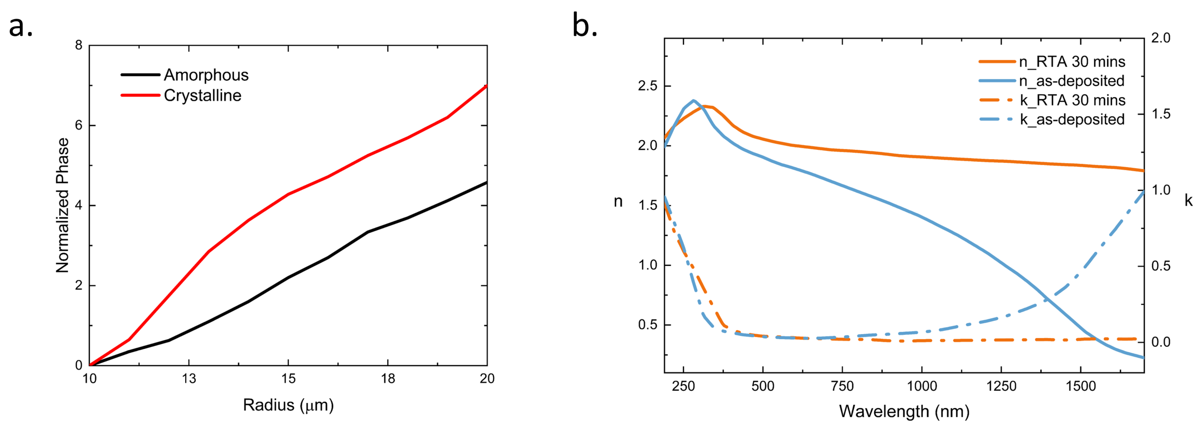
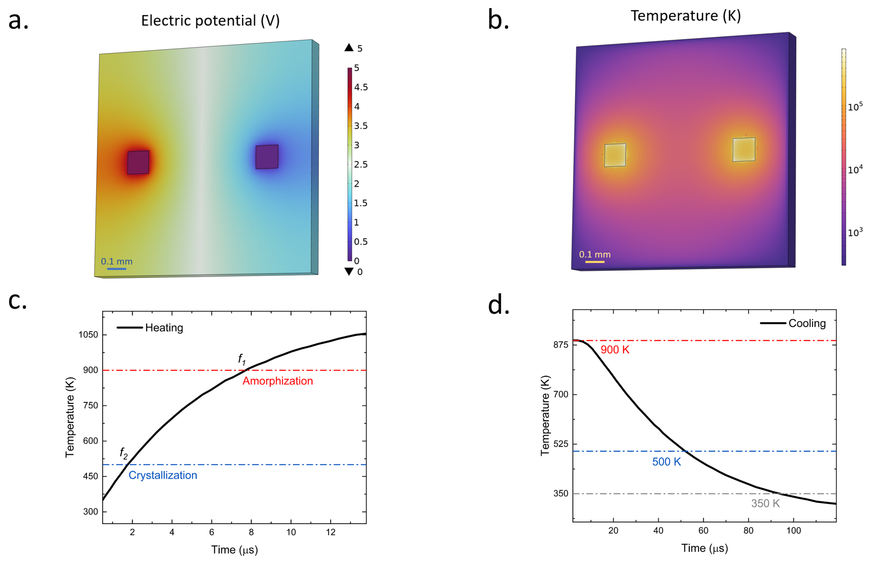
2.2. Simulation
2.3. Experiment
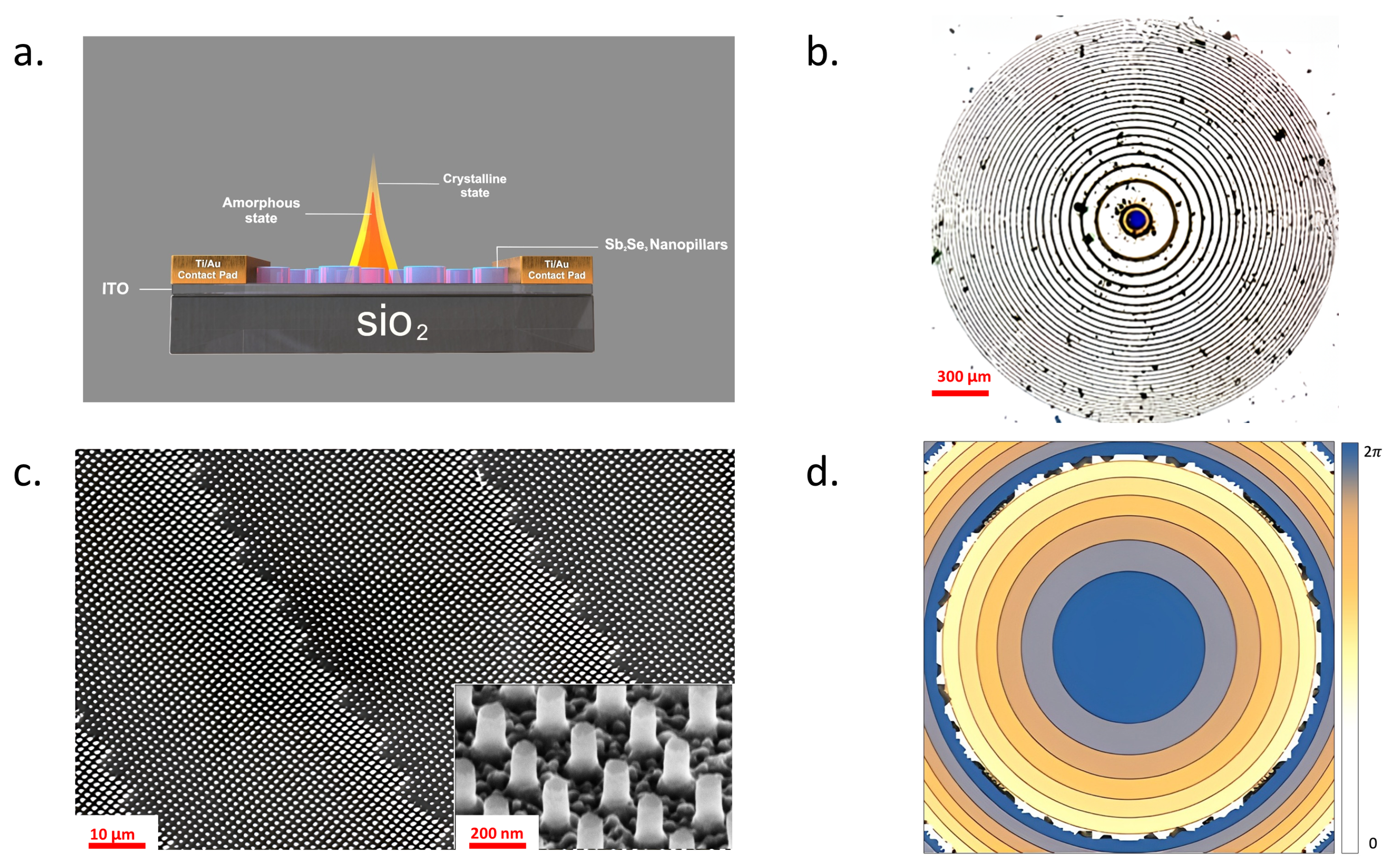
2.3.1. Device Fabrication
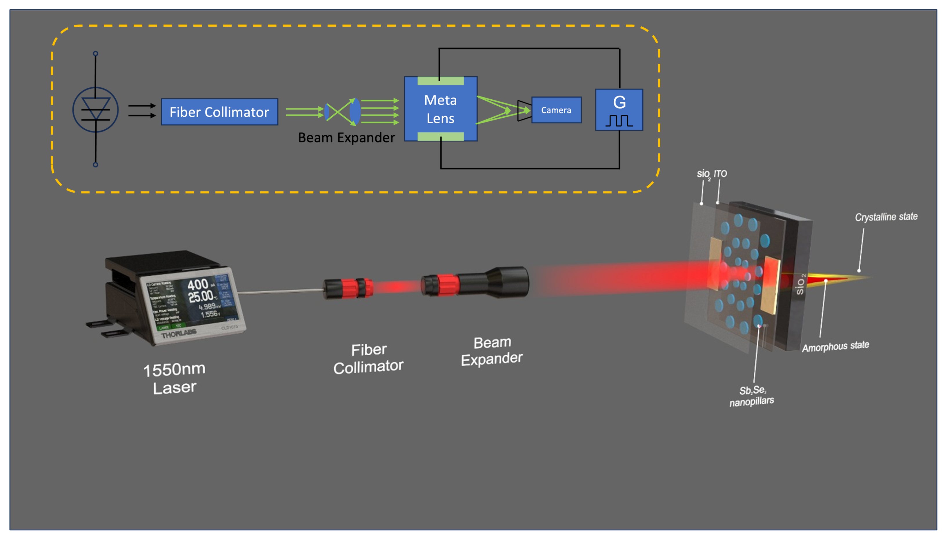
2.3.2. Experimental Setup
2.3.3. Focusing and Defocusing
2.3.4. Cyclability Test
3. Discussion
Author Contributions
Funding
Data Availability Statement
Acknowledgments
Conflicts of Interest
References
- Dana, D.; Duncan, W.M.; Slaughter, J. Emerging digital micromirror device (DMD) applications. In MOEMS Display and Imaging Systems; SPIE: Bellingham, DC, USA, 2003; Volume 4985. [Google Scholar]
- John, E.; Lee, B.L. Emerging Digital Micromirror Device Based Systems and Applications XII; SPIE: Bellingham, DC, USA, 2020; Volume 11294. [Google Scholar]
- Hornbeck, L.J. Current status of the digital micromirror device (DMD) for projection television applications. In Proceedings of the IEEE International Electron Devices Meeting, Washington, DC, USA, 5–8 December 1993; IEEE: Piscataway Township, NJ, USA, 1993. [Google Scholar]
- Sampsell, J.B. Digital micromirror device and its application to projection displays. J. Vac. Sci. Technol. Microelectron. Nanometer Struct. Process. Meas. Phenom. 1994, 12, 3242–3246. [Google Scholar] [CrossRef]
- Mario, M.; Sorger, V.J. Photonic tensor cores for machine learning. Appl. Phys. Rev. 2020, 7, 031404. [Google Scholar]
- Nicola, P.; Ma, X.; Shastri, B.J.; Sorger, V.J. Photonic tensor core for machine learning: A review. Emerg. Top. Artif. Intell. ETAI 2022, 12204, 53–60. [Google Scholar]
- Ye, J.; Solyanik, M.; Miscuglio, M.; Sorger, V. GHz-Fast Multiplexed OAM Generation and Detection. In Proceedings of the Frontiers in Optics 2020, Washington, DC, USA, 14–17 September; 2020. [Google Scholar] [CrossRef]
- Wang, H.; Dong, C.; Gui, Y.; Ye, J.; Altaleb, S.; Thomaschewski, M.; Movahhed Nouri, B.; Patil, C.; Dalir, H.; Sorger, V. Self-Powered Sb2Te3/MoS2 Heterojunction Broadband Photodetector on Flexible Substrate from Visible to Near Infrared. Nanomaterials 2023, 13, 1973. [Google Scholar] [CrossRef]
- Dalir, H.; Mokhtari-Koushyar, F.; Zand, I.; Heidari, E.; Xu, X.; Pan, Z.; Sun, S.; Amin, R.; Sorger, V.J.; Chen, R.T. Atto-Joule, high-speed, low-loss plasmonic modulator based on adiabatic coupled waveguides. Nanophotonics 2018, 7, 859–864. [Google Scholar] [CrossRef]
- Ye, J.; Solyanik, M.; Hu, Z.; Dalir, H.; Nouri, B.; Sorger, V. Free-space optical multiplexed orbital angular momentum beam identification system using Fourier optical convolutional layer based on 4f system. Complex Light Opt. Forces XVII 2023, 12436, 70–80. [Google Scholar]
- Mario, M.; Adam, G.C.; Kuzum, D.; Sorger, V.J. Roadmap on material-function mapping for photonic-electronic hybrid neural networks. APL Mater. 2019, 7, 100903. [Google Scholar]
- Andrea, F.; Dodson, C.M.; Rashid, Z.; Patrice, G.; Ewold, V.; Hatice, A. Nano-optics gets practical. Nat. Nanotechnol. 2015, 10, 11–15. [Google Scholar]
- Narayana, V.K.; Sun, S.; Badawy, A.A.; Sorger, V.J.; El-Ghazawi, T. MorphoNoC: Exploring the design space of a configurable hybrid NoC using nanophotonics. Microprocess. Microsystems 2017, 50, 113–126. [Google Scholar] [CrossRef] [Green Version]
- Amin, R.; George, J.H.; Wang, H.; Maiti, R.; Ma, Z.; Dalir, H.; Khurgin, J.B.; Sorger, V.J. An ITO–graphene heterojunction integrated absorption modulator on Si-photonics for neuromorphic nonlinear activation. APL Photonics 2021, 6, 120801. [Google Scholar] [CrossRef]
- Wang, H.; Gui, Y.; Heidari, E.; Kang, H.; Ye, J.; Dong, C.; Thomaschewski, M.; Nouri, B.M.; Dalir, H.; Sorger, V.J. Exploring the Potential of High-Speed 2D and 3D Materials in Silicon Photonics; SPIE: Philadelphia, PA, USA, 2023. [Google Scholar]
- Lin, R.J.; Su, V.; Wang, S.; Chen, M.K.; Chung, T.L.; Chen, Y.H.; Kuo, H.Y.; Chen, J.; Chen, J.; Huang, Y.; et al. Achromatic metalens array for full-colour light-field imaging. Nat. Nanotechnol. 2019, 14, 227–231. [Google Scholar] [CrossRef] [PubMed]
- Wang, S.; Wu, P.C.; Su, V.; Lai, Y.; Chen, M.; Kuo, H.Y.; Chen, B.H.; Chen, Y.H.; Huang, T.; Wang, J.; et al. A broadband achromatic metalens in the visible. Nat. Nanotechnol. 2018, 13, 227–232. [Google Scholar] [CrossRef] [PubMed]
- Chen, X.; Huang, L.; Mühlenbernd, H.; Li, G.; Bai, B.; Tan, Q.; Jin, G.; Qiu, C.; Zhang, S.; Zentgraf, T. Dual-polarity plasmonic metalens for visible light. Nat. Commun. 2012, 3, 1198. [Google Scholar] [CrossRef] [PubMed] [Green Version]
- Hsiao, H.; Chu, C.; Tsai, D. Fundamentals and applications of metasurfaces. Small Methods. 2017, 1, 1600064. [Google Scholar] [CrossRef] [Green Version]
- Engelberg, J.; Levy, U. The advantages of metalenses over diffractive lenses. Nat. Commun. 2020, 11, 1991. [Google Scholar] [CrossRef] [Green Version]
- Chen, W.T.; Zhu, A.Y.; Sanjeev, V.; Khorasaninejad, M.; Shi, Z.; Lee, E.; Capasso, F. A broadband achromatic metalens for focusing and imaging in the visible. Nat. Nanotechnol. 2018, 13, 220–226. [Google Scholar] [CrossRef] [Green Version]
- Khorasaninejad, M.; Chen, W.; Devlin, R.; Oh, J.; Zhu, A.; Capasso, F. Metalenses at visible wavelengths: Diffraction-limited focusing and subwavelength resolution imaging. Science 2016, 352, 1190–1194. [Google Scholar] [CrossRef] [Green Version]
- Moon, S.; Kim, Y.; Yoon, G.; Rho, J. Recent progress on ultrathin metalenses for flat optics. Iscience 2020, 23, 101877. [Google Scholar] [CrossRef]
- Afridi, A.; Canet-Ferrer, J.; Philippet, L.; Osmond, J.; Berto, P.; Quidant, R. Electrically driven varifocal silicon metalens. ACS Photonics 2018, 5, 4497–4503. [Google Scholar] [CrossRef] [Green Version]
- Pan, M.; Fu, Y.; Zheng, M.; Chen, H.; Zang, Y.; Duan, H.; Li, Q.; Qiu, M.; Hu, Y. Dielectric metalens for miniaturized imaging systems: Progress and challenges. Light. Sci. Appl. 2022, 11, 195. [Google Scholar] [CrossRef]
- Tseng, M.L.; Semmlinger, M.; Zhang, M.; Arndt, C.; Huang, T.T.; Yang, J.; Kuo, H.Y.; Su VY, F.; Chen, M.H.; Chu, C.H.; et al. Vacuum ultraviolet nonlinear metalens. Sci. Adv. 2022, 8, eabn5644. [Google Scholar] [CrossRef] [PubMed]
- Wang, Y.; Chen, Q.; Yang, W.; Ji, Z.; Jin, L.; Ma, X.; Song, Q.; Boltasseva, A.; Zhang, W.; Shalaev, V.M.; et al. High-efficiency broadband achromatic metalens for near-IR biological imaging window. Nat. Commun. 2021, 12, 5560. [Google Scholar] [CrossRef]
- Zhang, Y.; Chou, J.; Li, J.; Li, H.; Du, Q.; Yadav, A.; Zhou, S.; Shalaginov, M.; Fang, Z.; Zhong, H. Others Broadband transparent optical phase change materials for high-performance nonvolatile photonics. Nat. Commun. 2019, 10, 4279. [Google Scholar] [CrossRef] [PubMed] [Green Version]
- Shen, C.; Peserico, N.; Meng, J.; Ma, X.; Nouri, B.M.; Popescu, C.; Hu, J.; El-Ghazawi, T.; Dalir, H.; Sorger, V.J. Reconfigurable Application-Specific Photonic Integrated Circuit for solving Partial Differential Equations. arXiv 2022, arXiv:2208.03588. [Google Scholar]
- Shen, C.; Peserico, N.; Dalir, H.; Nouri, B.M.; Sorger, V.J. Power conservation version of application-specific photonic integrated circuit. In Smart Photonic and Optoelectronic Integrated Circuits; SPIE: Bellingham, DC, USA, 2023; Volume 12425. [Google Scholar]
- Wuttig, M.; Yamada, N. Phase-change materials for rewriteable data storage. Nat. Mater. 2007, 6, 824–832. [Google Scholar] [CrossRef] [PubMed]
- De Gracia, A.; Cabeza, L. Phase change materials and thermal energy storage for buildings. Energy Build. 2015, 103, 414–419. [Google Scholar] [CrossRef] [Green Version]
- Dutil, Y.; Rousse, D.; Salah, N.; Lassue, S.; Zalewski, L. A review on phase-change materials: Mathematical modeling and simulations. Renew. Sustain. Energy Rev. 2011, 15, 112–130. [Google Scholar] [CrossRef]
- Gu, T.; Kim, H.; Rivero-Baleine, C.; Hu, J. Reconfigurable metasurfaces towards commercial success. Nat. Photonics 2023, 17, 48–58. [Google Scholar] [CrossRef]
- Shalaginov, M.; An, S.; Zhang, Y.; Yang, F.; Su, P.; Liberman, V.; Chou, J.; Roberts, C.; Kang, M.; Rios, C.; et al. Reconfigurable all-dielectric metalens with diffraction-limited performance. Nat. Commun. 2021, 12, 1225. [Google Scholar] [CrossRef]
- Wang, M.; Lee, J.S.; Aggarwal, S.; Farmakidis, N.; He, Y.; Cheng, T.; Bhaskaran, H. Varifocal Metalens Using Tunable and Ultralow-loss Dielectrics. Adv. Sci. 2023, 10, 2204899. [Google Scholar] [CrossRef]
- Kamali, S.; Arbabi, E.; Arbabi, A.; Faraon, A. A review of dielectric optical metasurfaces for wavefront control. Nanophotonics 2018, 7, 1041–1068. [Google Scholar] [CrossRef]
- Raoux, S. Phase change materials. Annu. Rev. Mater. Res. 2009, 39, 25–48. [Google Scholar] [CrossRef]
- Mavlonov, A.; Razykov, T.; Raziq, F.; Gan, J.; Chantana, J.; Kawano, Y.; Nishimura, T.; Wei, H.; Zakutayev, A.; Minemoto, T. A review of Sb2Se3 photovoltaic absorber materials and thin-film solar cells. Sol. Energy 2020, 201, 227–246. [Google Scholar] [CrossRef]
- Tahersima, M.H.; Sorger, V.J. Enhanced photon absorption in spiral nanostructured solar cells using layered 2D materials. Nanotechnology 2015, 26, 344005. [Google Scholar] [CrossRef] [PubMed] [Green Version]
- Tahersima, M.H.; Ma, Z.; Gui, Y.; Sun, S.; Wang, H.; Amin, R.; Dalir, H.; Chen, R.; Miscuglio, M.; Sorger, V.J. Coupling-enhanced dual ITO layer electro-absorption modulator in silicon photonics. Nanophotonics 2019, 8, 1559–1566. [Google Scholar] [CrossRef]
- Amin, R.; Maiti, R.; Gui, Y.; Suer, C.; Miscuglio, M.; Heidari, E.; Khurgin, J.B.; Chen, R.T.; Sorger, H.D.V.J. Heterogeneously integrated ITO plasmonic Mach–Zehnder interferometric modulator on SOI. Sci. Rep. 2021, 11, 1287. [Google Scholar] [CrossRef]
- Kato, K.; Kuwahara, M.; Kawashima, H.; Tsuruoka, T.; Tsuda, H. Current-driven phase-change optical gate switch using indium–tin-oxide heater. Appl. Phys. Express 2017, 10, 072201. [Google Scholar] [CrossRef]
- Ahmed, M.; Bakry, A.; Qasem, A.; Dalir, H. The main role of thermal annealing in controlling the structural and optical properties of ITO thin film layer. Opt. Mater. 2021, 113, 110866. [Google Scholar] [CrossRef]
- Ahmed, M.; Bakry, A.; Shaaban, E.R.; Dalir, H. Structural, electrical, and optical properties of ITO thin films and their influence on performance of CdS/CdTe thin-film solar cells. J. Mater. Sci. Mater. Electron. 2021, 32, 11107–11118. [Google Scholar] [CrossRef]
- Zanotto, S.; Blancato, A.; Buchheit, A.; Muñoz-Castro, M.; Wiemhöfer, H.; Morichetti, F.; Melloni, A. Metasurface Reconfiguration through Lithium-Ion Intercalation in a Transition Metal Oxide. Adv. Opt. Mater. 2017, 5, 1600732. [Google Scholar] [CrossRef] [Green Version]
- COMSOL Multiphysics. Introduction to COMSOL Multiphysics®; COMSOL Multiphysics: Burlington, MA, USA, 1998. [Google Scholar]
- Gui, Y.; Miscuglio, M.; Ma, Z.; Tahersima, M.H.; Sun, S.; Amin, R.; Sorger, H.D.V.J. Towards integrated metatronics: A holistic approach on precise optical and electrical properties of indium tin oxide. Sci. Rep. 2019, 9, 11279. [Google Scholar] [CrossRef] [PubMed] [Green Version]
- Safi, I. Recent aspects concerning DC reactive magnetron sputtering of thin films: A review. Surf. Coat. Technol. 2000, 127, 203–218. [Google Scholar] [CrossRef]
- Laermer, F.; Andrea, U. Challenges, developments and applications of silicon deep reactive ion etching. Microelectron. Eng. 2003, 67, 349–355. [Google Scholar] [CrossRef]
Disclaimer/Publisher’s Note: The statements, opinions and data contained in all publications are solely those of the individual author(s) and contributor(s) and not of MDPI and/or the editor(s). MDPI and/or the editor(s) disclaim responsibility for any injury to people or property resulting from any ideas, methods, instructions or products referred to in the content. |
© 2023 by the authors. Licensee MDPI, Basel, Switzerland. This article is an open access article distributed under the terms and conditions of the Creative Commons Attribution (CC BY) license (https://creativecommons.org/licenses/by/4.0/).
Share and Cite
Shen, C.; Ye, J.; Peserico, N.; Gui, Y.; Dong, C.; Kang, H.; Movahhed Nouri, B.; Wang, H.; Heidari, E.; Sorger, V.J.; et al. Enhancing Focusing and Defocusing Capabilities with a Dynamically Reconfigurable Metalens Utilizing Sb2Se3 Phase-Change Material. Nanomaterials 2023, 13, 2106. https://doi.org/10.3390/nano13142106
Shen C, Ye J, Peserico N, Gui Y, Dong C, Kang H, Movahhed Nouri B, Wang H, Heidari E, Sorger VJ, et al. Enhancing Focusing and Defocusing Capabilities with a Dynamically Reconfigurable Metalens Utilizing Sb2Se3 Phase-Change Material. Nanomaterials. 2023; 13(14):2106. https://doi.org/10.3390/nano13142106
Chicago/Turabian StyleShen, Chen, Jiachi Ye, Nicola Peserico, Yaliang Gui, Chaobo Dong, Haoyan Kang, Behrouz Movahhed Nouri, Hao Wang, Elham Heidari, Volker J. Sorger, and et al. 2023. "Enhancing Focusing and Defocusing Capabilities with a Dynamically Reconfigurable Metalens Utilizing Sb2Se3 Phase-Change Material" Nanomaterials 13, no. 14: 2106. https://doi.org/10.3390/nano13142106