
Spatiotemporal Visualization of Photogenerated Carriers on an Avalanche Photodiode Surface Using Ultrafast Scanning Electron Microscopy
 , and
, and 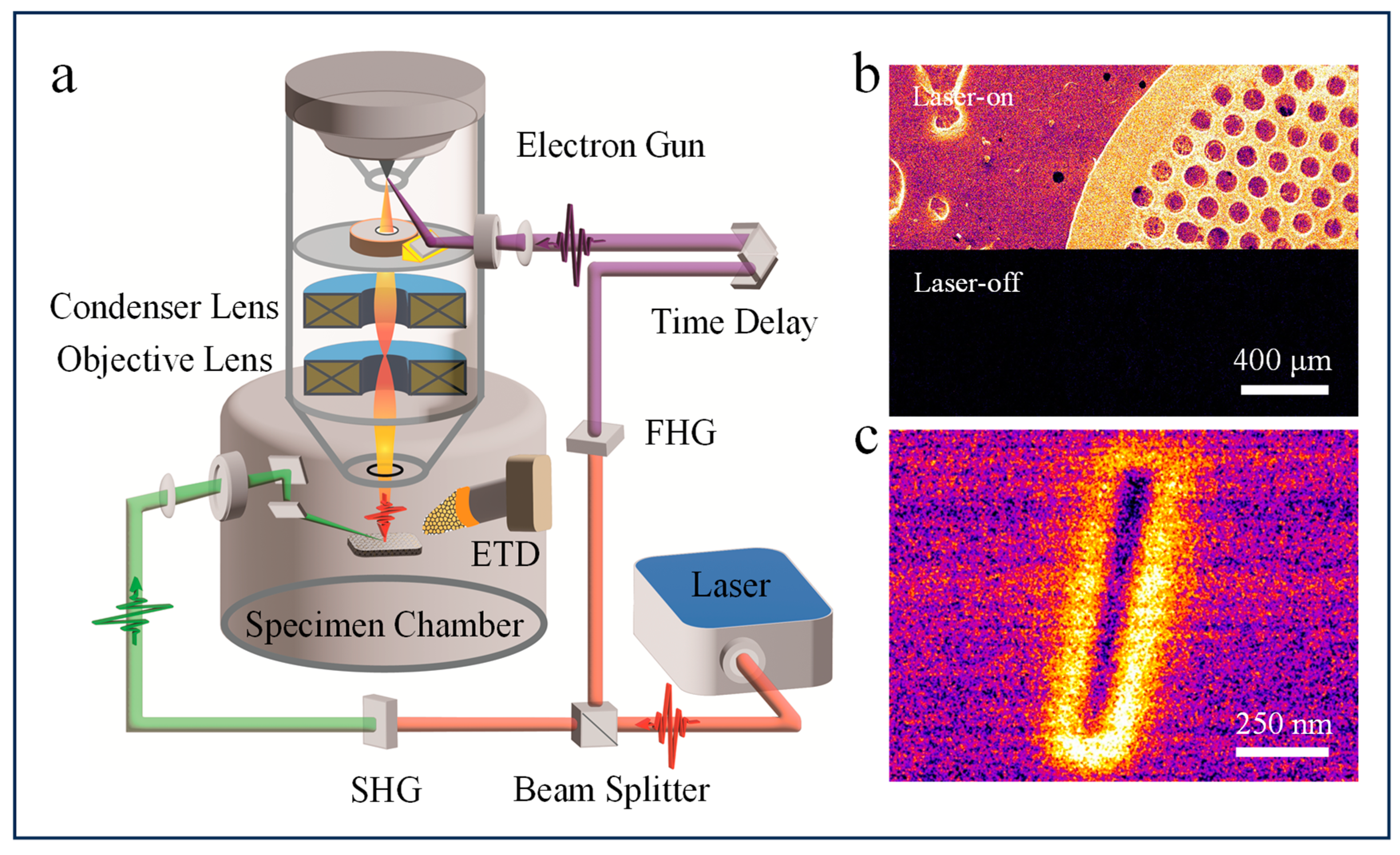
Abstract
:1. Introduction
2. Materials and Methods
2.1. Instruments
2.2. Materials and Methods
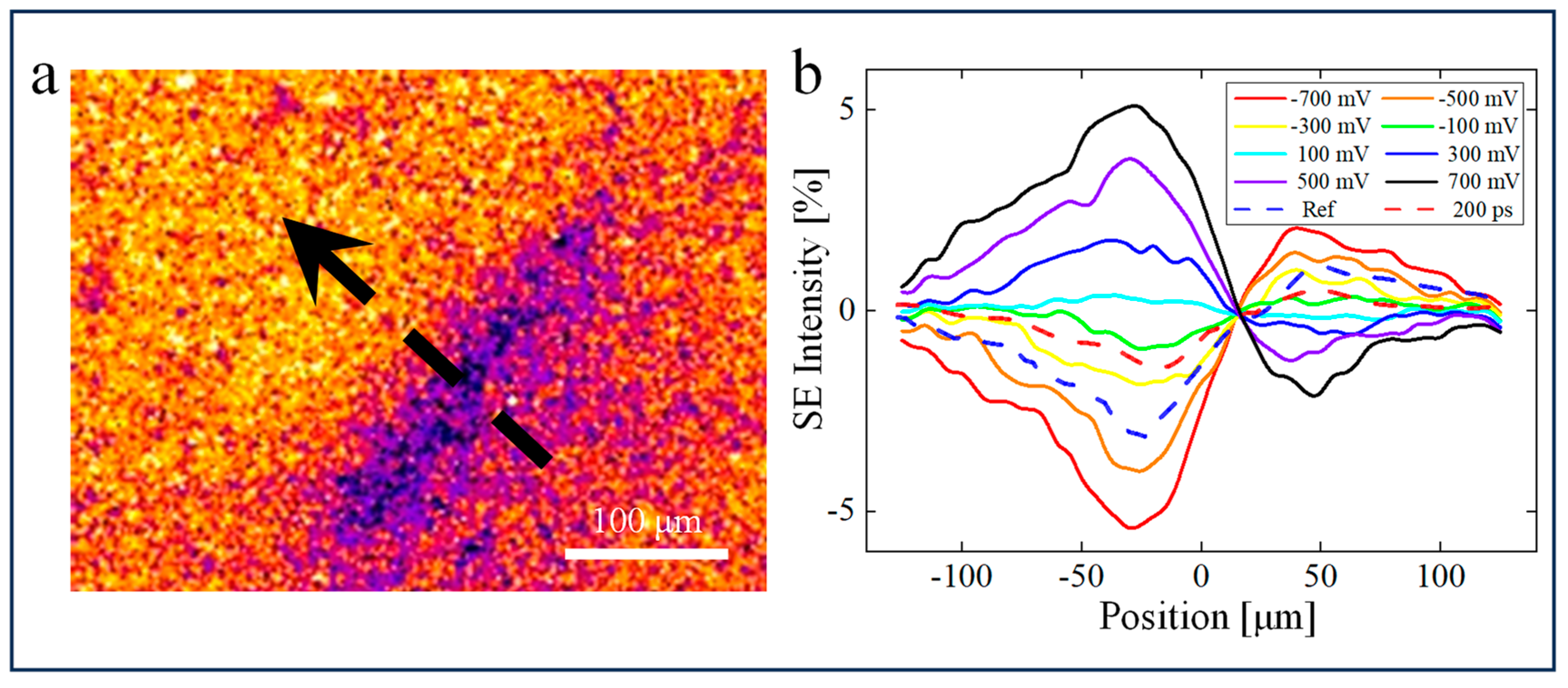
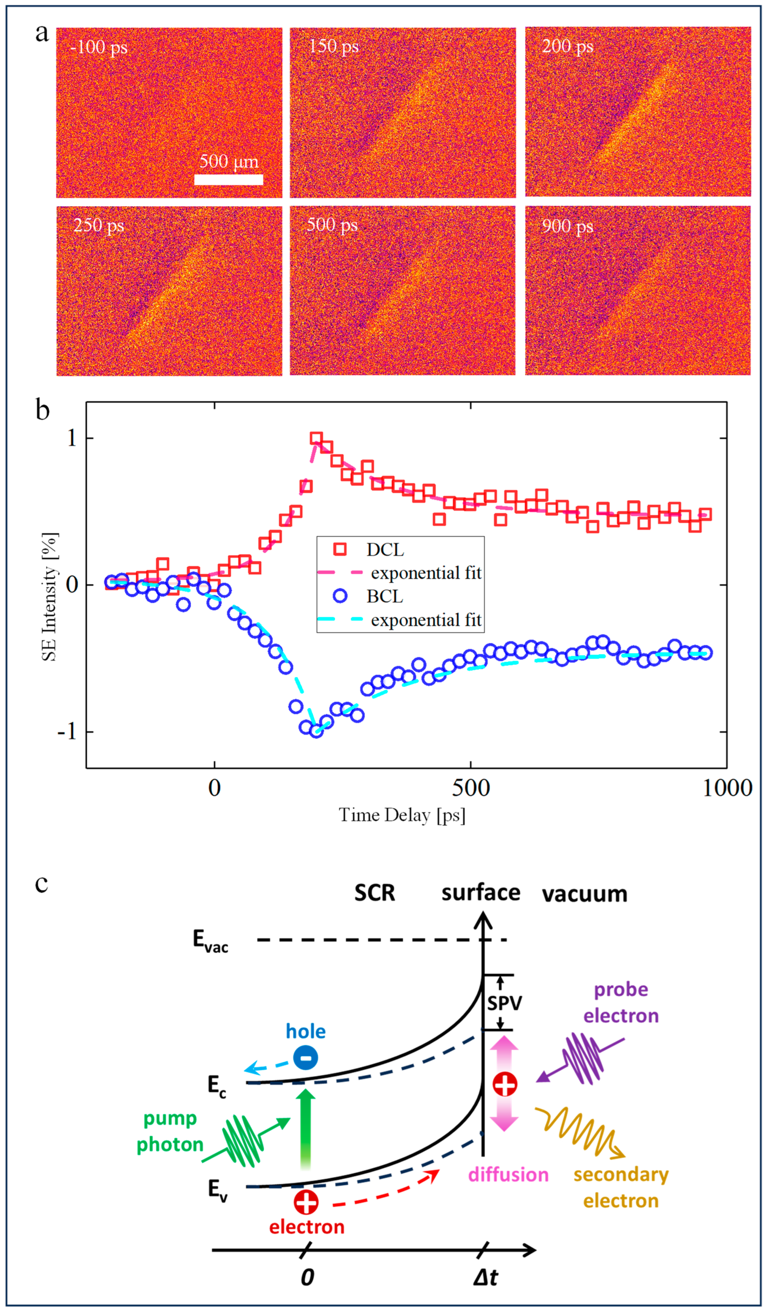
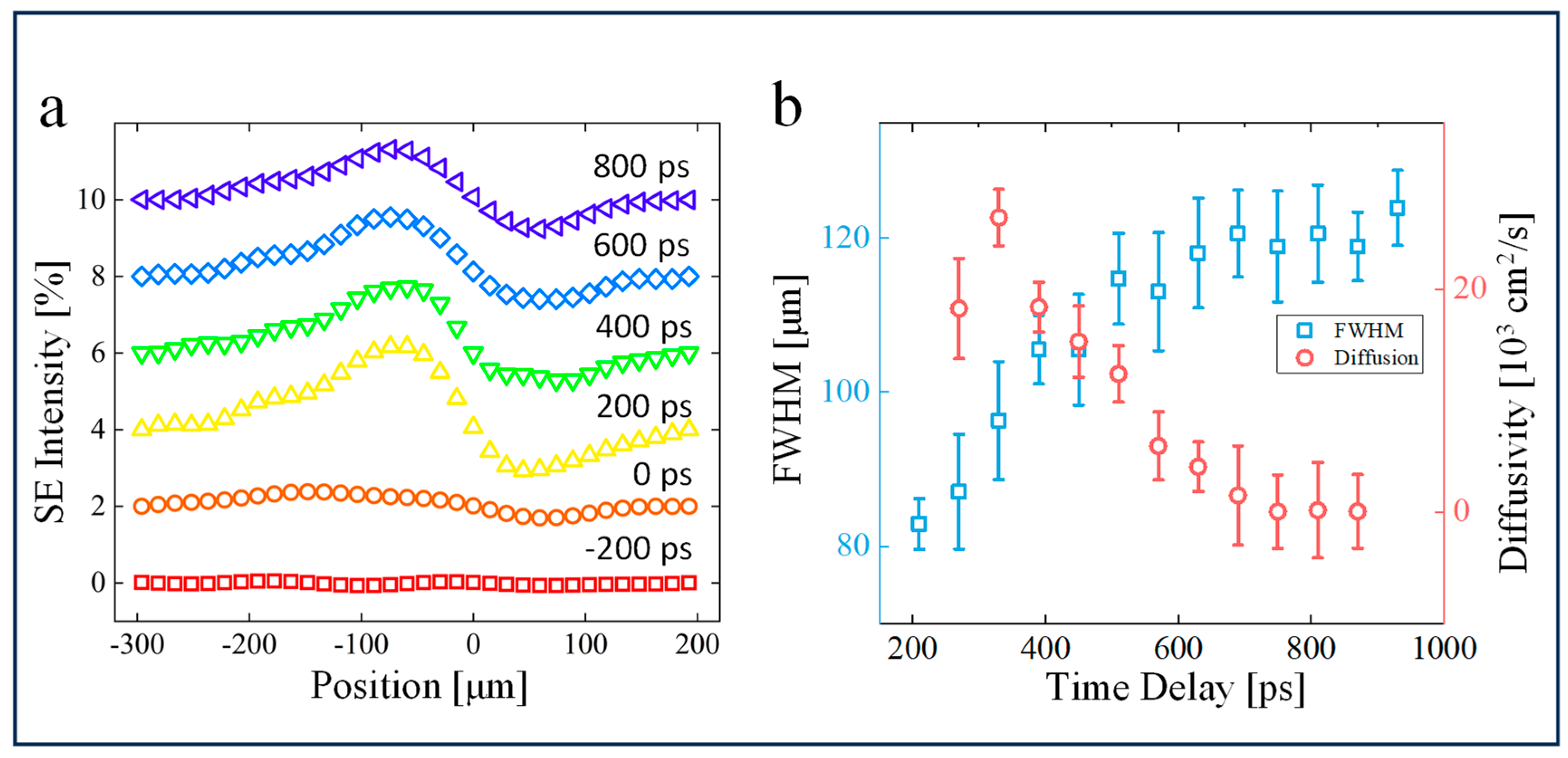
3. Results and Discussion
4. Conclusions
Supplementary Materials
Author Contributions
Funding
Data Availability Statement
Acknowledgments
Conflicts of Interest
References
- Qian, R.; Zong, H.; Schneider, J.; Zhou, G.; Zhao, T.; Li, Y.; Yang, J.; Bahnemann, D.W.; Pan, J.H. Charge carrier trapping, recombination and transfer during TiO2 photocatalysis: An overview. Catal. Today 2019, 335, 78–90. [Google Scholar] [CrossRef]
- Li, S.; Xu, W.; Meng, L.; Tian, W.; Li, L. Recent Progress on Semiconductor Heterojunction-Based Photoanodes for Photoelectrochemical Water Splitting. Small Sci. 2022, 2, 2100112. [Google Scholar] [CrossRef]
- Fratini, S.; Nikolka, M.; Salleo, A.; Schweicher, G.; Sirringhaus, H. Charge transport in high-mobility conjugated polymers and molecular semiconductors. Nat. Mater. 2020, 19, 491–502. [Google Scholar] [CrossRef]
- Zhao, J.; Nughays, R.; Bakr, O.M.; Mohammed, O.F. Access to Ultrafast Surface and Interface Carrier Dynamics Simultaneously in Space and Time. J. Phys. Chem. C 2021, 125, 14495–14516. [Google Scholar] [CrossRef]
- Yang, Y.; Gu, J.; Young, J.L.; Miller, E.M.; Turner, J.A.; Neale, N.R.; Beard, M.C. Semiconductor interfacial carrier dynamics via photoinduced electric fields. Science 2015, 350, 1061–1065. [Google Scholar] [CrossRef]
- Samanta, C.; Ghatak, A.; Raychaudhuri, A.K.; Ghosh, B. Surface/Interface Defect Engineering on Charge Carrier Transport toward Broadband (UV-NIR) Photoresponse in the Heterostructure Array of p-Si NWs/ZnO Photodetector. ACS Appl. Electron. Mater. 2023, 5, 865–876. [Google Scholar] [CrossRef]
- Campbell, J.C. Recent Advances in Avalanche Photodiodes. J. Light. Technol. 2016, 34, 278–285. [Google Scholar] [CrossRef]
- Martyniuk, P.; Wang, P.; Rogalski, A.; Gu, Y.; Jiang, R.; Wang, F.; Hu, W. Infrared avalanche photodiodes from bulk to 2D materials. Light Sci. Appl. 2023, 12, 212. [Google Scholar] [CrossRef]
- Yu, Y.; Liu, B.; Chen, Z. Analyzing the performance of pseudo-random single photon counting ranging Lidar. Appl. Opt. 2018, 57, 7733–7739. [Google Scholar] [CrossRef]
- Zhao, B.; Wang, F.; Chen, H.; Wang, Y.; Jiang, M.; Fang, X.; Zhao, D. Solar-Blind Avalanche Photodetector Based on Single ZnO–Ga2O3 Core–Shell Microwire. Nano Lett. 2015, 15, 3988–3993. [Google Scholar] [CrossRef]
- Zhou, M.; Wang, W.; Qu, H.; Han, H.; Zhu, Y.; Guo, Z.; Gui, L.; Wang, X.; Lu, W. InGaAsP/InP single photon avalanche diodes with ultra-high photon detection efficiency. Opt. Quantum Electron. 2020, 52, 299. [Google Scholar] [CrossRef]
- Chen, Y.; Zhang, Z.; Miao, G.; Jiang, H.; Song, H. A comparative study of front- and back-illuminated planar InGaAs/InP avalanche photodiodes. Mater. Lett. 2022, 308, 131144. [Google Scholar] [CrossRef]
- Zhang, J.; Li, X.; Du, C.; Jiang, Y.; Ma, Z.; Chen, H.; Jia, H.; Wang, W.; Deng, Z. Experimental Demonstration of the Impact of the Parameters of Floating Guard Ring on Planar InP/InGaAs-Based Avalanche Photodiodes’ Performance and Its Optimization. IEEE Photonics J. 2022, 14, 2218406. [Google Scholar] [CrossRef]
- Zhao, Y.; Chen, J. InGaAs/InP SAGCM avalanche photodiode with a heterojunction multiplication layer. Phys. B Condens. Matter 2022, 629, 413637. [Google Scholar] [CrossRef]
- Grumstrup, E.M.; Gabriel, M.M.; Cating, E.E.M.; Van Goethem, E.M.; Papanikolas, J.M. Pump–probe microscopy: Visualization and spectroscopy of ultrafast dynamics at the nanoscale. Chem. Phys. 2015, 458, 30–40. [Google Scholar] [CrossRef]
- Vazquez, G.D.B.; Morganti, G.L.G.; Block, A.; van Hulst, N.F.; Liebel, M.; Tielrooij, K.-J. Spatiotemporal Microscopy: Shining Light on Transport Phenomena. Adv. Electron. Mater. 2023, 2300584. [Google Scholar] [CrossRef]
- Cabanillas-Gonzalez, J.; Grancini, G.; Lanzani, G. Pump-probe spectroscopy in organic semiconductors: Monitoring fundamental processes of relevance in optoelectronics. Adv. Mater. 2011, 23, 5468–5485. [Google Scholar] [CrossRef]
- Tagliabue, G.; DuChene, J.S.; Abdellah, M.; Habib, A.; Gosztola, D.J.; Hattori, Y.; Cheng, W.-H.; Zheng, K.; Canton, S.E.; Sundararaman, R.; et al. Ultrafast hot-hole injection modifies hot-electron dynamics in Au/p-GaN heterostructures. Nat. Mater. 2020, 19, 1312–1318. [Google Scholar] [CrossRef]
- Gross, N.; Kuhs, C.T.; Ostovar, B.; Chiang, W.-Y.; Wilson, K.S.; Volek, T.S.; Faitz, Z.M.; Carlin, C.C.; Dionne, J.A.; Zanni, M.T.; et al. Progress and Prospects in Optical Ultrafast Microscopy in the Visible Spectral Region: Transient Absorption and Two-Dimensional Microscopy. J. Phys. Chem. C 2023, 127, 14557–14586. [Google Scholar] [CrossRef]
- Reimer, L. Scanning Electron Microscopy: Physics of Image Formation and Microanalysis, Second Edition. Meas. Sci. Technol. 2000, 11, 1826. [Google Scholar] [CrossRef]
- May, P.; Halbout, J.M.; Chiu, G. Picosecond photoelectron scanning electron microscope for noncontact testing of integrated circuits. Appl. Phys. Lett. 1987, 51, 145–147. [Google Scholar] [CrossRef]
- Yang, D.-S.; Mohammed, O.F.; Zewail, A.H. Scanning ultrafast electron microscopy. Proc. Natl. Acad. Sci. USA 2010, 107, 14993–14998. [Google Scholar] [CrossRef]
- Sun, J.; Adhikari, A.; Shaheen, B.S.; Yang, H.; Mohammed, O.F. Mapping Carrier Dynamics on Material Surfaces in Space and Time using Scanning Ultrafast Electron Microscopy. J. Phys. Chem. Lett. 2016, 7, 985–994. [Google Scholar] [CrossRef]
- Garming, M.W.H.; Weppelman, I.G.C.; Lee, M.; Stavenga, T.; Hoogenboom, J.P. Ultrafast scanning electron microscopy with sub-micrometer optical pump resolution. Appl. Phys. Rev. 2022, 9, 021418. [Google Scholar] [CrossRef]
- Zewail, A.H. Four-Dimensional Electron Microscopy. Science 2010, 328, 187–193. [Google Scholar] [CrossRef]
- Zhu, C.; Zheng, D.; Wang, H.; Zhang, M.; Li, Z.; Sun, S.; Xu, P.; Tian, H.; Li, Z.; Yang, H.; et al. Development of analytical ultrafast transmission electron microscopy based on laser-driven Schottky field emission. Ultramicroscopy 2020, 209, 112887. [Google Scholar] [CrossRef]
- Sundaram, S.K.; Mazur, E. Inducing and probing non-thermal transitions in semiconductors using femtosecond laser pulses. Nat. Mater. 2002, 1, 217–224. [Google Scholar] [CrossRef]
- Kronik, L.; Shapira, Y. Surface photovoltage spectroscopy of semiconductor structures: At the crossroads of physics, chemistry and electrical engineering. Surf. Interface Anal. 2001, 31, 954–965. [Google Scholar] [CrossRef]
- Sun, J.; Melnikov, V.A.; Khan, J.I.; Mohammed, O.F. Real-Space Imaging of Carrier Dynamics of Materials Surfaces by Second-Generation Four-Dimensional Scanning Ultrafast Electron Microscopy. J. Phys. Chem. Lett. 2015, 6, 3884–3890. [Google Scholar] [CrossRef] [PubMed]
- Zani, M.; Sala, V.; Irde, G.; Pietralunga, S.M.; Manzoni, C.; Cerullo, G.; Lanzani, G.; Tagliaferri, A. Charge dynamics in aluminum oxide thin film studied by ultrafast scanning electron microscopy. Ultramicroscopy 2018, 187, 93–97. [Google Scholar] [CrossRef] [PubMed]
- Zhang, L.; Hoogenboom, J.P.; Cook, B.; Kruit, P. Photoemission sources and beam blankers for ultrafast electron microscopy. Struct. Dyn. 2019, 6, 051501. [Google Scholar] [CrossRef] [PubMed]
- Merano, M.; Sonderegger, S.; Crottini, A.; Collin, S.; Renucci, P.; Pelucchi, E.; Malko, A.; Baier, M.H.; Kapon, E.; Deveaud, B.; et al. Probing carrier dynamics in nanostructures by picosecond cathodoluminescence. Nature 2005, 438, 479–482. [Google Scholar] [CrossRef] [PubMed]
- Morishita, H.; Ohshima, T.; Otsuga, K.; Kuwahara, M.; Agemura, T.; Ose, Y. Brightness evaluation of pulsed electron gun using negative electron affinity photocathode developed for time-resolved measurement using scanning electron microscope. Ultramicroscopy 2021, 230, 113386. [Google Scholar] [CrossRef] [PubMed]
- Gerbig, C.; Senftleben, A.; Morgenstern, S.; Sarpe, C.; Baumert, T. Spatio-temporal resolution studies on a highly compact ultrafast electron diffractometer. New J. Phys. 2015, 17, 043050. [Google Scholar] [CrossRef]
- Cho, J.; Hwang, T.Y.; Zewail, A.H. Visualization of carrier dynamics in p(n)-type GaAs by scanning ultrafast electron microscopy. Proc. Natl. Acad. Sci. USA 2014, 111, 2094–2099. [Google Scholar] [CrossRef] [PubMed]
- Bose, R.; Sun, J.; Khan, J.I.; Shaheen, B.S.; Adhikari, A.; Ng, T.K.; Burlakov, V.M.; Parida, M.R.; Priante, D.; Goriely, A.; et al. Real-Space Visualization of Energy Loss and Carrier Diffusion in a Semiconductor Nanowire Array Using 4D Electron Microscopy. Adv. Mater. 2016, 28, 5106–5111. [Google Scholar] [CrossRef] [PubMed]
- Bose, R.; Bera, A.; Parida, M.R.; Adhikari, A.; Shaheen, B.S.; Alarousu, E.; Sun, J.; Wu, T.; Bakr, O.M.; Mohammed, O.F. Real-Space Mapping of Surface Trap States in CIGSe Nanocrystals Using 4D Electron Microscopy. Nano Lett. 2016, 16, 4417–4423. [Google Scholar] [CrossRef]
- Najafi, E.; Ivanov, V.; Zewail, A.; Bernardi, M. Super-diffusion of excited carriers in semiconductors. Nat. Commun. 2017, 8, 15177. [Google Scholar] [CrossRef]
- Liao, B.; Zhao, H.; Najafi, E.; Yan, X.; Tian, H.; Tice, J.; Minnich, A.J.; Wang, H.; Zewail, A.H. Spatial-Temporal Imaging of Anisotropic Photocarrier Dynamics in Black Phosphorus. Nano Lett. 2017, 17, 3675–3680. [Google Scholar] [CrossRef]
- Shaheen, B.S.; El-Zohry, A.M.; Yin, J.; De Bastiani, M.; De Wolf, S.; Bakr, O.M.; Mohammed, O.F. Visualization of Charge Carrier Trapping in Silicon at the Atomic Surface Level Using Four-Dimensional Electron Imaging. J. Phys. Chem. Lett. 2019, 10, 1960–1966. [Google Scholar] [CrossRef]
- Ellis, S.R.; Bartelt, N.C.; Léonard, F.; Celio, K.C.; Fuller, E.J.; Hughart, D.R.; Garland, D.; Marinella, M.J.; Michael, J.R.; Chandler, D.W.; et al. Scanning ultrafast electron microscopy reveals photovoltage dynamics at a deeply buried p-Si/SiO2 interface. Phys. Rev. B 2021, 104, L161303. [Google Scholar] [CrossRef]
- Najafi, E.; Jafari, A. Ultrafast imaging of surface-exclusive carrier dynamics in silicon. J. Appl. Phys. 2019, 125, 185303. [Google Scholar] [CrossRef]
- Li, Y.; Choudhry, U.; Ranasinghe, J.; Ackerman, A.; Liao, B. Probing Surface Photovoltage Effect Using Photoassisted Secondary Electron Emission. J. Phys. Chem. A 2020, 124, 5246–5252. [Google Scholar] [CrossRef] [PubMed]
- Ouyang, W.; Zuo, X.; Liao, B. Impact of photoexcitation on secondary electron emission: A Monte Carlo study. J. Appl. Phys. 2023, 133, 064301. [Google Scholar] [CrossRef]
- Irde, G.; Pietralunga, S.M.; Sala, V.; Zani, M.; Ball, J.M.; Barker, A.J.; Petrozza, A.; Lanzani, G.; Tagliaferri, A. Imaging photoinduced surface potentials on hybrid perovskites by real-time Scanning Electron Microscopy. Micron 2019, 121, 53–65. [Google Scholar] [CrossRef] [PubMed]
- Zaghloul, M.; Pietralunga, S.M.; Irde, G.; Sala, V.; Cerullo, G.; Chen, H.; Isella, G.; Lanzani, G.; Zani, M.; Tagliaferri, A. Dynamical imaging of local photovoltage at semiconductor surface by photo-assisted ultrafast scanning electron microscopy. EPJ Web Conf. 2021, 255, 11001. [Google Scholar] [CrossRef]
- Garming, M.W.H.; Bolhuis, M.; Conesa-Boj, S.; Kruit, P.; Hoogenboom, J.P. Lock-in Ultrafast Electron Microscopy Simultaneously Visualizes Carrier Recombination and Interface-Mediated Trapping. J. Phys. Chem. Lett. 2020, 11, 8880–8886. [Google Scholar] [CrossRef]
- Leibovitch, M.; Kronik, L.; Mishori, B.; Shapira, Y.; Hanson, C.M.; Clawson, A.R.; Ram, P. Determining band offsets using surface photovoltage spectroscopy: The InP/In0.53Ga0.47As heterojunction. Appl. Phys. Lett. 1996, 69, 2587–2589. [Google Scholar] [CrossRef]
- Lee, H.J.; Gamel, M.M.A.; Ker, P.J.; Jamaludin, M.Z.; Wong, Y.H.; David, J.P.R. Absorption Coefficient of Bulk III-V Semiconductor Materials: A Review on Methods, Properties and Future Prospects. J. Electron. Mater. 2022, 51, 6082–6107. [Google Scholar] [CrossRef]
- Tarbi, A.; Chtouki, T.; Bouich, A.; Elkouari, Y.; Erguig, H.; Migalska-Zalas, A.; Aissat, A. InP/InGaAsP thin films based solar cells: Lattice mismatch impact on efficiency. Opt. Mater. 2022, 131, 112704. [Google Scholar] [CrossRef]
- Block, A.; Liebel, M.; Yu, R.; Spector, M.; Sivan, Y.; García de Abajo, F.J.; van Hulst, N.F. Tracking ultrafast hot-electron diffusion in space and time by ultrafast thermomodulation microscopy. Sci. Adv. 2019, 5, eaav8965. [Google Scholar] [CrossRef] [PubMed]
- Sotoodeh, M.; Khalid, A.H.; Rezazadeh, A.A. Empirical low-field mobility model for III–V compounds applicable in device simulation codes. J. Appl. Phys. 2000, 87, 2890–2900. [Google Scholar] [CrossRef]
- Najafi, E.; Scarborough, T.D.; Tang, J.; Zewail, A. Four-dimensional imaging of carrier interface dynamics in p-n junctions. Science 2015, 347, 164–167. [Google Scholar] [CrossRef] [PubMed]
- Nughays, R.O.; Yang, C.; Nematulloev, S.; Yin, J.; Harrison, G.T.; Zhao, J.; Fatayer, S.; Bakr, O.M.; Mohammed, O.F. Visualization of Surface Charge Carrier Diffusion Lengths in Different Perovskite Crystal Orientations Using 4D Electron Imaging. Adv. Opt. Mater. 2023, 11, 2300190. [Google Scholar] [CrossRef]

Disclaimer/Publisher’s Note: The statements, opinions and data contained in all publications are solely those of the individual author(s) and contributor(s) and not of MDPI and/or the editor(s). MDPI and/or the editor(s) disclaim responsibility for any injury to people or property resulting from any ideas, methods, instructions or products referred to in the content. |
© 2024 by the authors. Licensee MDPI, Basel, Switzerland. This article is an open access article distributed under the terms and conditions of the Creative Commons Attribution (CC BY) license (https://creativecommons.org/licenses/by/4.0/).
Share and Cite
Tian, Y.; Yang, D.; Ma, Y.; Li, Z.; Li, J.; Deng, Z.; Tian, H.; Yang, H.; Sun, S.; Li, J. Spatiotemporal Visualization of Photogenerated Carriers on an Avalanche Photodiode Surface Using Ultrafast Scanning Electron Microscopy. Nanomaterials 2024, 14, 310. https://doi.org/10.3390/nano14030310
Tian Y, Yang D, Ma Y, Li Z, Li J, Deng Z, Tian H, Yang H, Sun S, Li J. Spatiotemporal Visualization of Photogenerated Carriers on an Avalanche Photodiode Surface Using Ultrafast Scanning Electron Microscopy. Nanomaterials. 2024; 14(3):310. https://doi.org/10.3390/nano14030310
Chicago/Turabian StyleTian, Yuan, Dong Yang, Yu Ma, Zhongwen Li, Jun Li, Zhen Deng, Huanfang Tian, Huaixin Yang, Shuaishuai Sun, and Jianqi Li. 2024. "Spatiotemporal Visualization of Photogenerated Carriers on an Avalanche Photodiode Surface Using Ultrafast Scanning Electron Microscopy" Nanomaterials 14, no. 3: 310. https://doi.org/10.3390/nano14030310