
Characterization of Mn5Ge3 Contacts on a Shallow Ge/SiGe Heterostructure


1
Sandia National Laboratories, Albuquerque, NM 87185, USA
2
Center for Integrated Nanotechnologies, Albuquerque, NM 87185, USA
3
Center for High Technology Materials, University of New Mexico, Albuquerque, NM 87106, USA
*
Author to whom correspondence should be addressed.
Nanomaterials 2024, 14(6), 539; https://doi.org/10.3390/nano14060539
Submission received: 26 January 2024
/
Revised: 14 March 2024
/
Accepted: 15 March 2024
/
Published: 19 March 2024
(This article belongs to the Special Issue Advanced Spintronic and Electronic Nanomaterials)
Abstract
: is a ferromagnetic phase of the Mn-Ge system that is a potential contact material for efficient spin injection and detection. Here, we investigate the creation of -based contacts on a Ge/SiGe quantum well heterostructure via solid-state synthesis. X-ray diffraction spectra fitting indicates the formation of -based contacts on bulk Ge and Ge/SiGe. High-resolution scanning transmission electron microscopy imaging and energy dispersive X-ray spectroscopy verify the correct -based phase formation. Schottky diode measurements, transmission line measurements, and Hall measurements reveal that -based contacts serve as good p-type contacts for Ge/SiGe quantum well heterostructures due to having a low Schottky barrier height of (extracted from a /n-Ge analogue) and a contact resistance in the order of 1 . Furthermore, we show that these electrical characteristics have a gate-voltage dependence, thereby providing tunability.
1. Introduction
Holes in germanium (Ge) have been shown to be an excellent candidate for spin-based alternative computing technologies, such as spin field-effect transistors (SpinFETs) for classical computing [1,2,3] and hole spin qubits for quantum computing [4,5,6,7,8,9,10]. In either technology, it is paramount to start with the best possible material. Recently, there have been demonstrations of Ge/SiGe quantum wells with mobilities in the // range [11,12]. Large-scale wafer growth of high-quality Ge/SiGe quantum materials has now opened access for further research [12,13].
Germanium has an advantage whereby Rashba spin-orbit coupling (SOC) is dominant over Dresselhaus SOC, thereby allowing for gate-tunable SOC. A gate-tunable SOC is crucial for SpinFET operation because it allows for direct control over the spin precession rate. However, control over spin precession is challenging if the transport is diffusive within the spin-orbit length. Fortunately, shallow and undoped germanium quantum wells have been shown to meet these requirements [14]. For SpinFETs, it is also important to have good spin injection and detection efficiencies. Optical spin injection in Ge/SiGe quantum wells has been theoretically shown to have 96% spin polarization [15] and experimentally shown to have 85% spin polarization [16]. While optical spin injection has high degrees of spin polarization, it is simply not trivial to extend to integrated systems for spintronic applications as compared with electrical spin injection.
Electrical spin injection is usually performed with a ferromagnetic contact that has either a conductivity mismatch with the substrate [17,18] or a tunnel junction [19,20,21,22,23]. has been theoretically [24] and experimentally shown to be a good ferromagnetic contact for spin injection and detection in both p-type [1,2] and n-type [25] Ge. The easiest method to form contacts is through solid-state synthesis whereby Mn thin films are deposited on Ge and annealed to form . However, to the best of our knowledge, solid-state synthesis has not been directly applied to strained Ge/SiGe quantum well heterostructures. Here, we study the formation of -based contacts on Ge/SiGe through structural characterization and evaluate their electrical performance. Our study reveals the complexity of a solid-state reaction that can occur with forming directly on a Ge/SiGe heterostructure. Our unique results thus provide a foundation for future studies regarding the solid-state synthesis of contacts for spin injection/detection on high-quality Ge/SiGe material.
2. Materials and Methods
Mn thin films were deposited onto 1 die of bulk (100) Ge and Ge/SiGe heterostructures via thermal evaporation of Mn powder immediately after surface cleaning. The surface cleaning procedure consists of standard solvent clean, oxygen plasma clean, and three cycles of buffered oxide etchant (BOE) and deionized water (DI ) rinse [26]. The Ge/SiGe heterostructures used consist of a 15 nm Ge quantum well at a depth of 30 nm with barriers and a Si capping layer with an approximate thickness of 1 . Details about the growth and transport properties of the Ge/SiGe heterostructure have been previously reported [13]. The deposition of approximately 100 of Mn occurred at a pressure of and a rate of Å/. The die was then annealed at various temperatures for 30 min in a flash lamp annealer with Ar atmosphere. A Mn thickness of 100 was selected to ensure that there was enough Mn for the solid-state reaction to reach past the quantum well.
3. Results and Discussion
3.1. X-ray Diffraction Analysis
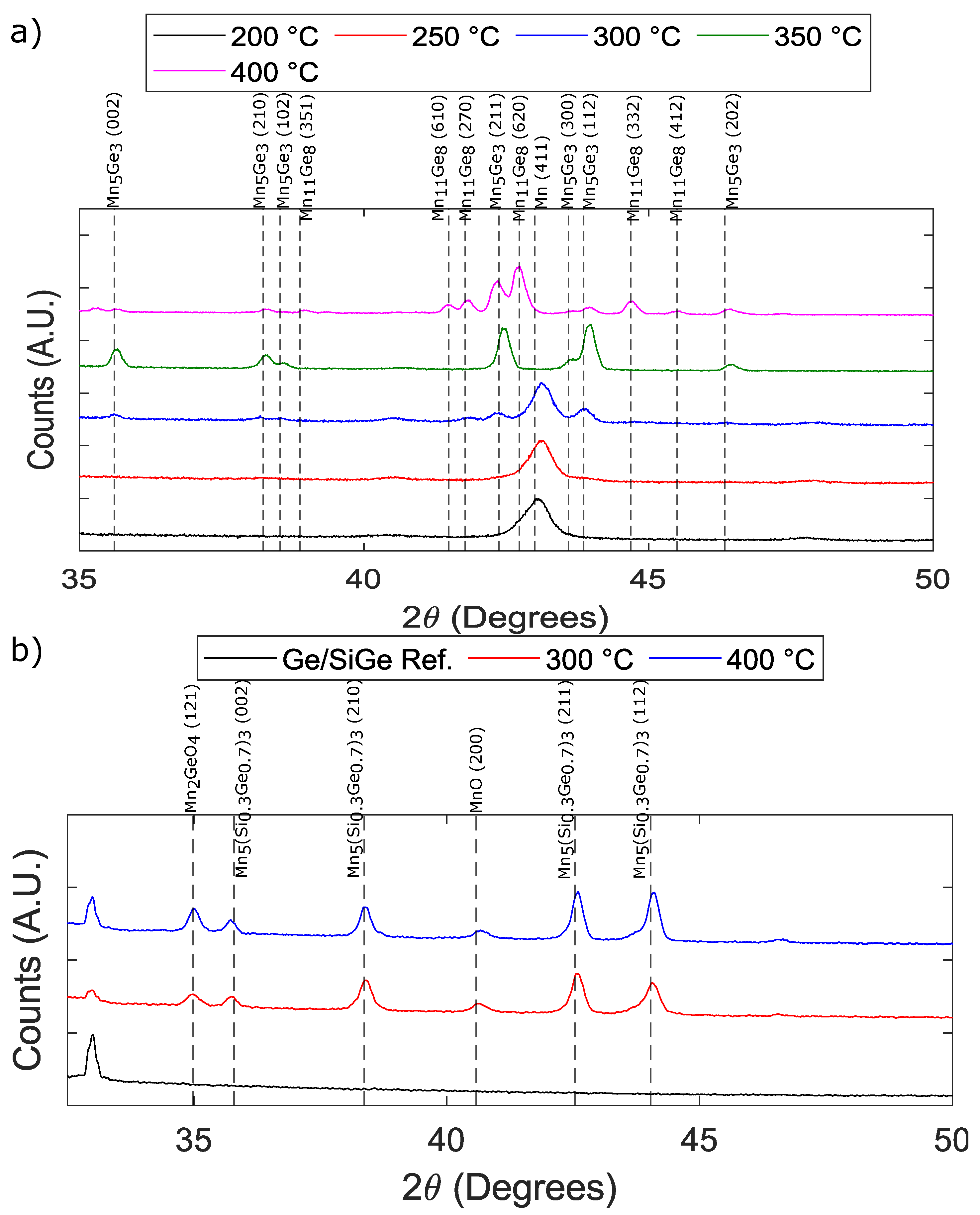
Mn thin films on bulk Ge were investigated first to verify that our process could result in phase forming before proceeding to the Ge/SiGe heterostructures. Studies have shown that formed via solid-state synthesis on (100) Ge and can occur from 250 °C up to 450 °C [27,28]. Therefore, we chose to proceed with 50 °C increments from 200 °C to 400 °C to deduce the appropriate annealing temperature for our annealing setup. X-ray diffraction (XRD) analysis of scans was performed to investigate the various phases of the Mn-Ge system formed at each of the annealing temperatures. The resulting scans and their analyses are shown in Figure 1. A detailed summary of the XRD analysis is represented in Table 1. Table 1 highlights the various phases found with corresponding , planes, lattice parameters (d-values), unit cell volume, and crystallite sizes extracted from the prominent peak of each phase at each annealing temperature. Crystallite sizes were determined using the Scherrer equation:
Here, is the crystallite size in Å, is the X-ray wavelength in Å, is the full width at half max in radians, and is the diffraction angle. The XRD system we use has a wavelength of Å.
The XRD results for Mn on bulk Ge are summarized in Figure 1a, and fitting was performed with the International Centre for Diffraction Data (ICDD) database, PDF-2 [29]. When annealed at 200 °C (black curve), the film was determined to be a Mn- phase. The Mn- phase’s characteristic feature is the peak at 43° corresponding to the (411) plane. Annealing at 200 °C resulted in a Mn- crystallite size of Å. Similar to annealing at 200 °C, annealing at 250 °C (red curve) and 300 °C (blue curve) also resulted in the Mn- phase with crystallite sizes of Å and Å, respectively. However, at 300 °C, the peak around 43° started to diminish, and smaller signatures started to appear at both higher and lower diffraction angles. These observed deviations indicate that Mn started to react with Ge to form as this is the first phase known to form [27,28]. Next, the sample annealed at 350 °C (green curve) showed the same signatures that started to appear in the 300 °C–anneal sample with higher intensities. Furthermore, the characteristic peak of the Mn- phase at 43° disappeared and was replaced by two peaks at around 42.35° and 43.73° corresponding to the (211) and (112) planes, respectively. Additionally, there were peaks at 35.46°, 38.24°, 38.38°, and 46.22° that were only prominent at 350 °C, which arose from the (002), (210), (102), and (202) planes, respectively. The peaks of the 350 °C sample fit to , confirming that indeed started to form at 300 °C. The prominent peak for was at 42.35°, by which crystallite sizes of Å, Å, and Å were extracted, respectively, at 300 °C, 350 °C, and 400 °C. By 400 °C (magenta curve), most peaks disappeared, and the new peaks fit to . A crystallite size of Å was obtained from the prominent peak at 42.73°. Based on the XRD results above, these annealing conditions can be transferred to Ge/SiGe heterostructures to form and likely within the narrower range of 300–400 °C with the most promising temperature being 350 °C.
Figure 1b shows the XRD results for the annealed Mn films on the Ge/SiGe heterostructure and a reference scan (black curve) of Ge/SiGe. The Ge/SiGe heterostructures were annealed at 300 °C (red curve) and 400 °C (blue curve). Both the 300 °C and 400 °C data are similar with only the relative heights of peaks changing between the two. The XRD peaks best fit to , , and . However, the peaks do not perfectly align with the data. We expect phases to have the form ( as our material has barriers, and this could explain the deviation from the fit. Nevertheless, XRD has detected the formation of the correct crystal structure type (, but microscopic verification is needed to confirm specifics about relative concentrations.
3.2. Scanning Transmission Electron Microscopy Analysis
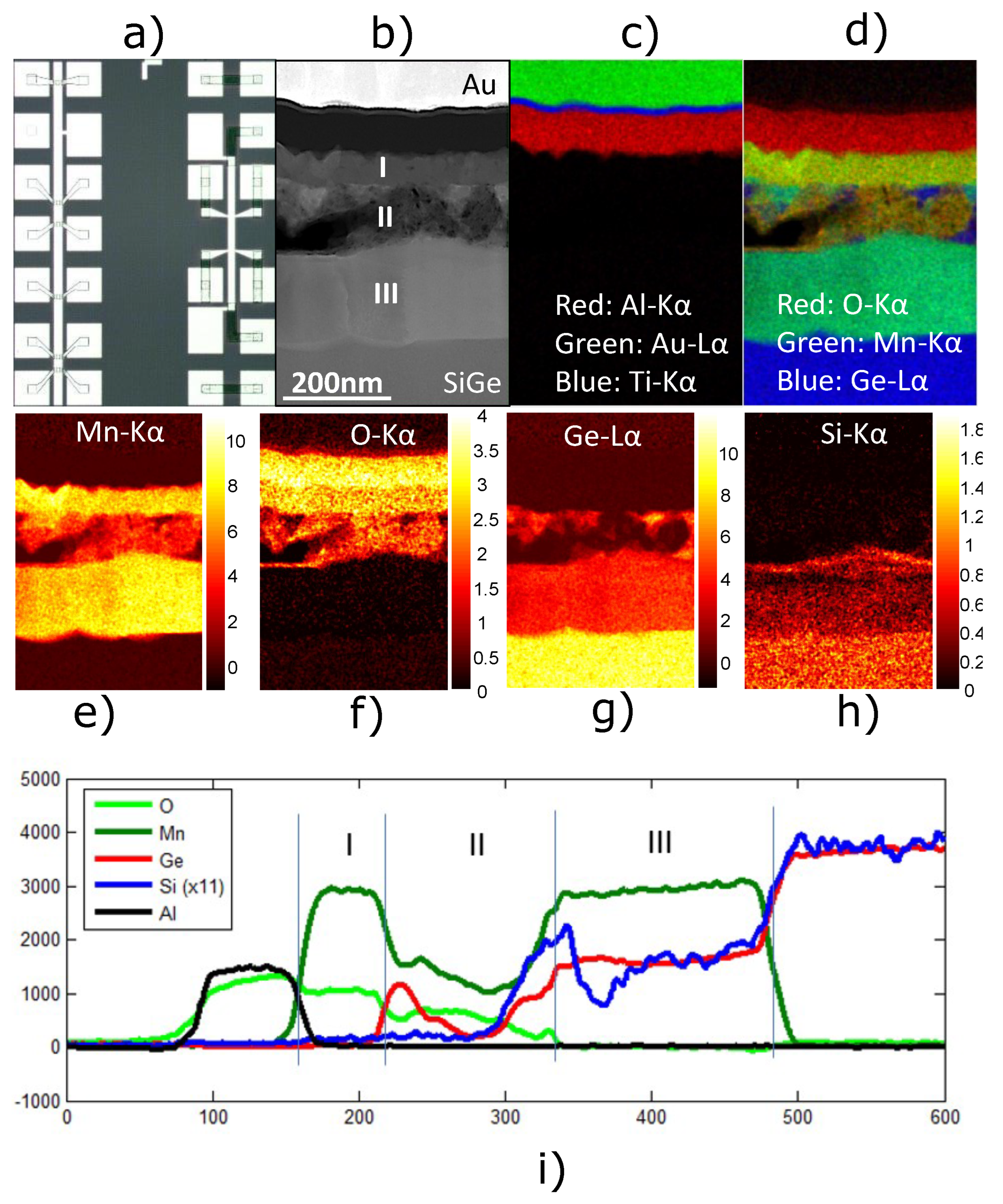
We chose 350 °C as the optimal annealing temperature for making ( contacts since it was confirmed to be the best temperature for on bulk Ge and gave a ±50 °C tolerance to the Ge/SiGe XRD results. We proceeded to make transmission line measurement (TLM) and Hall bar devices with ( contacts. An optical microscopy image in Figure 2a shows an example of the TLM (left) and Hall bar (right) devices after fabrication. The sample was used in electrical characterizations and microanalysis. Here, we discus the microanalysis results. High-resolution scanning transmission electron microscopy (HR-STEM) imaging, in combination with energy dispersive X-ray spectroscopy (EDS), was used to investigate the ( contacts in further detail. EDS provides a means to map elements in a structure by their respective K, L, and other X-ray signatures. The elements’ signatures are then represented by a false coloring in the STEM images. The STEM high-angle annular dark-field (HAADF) image in Figure 2b reveals a complex structure stack with not-well-defined boundaries. The regions labeled I, II, and III correspond to the contact structure that is of interest. The material below the region of interest is the virtual substrate. The material atop the regions of interest correspond to the Au/Ti metal contact pads and the gate oxide. The EDS data in Figure 2c verify the clear distinction between the metal/oxide region and the complex contact regions. Here, Au is represented with green, blue corresponds to Ti, and red corresponds to Al (from ). Black represents the absence of any detected signatures. Figure 2d shows an overlay of Mn, O, and Ge maps, revealing the complexity of the structure. Here, green corresponds to Mn, blue is Ge, and red is O.
Focusing on region I, the Mn ( Figure 2e) and O ( Figure 2f) elemental maps show that region I is entirely composed of Mn and O and is approximately 70 thick. This claim is supported by the absence of Ge and Si in region I, as shown in their respective elemental maps in Figure 2g,h. The Mn and O maps provide supporting evidence that the broad peak in the XRD data indeed corresponds to oxidized Mn. Furthermore, region I was determined to be polycrystalline MnO through HR-STEM HAADF imaging. Region II, like region I, contains Mn and O. However, region II also contains Ge and is approximately 116 thick. Unlike any of the other regions, region II does not have a uniform distribution of elements. Together, the Ge (Figure 2g) and Si (Figure 2h) data highlight the complexity of region II. The Si map shows only trace amounts where there are large concentrations of Ge. The Ge map shows that there are islands of Ge mostly near the region I/region II interface. Interestingly, the Mn and O distributions are nearly uniform in region II except at the areas of highest Ge concentrations and where the EDS data do not correspond to any of the elements tested (black region). This black region, most easily visualized in Figure 2d, could indicate the presence of a void since there are none of the expected elemental signatures and a lack of resolvable features in the HAADF STEM image. The Mn and Ge maps indicate a low concentration likely coming from behind the void. While voids could still occur due to the diffusion of Ge as discussed, the formation here is likely due to the complexity of the reaction that occurred. A better-quality film will form when annealed in a high-vacuum environment, and voids will be less likely to form [30,31,32,33]. Besides the islands of Ge, region II is likely a mixture of and due to its location between region I and region III, which is consistent with previous reports of solid-state syntheses of [33,34,35,36].
Region III, the largest of the three regions with a thickness of approximately 186 , appears to have the best film quality (as determined by HR-STEM) and a promising elemental map for ( contacts. The film has relatively uniform distributions of Mn, Ge, and dilute Si, as emphasized by the integrated EDS line profile in Figure 2i. Furthermore, the Si line is magnified such that when Si and Ge counts are equal, it represents the relative concentration of the barrier . The region II/III interface is where the Ge/SiGe heterostructure starts. While it is clear that Mn is being driven into the heterostructure, the presence of Ge in region II indicates that Ge has left the heterostructure, thus making the heterostructure more Si rich.
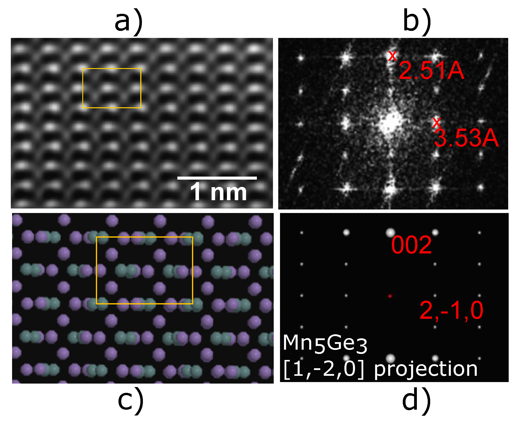
To further investigate the film, HR-STEM HAADF imaging along with its fast Fourier transform (FFT) pattern was used to determine the exact phase of (. The STEM HAADF image of ( in Figure 3a, along with its FFT pattern in Figure 3b, is in excellent agreement with the projected structure (Figure 3c) and simulated selected area electron diffraction (SAED) pattern (Figure 3d) corresponding to the hexagonal crystal structure of . The SAED pattern is calculated using reciprocal lattice and associated electron structure factors under the kinematical approximation [37]. The geometry of the pattern (or relative positions of the reciprocal lattice) is important in this context, and fits exactly the FFT pattern in [1, −2, 0], confirming the phase. Since the starting material consisted of mostly layers, except for the Ge quantum well and Si cap, it is likely that the relative concentrations of Si and Ge remained near their original concentrations such that the film is (. The EDS line scan, calibrated to the virtual substrate beyond region III, is consistent with this claim. The XRD data showed a fit with or (, and this could be due to the larger concentration of Si at the interface of region II and region III. Nevertheless, our data revealed the correct phase of ( to make a p-type ferromagnetic contact for Ge/SiGe heterostructure field-effect transistors (HFETs).
3.3. Electrical Characterization
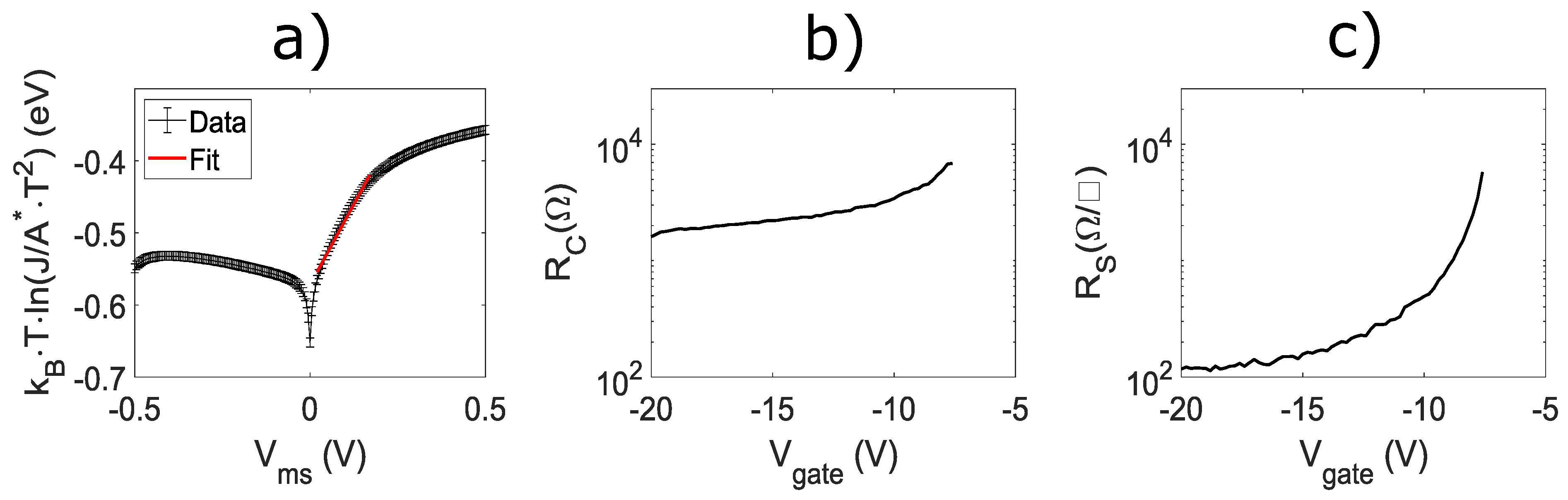
With the confirmation of solid-state-reaction-formed -based contacts on undoped Ge/SiGe heterostructures, we present the electrical properties of the contacts from Schottky diodes, TLM, and Hall bar measurements. Since it can be difficult to analyze Schottky contacts on quantum well heterostructures, our Schottky diodes were fabricated on n-type (100) Ge, with a resistivity range of 1–10 cm, to estimate the Schottky barrier height of /Ge. /n-Ge Schottky diodes serve as a good analogue for estimating the barrier height for /Ge in our Ge/SiGe heterostructure devices. Ideally, there would be an increase in barrier height due to the compressive strain of the Ge quantum well moving both the conduction and valence band edges farther apart [38,39]. However, Ge is widely known to pin the Fermi levels of most metals very close to the valence band edge, thus nullifying any effects due to strain in the case of hole transport. The lack of strain affecting barrier heights due to Fermi level pinning has been shown in the case of n-type SiGe [40]. While /n-Ge is not a direct replacement for the /stained-Ge quantum well, it does provide the best estimate available. A direct measurement for our system would require contact only of the quantum well with in an isolated fashion, which is extremely difficult, especially given its relatively small thickness. To fabricate the /Ge Schottky diodes, Mn films on Ge were etched back into circular contacts and then annealed to form . The Schottky diodes were made with a radius of 200 . The /Ge Schottky diodes were characterized using current density–voltage analysis at room temperature. The current density–voltage data are represented in Figure 4a. The Schottky barrier height is extracted from the following relation:
Here, is the voltage corresponding to the thermal energy in , is the Richardson constant, T is the temperature, J is the current density, V is the voltage, n is a nonideality factor, and is the Schottky barrier height. The red line in Figure 4d is the fit line where a Schottky barrier height, with respect to the Ge conduction band, of 0.57(1) is obtained. The fit assumes 44.5(105) // and 300 . Therefore, has a Schottky barrier height of 0.10(1) with respect to the Ge valence band. The assumptions made and the obtained Schottky barrier height are consistent with other studies [1,2,25,32,41].
While the Schottky diode on bulk n-type Ge gives an estimate of the /Ge barrier height for the heterostructure, it does not provide a full scope of the contact’s electrical characteristics. Devices made with Ge/SiGe will be enhancement-mode heterostructure field-effect transistors (HFETs), whose characteristics will be dependent on applied gate voltages. Furthermore, the material was grown such that there was high-quality transport at cryogenic temperatures. Therefore, we fabricated TLM and Hall bar devices (as previously described [13], except with surface preparation, as described in this manuscript) to measure the contacts’ properties under these conditions. TLM and Hall measurements were performed using four-terminal, low-frequency lock-in techniques at a temperature of 4 using a liquid helium cryostat. A 100 sinusoidal excitation was sourced from a lock-in for both the TLM and Hall measurements. For Hall measurements, the magnetic field was swept from −0.5 to 0.5 T.
TLM devices provide a means to extract the contact and gate-induced 2D hole gas (2DHG) sheet resistances of materials. Our TLM devices (left device in Figure 2a) were made with 25 × 50 –based contacts with separations (channel lengths) of 50 , 100 , 325 , 400 , and 675 . A 50 –wide gate that overlaps with all the contacts provides a means to capacitively induce 2DHG. A more negative gate voltage increases the 2DHG density and decreases the 2DHG sheet resistance. Contact resistance was obtained from the TLM device using two different methods, each using the TLM equation, assuming that the contact resistance is much larger than the resistance of the metal pads:
Here, is the total measured resistance, is the 2DHG sheet resistance, is the ratio of the channel length to the channel width, and is the contact resistance. The first method used is the standard approach, where the total resistance is measured as a function channel length, a linear fit is performed, and the contact resistance is half the y-intercept of the linear fit. The 2DHG sheet resistance is then extracted by multiplying the fit’s slope by the channel width. The extracted contact resistance and 2DHG sheet resistance, as a function of gate voltage, are shown in Figure 4b,c, respectively. A contact resistance in the order of 1 across the measured voltage range was obtained. Interestingly, the 2DHG sheet resistance saturates at gate voltages more negative than −15 V, while the contact resistance has a linear dependence on gate voltage after the saturation of the device. The gate voltage dependence past saturation can be explained by the gate’s overlap with the -based contact. Although the saturation of holes has been achieved in the channel of the device, the electric field from the gate lowers the injection barrier. Thus, as the gate voltage is further increased past saturation, there is still a measured reduction in the contact resistance [42,43,44], while the 2DHG sheet resistance is no longer sensitive to the gate voltage. If there was no Schottky barrier at the /Ge interface in the Ge/SiGe HFET device, then both the 2DHG sheet resistance and the contact resistance would saturate, indicating an ohmic contact. An ohmic contact has little to no barrier such that charge transport is unaffected by any additional band bending at the metal/semiconductor interface. However, a Schottky barrier would be affected by further band bending. Either image-force lowering of the barrier height occurs or the barrier thickness is reduced. In either case, the result is an increase in the supply of carriers from an effectively reduced contact resistance [45].
To verify the behavior of the contact resistance past saturation, contact resistance was determined using a second method. The second method used involves subtracting off the sheet resistance component from the total resistance for each resistance measurement and dividing by 2 (for the two current contacts). This was made possible because the sheet resistance was obtained through a four-terminal measurement. The contact resistance obtained by the second method was then averaged across three different devices. The second method data (black) are shown in Figure 5a, where the error bars correspond to the standard deviation. The contact resistance obtained by the first method is overlaid in red. As expected, the two methods for extracting contact resistance were consistent with one another. The Hall density versus gate voltage data in Figure 5b show that a saturation density of 8 × 1011 cm−2 is obtained at a gate voltage of . The mobility versus density data in Figure 5c show that a peak mobility of 2.1 × 105 cm2V−1s−1 is achieved at a density of 8 × 1011 cm−2. The transport data using -based contact are consistent with what was previously observed in the same Ge/SiGe heterostructures with PtSiGe-based contacts [13]. The saturation of Hall density with a higher gate voltage is characteristic of Ge/SiGe quantum well systems and is consistent with the saturation of the 2DHG sheet resistance. This further supports that the reduction in contact resistance is due to the capacitive coupling of the gate to the Schottky barrier.
4. Conclusions
We investigated -based contacts created via solid-state synthesis on a shallow Ge/SiGe quantum well heterostructure. XRD was used to determine the proper annealing temperature for the phase formation, while STEM HAADF and its FFT image were used to verify the formation of the target Mn-Ge phase. Although our solid-state synthesis could be improved to eliminate the unwanted oxides ( and ) observed, the -based contacts were observed to work well as p-type contacts for Ge/SiGe HFETs even at cryogenic temperatures. Our electrical characterization results were consistent with what is expected for contacts and other p-type contacts on Ge/SiGe.
Our demonstration of the solid-state synthesis of -based contacts for a shallow Ge/SiGe quantum well heterostructure provides a clear path towards demonstrating spin transport in Ge 2DHG systems similar to what was done in Si 2DEG systems [46] and Ge nanowires [1,2]. The evidence of Schottky barrier lowering, shown from a decreasing contact resistance past saturation, is promising for efficient spin injection and its gate tunability [47]. Future studies should include studying the magnetic properties of ( (formed after the removal of the top barrier and quantum well) and spin transport in the Ge/SiGe heterostructure.
Author Contributions
Conceptualization, T.A.H.-D. and T.-M.L.; methodology, T.A.H.-D. and T.-M.L.; software, T.A.H.-D.; validation, T.A.H.-D., S.J.A., P.L. and T.-M.L.; formal analysis, T.A.H.-D. and P.L.; investigation, T.A.H.-D.; resources, T.-M.L.; data curation, T.A.H.-D., S.J.A. and P.L.; writing—original draft preparation, T.A.H.-D.; writing—review and editing, T.A.H.-D., S.J.A., P.L. and T.-M.L.; visualization, T.A.H.-D.; supervision, T.-M.L.; project administration, T.-M.L.; funding acquisition, T.-M.L. All authors have read and agreed to the published version of the manuscript.
Funding
This research received no external funding.
Data Availability Statement
Data will be available upon request.
Acknowledgments
This research was primarily supported by the Laboratory Directed Research and Development Program at Sandia National Laboratories (SNL). This work was performed, in part, at the Center for Integrated Nanotechnologies, an Office of Science user facility operated for the U.S. Department of Energy (DOE) Office of Science. SNL is a multimission laboratory managed and operated by National Technology and Engineering Solutions of Sandia LLC, a wholly owned subsidiary of Honeywell International Inc. for the U.S. DOE National Nuclear Security Administration under contract number DE-NA0003525. This paper describes objective technical results and analysis. Any subjective views or opinions that might be expressed in the paper do not necessarily represent the views of the U.S. DOE or the United States government. The data that support the findings of this study are available from the corresponding author upon reasonable request.
Conflicts of Interest
The authors declare no conflicts of interest.
References
- Tang, J.; Wang, C.Y.; Hung, M.H.; Jiang, X.; Chang, L.T.; He, L.; Liu, P.H.; Yang, H.J.; Tuan, H.Y.; Chen, L.J.; et al. Ferromagnetic germanide in Ge nanowire transistors for spintronics application. ACS Nano 2012, 6, 5710–5717. [Google Scholar] [CrossRef] [PubMed]
- Tang, J.; Wang, C.Y.; Chang, L.T.; Fan, Y.; Nie, T.; Chan, M.; Jiang, W.; Chen, Y.T.; Yang, H.J.; Tuan, H.Y.; et al. Electrical spin injection and detection in Mn5Ge3/Ge/Mn5Ge3 nanowire transistors. Nano Lett. 2013, 13, 4036–4043. [Google Scholar] [CrossRef] [PubMed]
- Morrison, C.; Wiśniewski, P.; Rhead, S.; Foronda, J.; Leadley, D.R.; Myronov, M. Observation of Rashba zero-field spin splitting in a strained germanium 2D hole gas. Appl. Phys. Lett. 2014, 105, 182401. [Google Scholar] [CrossRef]
- Hardy, W.J.; Harris, C.T.; Su, Y.H.; Chuang, Y.; Moussa, J.; Maurer, L.N.; Li, J.Y.; Lu, T.M.; Luhman, D.R. Single and double hole quantum dots in strained Ge/SiGe quantum wells. Nanotechnology 2019, 30, 215202. [Google Scholar] [CrossRef]
- Sammak, A.; Sabbagh, D.; Hendrickx, N.W.; Lodari, M.; Paquelet Wuetz, B.; Tosato, A.; Yeoh, L.; Bollani, M.; Virgilio, M.; Schubert, M.A.; et al. Shallow and undoped germanium quantum wells: A playground for spin and hybrid quantum technology. Adv. Funct. Mater. 2019, 29, 1807613. [Google Scholar] [CrossRef]
- Hendrickx, N.; Lawrie, W.; Petit, L.; Sammak, A.; Scappucci, G.; Veldhorst, M. A single-hole spin qubit. Nat. Commun. 2020, 11, 3478. [Google Scholar] [CrossRef] [PubMed]
- Hendrickx, N.; Franke, D.; Sammak, A.; Scappucci, G.; Veldhorst, M. Fast two-qubit logic with holes in germanium. Nature 2020, 577, 487–491. [Google Scholar] [CrossRef] [PubMed]
- Hendrickx, N.W.; Lawrie, W.I.; Russ, M.; van Riggelen, F.; de Snoo, S.L.; Schouten, R.N.; Sammak, A.; Scappucci, G.; Veldhorst, M. A four-qubit germanium quantum processor. Nature 2021, 591, 580–585. [Google Scholar] [CrossRef]
- Van Riggelen, F.; Hendrickx, N.; Lawrie, W.; Russ, M.; Sammak, A.; Scappucci, G.; Veldhorst, M. A two-dimensional array of single-hole quantum dots. Appl. Phys. Lett. 2021, 118, 044002. [Google Scholar] [CrossRef]
- Miller, A.J.; Hardy, W.J.; Luhman, D.R.; Brickson, M.; Baczewski, A.; Liu, C.Y.; Li, J.Y.; Lilly, M.P.; Lu, T.M. Effective out-of-plane g factor in strained-Ge/SiGe quantum dots. Phys. Rev. B 2022, 106, L121402. [Google Scholar] [CrossRef]
- Lodari, M.; Kong, O.; Rendell, M.; Tosato, A.; Sammak, A.; Veldhorst, M.; Hamilton, A.; Scappucci, G. Lightly strained germanium quantum wells with hole mobility exceeding one million. Appl. Phys. Lett. 2022, 120, 122104. [Google Scholar] [CrossRef]
- Kong, Z.; Li, Z.; Cao, G.; Su, J.; Zhang, Y.; Liu, J.; Liu, J.; Ren, Y.; Li, H.; Wei, L.; et al. Undoped Strained Ge Quantum Well with Ultrahigh Mobility of Two Million. ACS Appl. Mater. Interfaces 2023, 15, 28799–28805. [Google Scholar] [CrossRef] [PubMed]
- Hutchins-Delgado, T.A.; Miller, A.J.; Scott, R.; Lu, P.; Luhman, D.R.; Lu, T.M. Characterization of Shallow, Undoped Ge/SiGe Quantum Wells Commercially Grown on 8-in. (100) Si Wafers. ACS Appl. Electron. Mater. 2022, 4, 4482–4489. [Google Scholar] [CrossRef]
- Chou, C.T.; Jacobson, N.T.; Moussa, J.E.; Baczewski, A.D.; Chuang, Y.; Liu, C.Y.; Li, J.Y.; Lu, T.M. Weak anti-localization of two-dimensional holes in germanium beyond the diffusive regime. Nanoscale 2018, 10, 20559–20564. [Google Scholar] [CrossRef]
- Virgilio, M.; Grosso, G. Optical spin orientation in strained Ge/SiGe quantum wells: A tight-binding approach. Phys. Rev. B 2009, 80, 205309. [Google Scholar] [CrossRef]
- Pezzoli, F.; Bottegoni, F.; Trivedi, D.; Ciccacci, F.; Giorgioni, A.; Li, P.; Cecchi, S.; Grilli, E.; Song, Y.; Guzzi, M.; et al. Optical spin injection and spin lifetime in Ge heterostructures. Phys. Rev. Lett. 2012, 108, 156603. [Google Scholar] [CrossRef]
- Schmidt, G.; Ferrand, D.; Molenkamp, L.; Filip, A.; Van Wees, B. Fundamental obstacle for electrical spin injection from a ferromagnetic metal into a diffusive semiconductor. Phys. Rev. B 2000, 62, R4790. [Google Scholar] [CrossRef]
- Fert, A.; Jaffres, H. Conditions for efficient spin injection from a ferromagnetic metal into a semiconductor. Phys. Rev. B 2001, 64, 184420. [Google Scholar] [CrossRef]
- Jeon, K.R.; Min, B.C.; Jo, Y.H.; Lee, H.S.; Shin, I.J.; Park, C.Y.; Park, S.Y.; Shin, S.C. Electrical spin injection and accumulation in CoFe/MgO/Ge contacts at room temperature. Phys. Rev. B 2011, 84, 165315. [Google Scholar] [CrossRef]
- Zhou, Y.; Han, W.; Chang, L.T.; Xiu, F.; Wang, M.; Oehme, M.; Fischer, I.A.; Schulze, J.; Kawakami, R.K.; Wang, K.L. Electrical spin injection and transport in germanium. Phys. Rev. B 2011, 84, 125323. [Google Scholar] [CrossRef]
- Iba, S.; Saito, H.; Spiesser, A.; Watanabe, S.; Jansen, R.; Yuasa, S.; Ando, K. Spin accumulation and spin lifetime in p-type germanium at room temperature. Appl. Phys. Express 2012, 5, 053004. [Google Scholar] [CrossRef]
- Jain, A.; Vergnaud, C.; Peiro, J.; Le Breton, J.; Prestat, E.; Louahadj, L.; Portemont, C.; Ducruet, C.; Baltz, V.; Marty, A.; et al. Electrical and thermal spin accumulation in germanium. Appl. Phys. Lett. 2012, 101, 022402. [Google Scholar] [CrossRef]
- Sharma, S.; Spiesser, A.; Dash, S.P.; Iba, S.; Watanabe, S.; Van Wees, B.; Saito, H.; Yuasa, S.; Jansen, R. Anomalous scaling of spin accumulation in ferromagnetic tunnel devices with silicon and germanium. Phys. Rev. B 2014, 89, 075301. [Google Scholar] [CrossRef]
- Picozzi, S.; Continenza, A.; Freeman, A. First-principles characterization of ferromagnetic Mn5Ge3 for spintronic applications. Phys. Rev. B 2004, 70, 235205. [Google Scholar] [CrossRef]
- Spiesser, A.; Saito, H.; Jansen, R.; Yuasa, S.; Ando, K. Large spin accumulation voltages in epitaxial Mn5Ge3 contacts on Ge without an oxide tunnel barrier. Phys. Rev. B 2014, 90, 205213. [Google Scholar] [CrossRef]
- Ponath, P.; Posadas, A.; Demkov, A. Ge (001) surface cleaning methods for device integration. Appl. Phys. Rev. 2017, 4, 021308. [Google Scholar] [CrossRef]
- Wittmer, M.; Nicolet, M.A.; Mayer, J. The first phase to nucleate in planar transition metal-germanium interfaces. Thin Solid Films 1977, 42, 51–59. [Google Scholar] [CrossRef]
- Gokhale, A.; Abbaschian, R. The Ge-Mn (germanium-manganese) system. J. Phase Equilibria 1990, 11, 460–468. [Google Scholar] [CrossRef]
- Gates-Rector, S.; Blanton, T. The powder diffraction file: A quality materials characterization database. Powder Diffr. 2019, 34, 352–360. [Google Scholar] [CrossRef]
- Olive-Mendez, S.; Spiesser, A.; Michez, L.; Le Thanh, V.; Glachant, A.; Derrien, J.; Devillers, T.; Barski, A.; Jamet, M. Epitaxial growth of Mn5Ge3/Ge (111) heterostructures for spin injection. Thin Solid Films 2008, 517, 191–196. [Google Scholar] [CrossRef]
- Spiesser, A.; Olive-Mendez, S.; Dau, M.T.; Michez, L.; Watanabe, A.; Le Thanh, V.; Glachant, A.; Derrien, J.; Barski, A.; Jamet, M. Effect of thickness on structural and magnetic properties of Mn5Ge3 films grown on Ge (111) by solid phase epitaxy. Thin Solid Films 2010, 518, S113–S117. [Google Scholar] [CrossRef]
- Nishimura, T.; Nakatsuka, O.; Akimoto, S.; Takeuchi, W.; Zaima, S. Crystalline orientation dependence of electrical properties of Mn Germanide/Ge (1 1 1) and (0 0 1) Schottky contacts. Microelectron. Eng. 2011, 88, 605–609. [Google Scholar] [CrossRef]
- Xie, Y.; Yuan, Y.; Wang, M.; Xu, C.; Hübner, R.; Grenzer, J.; Zeng, Y.J.; Helm, M.; Zhou, S.; Prucnal, S. Epitaxial Mn5Ge3 (100) layer on Ge (100) substrates obtained by flash lamp annealing. Appl. Phys. Lett. 2018, 113, 222401. [Google Scholar] [CrossRef]
- Abbes, O.; Portavoce, A.; Le Thanh, V.; Girardeaux, C.; Michez, L. Phase formation during Mn thin film reaction with Ge: Self-aligned germanide process for spintronics. Appl. Phys. Lett. 2013, 103, 172405. [Google Scholar] [CrossRef]
- Myagkov, V.; Zhigalov, V.; Matsynin, A.; Bykova, L.; Mikhlin, Y.L.; Bondarenko, G.; Patrin, G.; Yurkin, G.Y. Formation of ferromagnetic germanides by solid-state reactions in 20 Ge/80 Mn films. Thin Solid Films 2014, 552, 86–91. [Google Scholar] [CrossRef]
- Myagkov, V.; Bykova, L.; Matsynin, A.; Volochaev, M.; Zhigalov, V.; Tambasov, I.; Mikhlin, Y.L.; Velikanov, D.; Bondarenko, G. Solid state synthesis of Mn5Ge3 in Ge/Ag/Mn trilayers: Structural and magnetic studies. J. Solid State Chem. 2017, 246, 379–387. [Google Scholar] [CrossRef]
- Cowley, J.M. Diffraction Physics; Elsevier: Amsterdam, The Netherlands, 1995. [Google Scholar]
- Adachi, S. Properties of Semiconductor Alloys: Group-IV, III-V and II-VI Semiconductors; John Wiley & Sons: Hoboken, NJ, USA, 2009. [Google Scholar]
- Chuang, S.L. Physics of Photonic Devices; John Wiley & Sons: Hoboken, NJ, USA, 2012. [Google Scholar]
- Mamor, M.; Nur, O.; Karlsteen, M.; Willander, M.; Auret, F. Fermi-level pinning and Schottky barrier heights on epitaxially grown fully strained and partially relaxed n-type Si1−x Gex layers. J. Appl. Phys. 1999, 86, 6890–6894. [Google Scholar] [CrossRef]
- Sellai, A.; Mesli, A.; Petit, M.; Le Thanh, V.; Taylor, D.; Henini, M. Barrier height and interface characteristics of Au/Mn5Ge3/Ge (1 1 1) Schottky contacts for spin injection. Semicond. Sci. Technol. 2012, 27, 035014. [Google Scholar] [CrossRef]
- Lepselter, M.; Sze, S. SB-IGFET: An insulated-gate field-effect transistor using Schottky barrier contacts for source and drain. Proc. IEEE 1968, 56, 1400–1402. [Google Scholar] [CrossRef]
- Snyder, J.P.; Helms, C.; Nishi, Y. Experimental investigation of a PtSi source and drain field emission transistor. Appl. Phys. Lett. 1995, 67, 1420–1422. [Google Scholar] [CrossRef]
- Li, R.; Yao, H.; Lee, S.; Chi, D.; Yu, M.; Lo, G.; Kwong, D. Metal-germanide Schottky source/drain transistor on germanium substrate for future CMOS technology. Thin Solid Films 2006, 504, 28–31. [Google Scholar] [CrossRef]
- Sze, S.M.; Li, Y.; Ng, K.K. Physics of Semiconductor Devices; John Wiley & Sons: Hoboken, NJ, USA, 2021. [Google Scholar]
- Chang, L.T.; Fischer, I.A.; Tang, J.; Wang, C.Y.; Yu, G.; Fan, Y.; Murata, K.; Nie, T.; Oehme, M.; Schulze, J.; et al. Electrical detection of spin transport in Si two-dimensional electron gas systems. Nanotechnology 2016, 27, 365701. [Google Scholar] [CrossRef] [PubMed]
- Dankert, A.; Dulal, R.S.; Dash, S.P. Efficient spin injection into silicon and the role of the Schottky barrier. Sci. Rep. 2013, 3, 3196. [Google Scholar] [CrossRef] [PubMed]
Figure 1.
Summary of XRD scans. (a) XRD scans for thermal evaporated Mn thin films on (100) Ge substrates and annealed at 200 °C (black), 250 °C (red), 300 °C (blue), 350 °C (green), and 400 °C (magenta). The black vertical lines correspond to ICDD peak locations for and . (b) XRD scans for thermal evaporated Mn thin films on quantum well heterostructures and annealed at 300 °C (red) and 400 °C (blue). The reference scan is shown in black. The vertical lines correspond to ICDD peak locations for ( and various oxides: and .

Figure 2.
Cross-sectional STEM and EDS analysis of -based contacts for Ge/SiGe H-FET devices. (a) Optical microscope image TLM (left) and Hall bar (right) devices. (b) HAADF STEM image of the -based contact material stack. (c) Combined EDS map of the Au (red)/Ti (blue) gate metal and (Al-red) gate dielectric above the -based contact. (d) Combined EDS mapping of O (red), Mn (green), and Ge (blue). (e) EDS map of Mn, (f) EDS map of O, (g) EDS map of Ge, (h) EDS mapping of Si, and (i) integrated EDS line profile with signatures of O (light green), Mn (dark green), Ge (red), Si (blue), and Al (black).

Figure 3.
STEM HAADF analysis of -based contact. (a) HR-STEM HAADF of region III. (b) FFT of the STEM HAADF image. (c) Crystal structure of . (d) Simulated SAED pattern of in the [1, −2, 0] projection.
Figure 3.
STEM HAADF analysis of -based contact. (a) HR-STEM HAADF of region III. (b) FFT of the STEM HAADF image. (c) Crystal structure of . (d) Simulated SAED pattern of in the [1, −2, 0] projection.

Figure 4.
Electrical characterization of contacts. (a) /n-type (100) Ge Schottky diode. (b) Contact resistance for TLM H-FET device. (c) Sheet resistance for TLM H-FET device.
Figure 4.
Electrical characterization of contacts. (a) /n-type (100) Ge Schottky diode. (b) Contact resistance for TLM H-FET device. (c) Sheet resistance for TLM H-FET device.

Figure 5.
Transport characterization with contacts. (a) Comparison of contact resistance obtained via Hall data (black) and TLM (red). (b) Hall density vs. gate voltage. (c) Mobility vs. density.
Figure 5.
Transport characterization with contacts. (a) Comparison of contact resistance obtained via Hall data (black) and TLM (red). (b) Hall density vs. gate voltage. (c) Mobility vs. density.


Table 1.
Table summary of X-ray diffraction analysis.
| Phase | 2 | Plane | d-Value | Unit Cell Volume | Crystallite Size | Crystallite Size | Crystallite Size | Crystallite Size | Crystallite Size |
|---|---|---|---|---|---|---|---|---|---|
| (h k l) | (Å) | (Å3) | (200 °C) | (250 °C) | (300 °C) | (350 °C) | (400 °C) | ||
| Mn- | ° | 4 1 1 | 2.201 | 707.85 | Å | Å | Å | - | - |
| MnO | 40.55° | 2 0 0 | 2.223 | 87.88 | - | - | Å | - | Å |
| 34.74° | 1 2 1 | 2.580 | 337.59 | - | - | Å | - | Å | |
| 35.46° | 0 0 2 | 2.530 | 226.114 | - | - | - | - | - | |
| 38.24° | 2 1 0 | 2.352 | 226.114 | - | - | - | - | - | |
| 38.38° | 1 0 2 | 2.343 | 226.114 | - | - | - | - | - | |
| 42.35° | 2 1 1 | 2.132 | 226.114 | - | - | Å | Å | Å | |
| 43.61° | 3 0 0 | 2.074 | 226.114 | - | - | - | - | - | |
| 43.73° | 1 1 2 | 2.066 | 226.114 | - | - | - | - | - | |
| 46.22° | 2 0 2 | 1.963 | 226.114 | - | - | - | - | - | |
| 35.80° | 0 0 2 | 2.487 | 218.45 | - | - | - | - | - | |
| 38.37° | 2 1 0 | 2.331 | 218.45 | - | - | - | - | - | |
| 42.53° | 2 1 1 | 2.111 | 218.45 | - | - | Å | - | Å | |
| 44.03° | 1 1 2 | 2.039 | 218.45 | - | - | - | - | - | |
| 39.32° | 3 5 1 | 2.290 | 1055.77 | - | - | - | - | - | |
| 41.49° | 6 1 0 | 2.175 | 1055.77 | - | - | - | - | - | |
| 42.26° | 2 7 0 | 2.137 | 1055.77 | - | - | - | - | - | |
| 42.73° | 6 2 0 | 2.115 | 1055.77 | - | - | - | - | Å | |
| 44.69° | 3 3 2 | 2.026 | 1055.77 | - | - | - | - | - | |
| 45.50° | 4 1 2 | 1.992 | 1055.77 | - | - | - | - | - |
Disclaimer/Publisher’s Note: The statements, opinions and data contained in all publications are solely those of the individual author(s) and contributor(s) and not of MDPI and/or the editor(s). MDPI and/or the editor(s) disclaim responsibility for any injury to people or property resulting from any ideas, methods, instructions or products referred to in the content. |
© 2024 by the authors. Licensee MDPI, Basel, Switzerland. This article is an open access article distributed under the terms and conditions of the Creative Commons Attribution (CC BY) license (https://creativecommons.org/licenses/by/4.0/).
Share and Cite
MDPI and ACS Style
Hutchins-Delgado, T.A.; Addamane, S.J.; Lu, P.; Lu, T.-M. Characterization of Mn5Ge3 Contacts on a Shallow Ge/SiGe Heterostructure. Nanomaterials 2024, 14, 539. https://doi.org/10.3390/nano14060539
AMA Style
Hutchins-Delgado TA, Addamane SJ, Lu P, Lu T-M. Characterization of Mn5Ge3 Contacts on a Shallow Ge/SiGe Heterostructure. Nanomaterials. 2024; 14(6):539. https://doi.org/10.3390/nano14060539
Chicago/Turabian StyleHutchins-Delgado, Troy A., Sadhvikas J. Addamane, Ping Lu, and Tzu-Ming Lu. 2024. "Characterization of Mn5Ge3 Contacts on a Shallow Ge/SiGe Heterostructure" Nanomaterials 14, no. 6: 539. https://doi.org/10.3390/nano14060539
Note that from the first issue of 2016, this journal uses article numbers instead of page numbers. See further details here.