
Photoelectric Properties of GaS1−xSex (0 ≤ x ≤ 1) Layered Crystals
by
 and
and
Yu-Tai Shih
1,
Der-Yuh Lin
2,*,
Bo-Chang Tseng
3,
Ting-Chen Huang
1,
Yee-Mou Kao
1,
Ming-Cheng Kao
4 and
Sheng-Beng Hwang
5 1
Department of Physics, National Changhua University of Education, Changhua 500207, Taiwan
2
Department of Electronic Engineering, National Changhua University of Education, Changhua 500208, Taiwan
3
Graduate Institute of Photonics, National Changhua University of Education, Changhua 500207, Taiwan
4
Department of Information and Communication Engineering, Chaoyang University of Technology, Taichung 413310, Taiwan
5
Department of Electronic Engineering, Chienkuo Technology University, Changhua 500020, Taiwan
*
Author to whom correspondence should be addressed.
Nanomaterials 2024, 14(8), 701; https://doi.org/10.3390/nano14080701
Submission received: 5 March 2024
/
Revised: 14 April 2024
/
Accepted: 15 April 2024
/
Published: 18 April 2024
(This article belongs to the Special Issue 2D Materials and van der Waals Heterostructures for Optoelectronic Devices)
Abstract
:In this study, the photoelectric properties of a complete series of GaS1−xSex (0 ≤ x ≤ 1) layered crystals are investigated. The photoconductivity spectra indicate a decreasing bandgap of GaS1−xSex as the Se composition x increases. Time-resolved photocurrent measurements reveal a significant improvement in the response of GaS1−xSex to light with increasing x. Frequency-dependent photocurrent measurements demonstrate that both pure GaS crystals and GaS1−xSex ternary alloy crystals exhibit a rapid decrease in photocurrents with increasing illumination frequency. Crystals with lower x exhibit a faster decrease in photocurrent. However, pure GaSe crystal maintains its photocurrent significantly even at high frequencies. Measurements for laser-power-dependent photoresponsivity and bias-voltage-dependent photoresponsivity also indicate an increase in the photoresponsivity of GaS1−xSex as x increases. Overall, the photoresponsive performance of GaS1−xSex is enhanced with increasing x, and pure GaSe exhibits the best performance. This result contradicts the findings of previous reports. Additionally, the inverse trends between bandgap and photoresponsivity with increasing x suggest that GaS1−xSex-based photodetectors could potentially offer a high response and wavelength-selectivity for UV and visible light detection. Thus, this work provides novel insights into the photoelectric characteristics of GaS1−xSex layered crystals and highlights their potential for optoelectronic applications.
1. Introduction
GaS and GaSe are layered crystals belonging to the IIIA-VIA compound family and are classified as post-transition metal monochalcogenides [1,2,3]. The room-temperature bandgaps of GaS and GaSe reported in the literature range from 2.46 eV to 2.83 eV [4,5,6,7,8,9,10] and 1.95 eV to 2.03 eV [7,8,9,10,11,12,13,14], respectively. Therefore, GaS and GaSe have the potential to be used in the fabrication of optoelectronic devices for applications in the red and blue visible light regions. For instance, GaS has been described as a promising semiconductor for use in near-blue-light-emitting devices [15]. On the other hand, GaSe is also promising for optoelectronic devices in the visible range [16].
GaS and GaSe crystals can be fabricated into atomically thin, two-dimensional (2D) layered structures [17,18,19,20,21,22,23] due to the weak van der Waals forces between their adjacent monolayers [1,24]. Recent research has highlighted the intriguing properties exhibited by these 2D layered structures. For example, the photodetectors based on 2D layered structures of GaSe showed high performance of photoresponse in the UV and visible regions [19,22,25,26]. The GaSe thin film consisting of a few layers displayed a significant absorption coefficient [20]. Furthermore, strong second-harmonic generation was found in atomic layered GaSe [27,28]. On the other hand, the photodetectors based on 2D nanoflakes of GaS demonstrated a relevant UV-selective photoresponse [23]. The superior nonlinear optical activities were also found in the 2D layered structures of GaS [29]. The unique properties and high performance position 2D layered structures of GaS and GaSe as promising materials for applications in next-generation optoelectronics and electronics.
To engineer the properties of GaS and GaSe and expand their potential applications, alloying is one of the crucial methods. For instance, an entire series of GaS1−xSex (0 ≤ x ≤ 1) alloy layered crystals can be produced [4,8,9,30,31,32,33,34,35,36,37]. By adjusting the composition ratio of S and Se, the lattice constants [9,30,32,33] and bandgap [8,9,36,37] can be tuned. The ability to tune the bandgap is essential for achieving high-performance optoelectronic devices. Numerous experimental and theoretical studies on GaS1−xSex alloy crystals have been conducted [9,37,38,39,40,41,42,43,44], dating back to early reports on the photoconductivity of these alloys in 1960 [8]. For instance, the investigation on the nanobelts of GaS1−xSex crystals showed they exhibited an intense photoluminescence spectrum in the visible range for all compositions [37]. More recently, GaS1−xSex alloy crystals have been employed as color converters for GaN-based micro light-emitting diodes, enabling the conversion of blue emission to green and red [39]. The exploration of GaS1−xSex alloy crystals for electronic and optoelectronic devices has garnered attention, yet comprehensive investigations into their photoelectric characteristics remain limited. Therefore, our study delves into the photoelectric properties of GaS1−xSex alloy crystals, aiming to uncover their potential applications. Our experimental results reveal an enhancement in the photoresponsive performance of GaS1−xSex with increasing x, with pure GaSe exhibiting the best performance. This finding contradicts previous observations on GaS1−xSex nanobelts [37] and MoS2(1−x)Se2x monolayers [45], where a decrease in photocurrents was noted with increasing Se composition x. Additionally, the inverse trends between the bandgap and photoresponsivity with increasing x suggests that the GaS1−xSex-based photodetectors could potentially offer high response and specific wavelength-selectivity for UV and visible-light-detection applications by adjusting their composition and thickness. Thus, this work introduces novel insights and contributes to assessing the potential of GaS1−xSex layered crystals for optoelectronic applications.
2. Materials and Methods
An entire series of GaS1−xSex (0 ≤ x ≤ 1) layered crystals was grown using the chemical vapor transportation method with I2 as a transport agent. High-purity elemental S powder, Ga granules, Se granules, and I2 pieces were carefully weighed and placed in a quartz ampoule. The ampoule was then evacuated to 10−6 torr, sealed, and positioned in a three-zone furnace. To grow pure GaS crystals, the temperatures of the first, second, and third zones of the furnace were set to 950 °C, 900 °C, and 850 °C, respectively. For subsequent growths of GaS1−xSex mixed crystals, the molar ratio x = Se/(S + Se) was incrementally increased by 0.2, accompanied by a corresponding reduction of 50 °C in the growth temperatures. Therefore, for the growth of pure GaSe crystals, the temperatures of the furnace’s first, second, and third zones were adjusted to 700 °C, 650 °C, and 600 °C, respectively. The crystal growth process typically lasted for approximately 265 h.
The scanning and transmission electron microscopy images of the grown GaS1−xSex specimens revealed layered crystals with hexagonal structures and high crystalline quality. Raman and X-ray diffraction analyses indicated that GaS and GaS0.8Se0.2 were in the 2H β-phase, GaSe was in the 2H ε-phase, while those with intermediate x were in the 2H β-ε mixed phase. The wavelength of the samples’ photoluminescence peaks increased with x and covered the visible range. Detailed information regarding their growth conditions, composition ratios, structural properties, and optical properties has been previously reported [9]. This study focuses on investigating and reporting their photoelectric properties.
For the absorption and photoconductivity (PC) measurements, a 0.25 m monochromator (MKS, Irvine, CA, USA) equipped with a 130 W halogen lamp was employed to generate monochromatic light across a wide photon energy range. The continuous light from the monochromator was modulated into alternating light using a rotating beam chopper with a frequency set at 200 Hz, which then illuminated the measured sample. For the absorption measurements, a silicon photodetector (Thorlabs, Newton, NJ, USA) with a sensing range of 1.5 to 3.1 eV was positioned at the back of the measured sample. The output signals from the photodetector were captured using an EG&G 7265 Dual Phase DSP Lock-in Amplifier (Test Equipment Solutions, Bedfordshire, UK) to suppress noise signals effectively.
For the PC measurements, the sample under examination was affixed to a copper holder using thin tape. A stable bias voltage of 50 V was applied to the sample using a Keithley 2400 SourceMeter (Tektronix, Beaverton, OR, USA). The low power of the illuminating light, the exceptionally thin adhesive tape, and the efficient heat dissipation of the copper holder ensured minimal temperature rise in the sample during light exposure. This guaranteed that the current observed in the PC experiments stemmed from photoinduction rather than thermal induction. The signals of the induced photocurrent were received and transformed into voltage signals through an SR570 low-noise current preamplifier (Stanford Research Systems, Sunnyvale, CA, USA). An EG&G 7265 Dual Phase DSP Lock-in Amplifier processed the voltage signals, transferring them to a computer via a general-purpose interface bus (GPIB). The photoresponsivity of a measured sample was defined as the induced photocurrent divided by the power of the incident light. The variation in photoresponsivity with the photon energy of the incident light for a specimen was depicted as its PC spectrum.
To measure the photocurrent of a specimen as a function of time or the frequency of alternating illumination, a laser with a wavelength of 405 nm was employed as the excitation source. This laser, controlled by an AFG-2225 function generator (GW Instek, New Taipei City, Taiwan), applied on/off light modulation to the measured specimen. A stable bias voltage of 50 V was applied to the sample using a Keithley 2400 SourceMeter. An SR570 low-noise current preamplifier received the signals of the induced photocurrent and transformed them into voltage signals. For the time-dependent photocurrent measurements, a data acquisition device with a time resolution of 1 μs was employed to collect and transfer these signals to a computer for depicting the variation of photocurrent over time for the measured specimen. For the frequency-dependent photocurrent measurements, an EG&G 7265 Dual Phase DSP Lock-in Amplifier was used to receive the voltage signals and transfer them to a computer via a GPIB. The amplitude of the alternating photocurrent during alternating illumination, Iac, was divided by the steady-state photocurrent during steady illumination, Idc, to obtain the normalized photocurrent Iac/Idc as a function of the frequency of alternating illumination.
To measure the photoresponsivity of a specimen as a function of the incident laser power or the bias voltage, a laser with a wavelength of 405 nm was employed as the excitation source. An AFG-2225 function generator was utilized to modulate the laser light into alternating light with a frequency of 1 Hz. For the bias-dependent photoresponsivity measurements, the laser power was set to 11.6 mW, and a Keithley 2400 SourceMeter was used to apply a bias voltage to the measured sample and record the induced current. The difference between the average currents under illumination and in the dark was divided by the incident laser power to obtain the photoresponsivity of the measured sample. For the laser-power-dependent photoresponsivity measurements, the incident laser power was adjusted using neutral-density filters. A stable bias voltage of 50 V was applied to the measured sample using a Keithley 2400 SourceMeter. The photocurrent was recorded using an EG&G 7265 Dual Phase DSP Lock-in Amplifier and then divided by the incident laser power to obtain the photoresponsivity of the measured sample.
3. Results and Discussion
The room-temperature absorption spectra of the GaS1−xSex (0 ≤ x ≤ 1) samples are depicted in Figure 1a. Based on these absorption spectra, we employed the Tauc plot method [46,47] to ascertain the indirect and direct bandgaps of the GaS1−xSex samples by extrapolating the linear segment of the (AEph)n vs. Eph curves at (AEph)n = 0 for n = 1/2 and 2, respectively. Here, A represents the absorbance of the measured sample, and Eph signifies the energy of the incident photon. The determined indirect bandgaps of GaS, GaS0.80Se0.20, GaS0.60Se0.40, GaS0.37Se0.63, GaS0.19Se0.81, and GaSe are 2.58 eV, 2.45 eV, 2.34 eV, 2.24 eV, 2.16 eV, and 2.00 eV, respectively. Similarly, the determined direct bandgaps of GaS, GaS0.80Se0.20, GaS0.60Se0.40, GaS0.37Se0.63, GaS0.19Se0.81, and GaSe are 2.64 eV, 2.49 eV, 2.36 eV, 2.28 eV, 2.18 eV, and 2.02 eV, respectively [9]. It is noted that, as x increases, the sample exhibits a smaller bandgap.
The room-temperature PC spectra of the GaS1−xSex (0 ≤ x ≤ 1) samples are illustrated in Figure 1b. It is apparent that the photoconductivity of each specimen undergoes negligible variations with increasing photon energy until it experiences a sudden increase beyond a specific value. This specific value roughly indicates the bandgap of the specimen. When the photon energy surpasses the bandgap of the semiconductor material, electrons can absorb photons and transition from the valence band to the conduction band, resulting in an increase in the total number of conduction carriers and subsequently enhancing the material’s conductivity. The bandgaps of GaS, GaS0.80Se0.20, GaS0.60Se0.40, GaS0.37Se0.63, GaS0.19Se0.81, and GaSe are approximately 2.58 eV, 2.43 eV, 2.33 eV, 2.24 eV, 2.14 eV, and 1.96 eV, respectively. The bandgaps determined from the PC spectra of the GaS1−xSex samples align with those indirect bandgaps obtained from their absorption spectra.
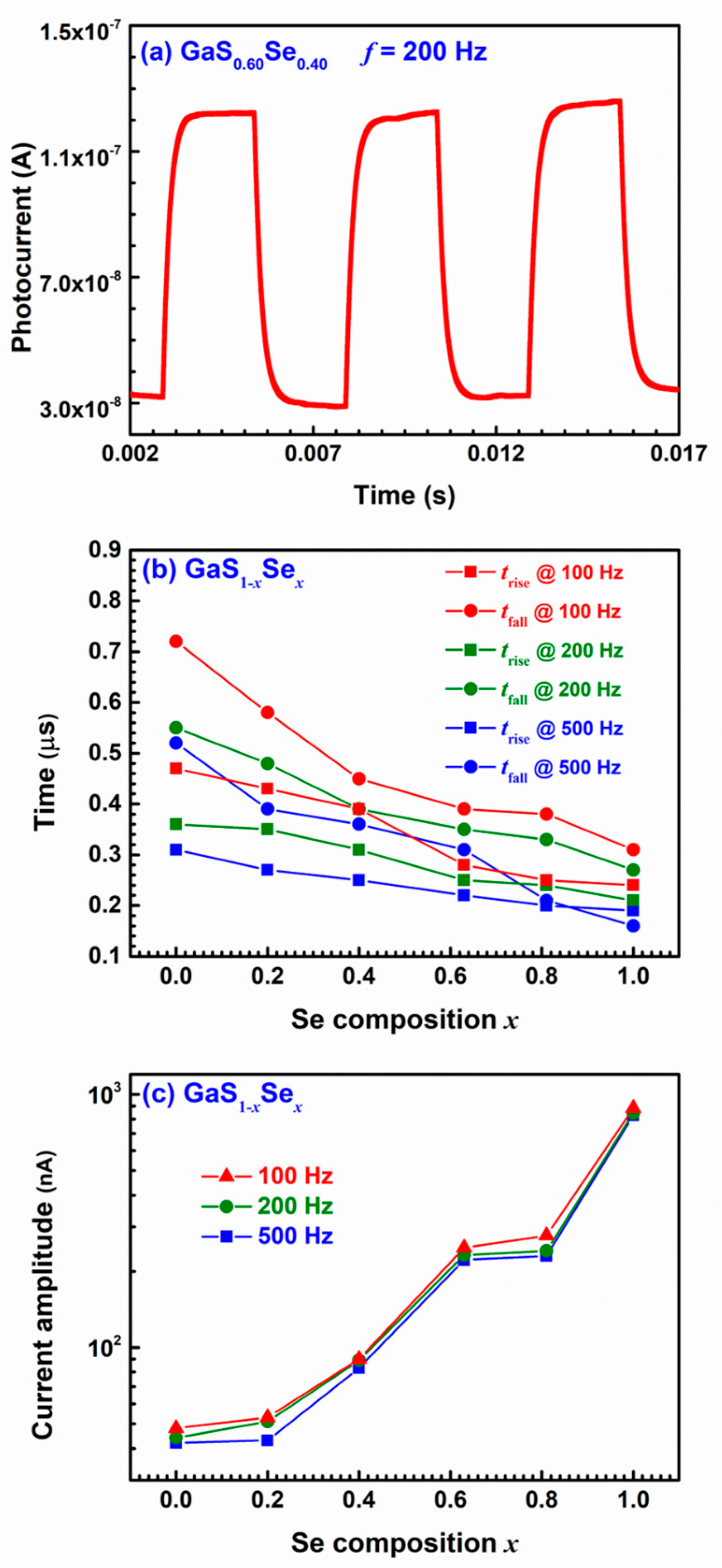
Figure 2a presents the photocurrent profile of the GaS0.60Se0.40 specimen under an illumination frequency of 200 Hz, depicting its variation over time. Similar behaviors were observed for the photocurrents of other GaS1−xSex specimens under different illumination frequencies. Figure 2b illustrates the rise times trise, defined from 10% to 90% of the maximum photocurrent, and the fall times tfall, defined from 90% to 10% of the maximum photocurrent, for the GaS1−xSex samples under various illumination frequencies as functions of the Se composition x. Across all illumination frequencies, trise and tfall decrease with an increase in the Se composition x. The GaSe sample exhibits the shortest trise and tfall.
In Figure 2c, the current amplitudes, representing the difference between the maximum and minimum photocurrents in a rising–falling period, are shown for the GaS1−xSex samples under different illumination frequencies. Regardless of the illumination frequency, the current amplitude rises with an increase in the Se composition x. The pure GaSe sample attains the highest current amplitude, significantly surpassing those of the GaS1−xSex ternary alloy samples and the pure GaS sample. This finding contrasts with previous investigations on both GaS1−xSex nanobelts [37] and MoS2(1−x)Se2x monolayers [45], which indicated a decrease in photocurrent as the Se composition x increased. Our result demonstrates the opposite trend.
Figure 3 illustrates the normalized photocurrents Iac/Idc of the GaS1−xSex specimens as functions of the frequency f of alternating illumination. For frequencies f ≥ 100 Hz, a higher Se composition x corresponds to a greater Iac/Idc. The normalized photocurrents decrease rapidly with increasing f for the pure GaS sample and the GaS1−xSex ternary alloy samples, with the photocurrent dropping more quickly for samples with lower x. For frequencies above 1000 Hz, the Iac/Idc for these samples are less than 0.01. In contrast, the normalized photocurrent for GaSe remains significantly high even at high frequencies, exceeding 0.01 at f = 9000 Hz, with an Iac/Idc greater than 0.015. Consequently, at high frequencies of alternating illumination, the optical response of the pure GaSe sample surpasses that of both the pure GaS sample and the GaS1−xSex ternary alloy samples.
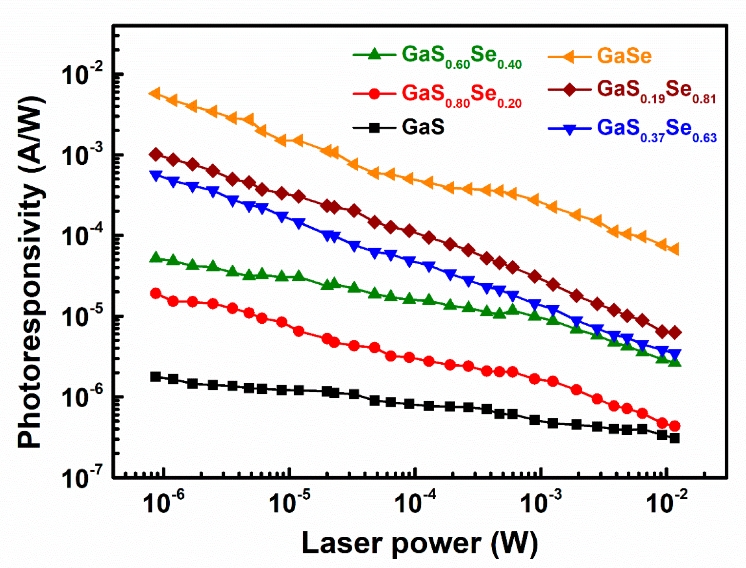
Figure 4 illustrates the photoresponsivities of the GaS1−xSex specimens as functions of the incident laser power. As the incident laser power gradually decreases from the order of 10−2 W to the order of 10−6 W, the photoresponsivities of all GaS1−xSex samples gradually increase. The GaSe sample exhibits the largest increase, with its photoresponsivity increasing by 85.7 times. For a given incident laser power, the photoresponsivity increases as x increases. The pure GaSe sample possesses the highest photoresponsivity at any laser power, exceeding that of other samples by at least one order of magnitude. The maximum photoresponsivity of the pure GaSe sample reaches 5.77 × 10⁻³ A/W at a laser power of 8.70 × 10⁻⁷ W, significantly greater than those of the GaS1−xSex ternary alloy samples and the pure GaS sample. Conversely, the pure GaS sample has the lowest maximum photoresponsivity at a laser power of 8.70 × 10⁻⁷ W, which is 1.78 × 10⁻⁶ A/W.
Figure 5 illustrates how the photoresponsivities of the GaS1−xSex samples vary with the bias voltage. As the applied bias voltage increases from 5 V to 50 V, the photoresponsivities of all GaS1−xSex samples gradually increase. For a given bias voltage, the photoresponsivity increases as x increases. The pure GaSe sample exhibits the highest photoresponsivity at any bias voltage, exceeding that of other samples by at least one order of magnitude. At a bias voltage of 5 V, the photoresponsivities of the GaS1−xSex samples increase from 8.44 × 10⁻⁹ A/W to 3.76 × 10⁻⁶ A/W as x increases from 0 to 1. This contrasts with the findings of Jung et al. [37], who reported that the photoresponsivities of GaS1−xSex nanobelts at 2 V were approximately 7 × 10⁻⁶ A/W for x ranging from 0 to 0.5, decreasing to approximately 1 × 10⁻⁶ A/W for x = 0.7 and approximately 0.5 × 10⁻⁶ A/W for x = 1. Our measured photoresponsivity changes with x in the opposite direction of theirs. The photoresponsivity of our pure GaSe sample reaches its maximum value of 6.39 × 10⁻⁵ A/W at 50 V, significantly greater than those of the GaS1−xSex ternary alloy samples and the pure GaS sample. Conversely, the pure GaS sample has the lowest maximum photoresponsivity at a bias voltage of 50 V, which is 3.34 × 10⁻⁷ A/W.
Ho et al. investigated the photoconductance and photoresponse of the photodetectors based on GaS1−xSex layered crystals, ranking the photosensitivity of their samples from maximum to minimum as GaS0.3Se0.7, GaS0.2Se0.8, GaS0.4Se0.6, GaS0.1Se0.9, GaSe, and GaS [48]. However, our results, as discussed above, differ from those of Ho et al. [48]. We found that the photoresponsive performance of the GaS1−xSex samples improves monotonously with increasing x, with the pure GaSe sample exhibiting the best performance.
The enhancement in photoresponsive performance may be attributed to the decreased bandgaps of the GaS1−xSex samples with increasing x. The redshift of the bandgaps occurs because an increase in the Se composition x results in more S ions being replaced by Se ions, leading to an increase in lattice constants and, consequently, a decrease in bandgaps. A smaller bandgap facilitates the transition of an electron from the valence band to the conduction band by absorbing a photon. The increased number of carriers generated by the absorption of photons enhances the photoresponsive performance of the semiconductors.
Another factor contributing to enhancing the photoresponsive performance of GaS1−xSex layered crystals may be the reduction in the difference between indirect and direct bandgaps as x increases. The minimum difference is only 20 meV when x = 1. This insignificant energy difference makes the GaS1−xSex crystals with high x resemble pseudo-direct bandgap semiconductors [9]. Semiconductors with direct bandgaps exhibit better response to light. Consequently, the photoresponsive performance of the GaS1−xSex crystals is enhanced with increasing x.
It is well known that GaX (X = S or Se) layered crystals exhibit four basic polytypes determined by the stacking sequences of the monolayers: 2H β-, 2H ε-, 3R γ-, and 4H δ-GaX, corresponding to the space groups P63/mmc (D6h4), (D3h1), R3m (C3v5), and P63mc (C6v4) [9]. These distinct stacking arrangements give rise to variations in the properties of GaX crystals across different phases. Building upon this understanding, we propose another intriguing hypothesis suggesting that the photoresponsive performance of GaS1−xSex layered crystals may be influenced by their polytypes. Jung et al. [37] demonstrated that their pure GaS existed in the β phase, while the GaS1−xSex ternary alloys and pure GaSe were in a β-γ mixed phase. With increasing x, the ratio of β to γ phases decreased. Conversely, our pure GaS and GaS0.80Se0.20 ternary alloy were in the β-phase. GaS0.60Se0.40, GaS0.37Se0.63, and GaS0.19Se0.81 ternary alloys exhibited a β-ε mixed phase, with the ratio of β to ε phases decreasing with increasing x. Pure GaSe was in the ε phase. If we hypothesize that the ε and γ phases have the best and worst photoresponsive performance, respectively, with the β phase exhibiting intermediate performance, it may explain the contrast between our findings and those of Jung et al. [37], who reported a decrease in the photoresponsive performance of GaS1−xSex nanobelts with increasing x. However, growing GaS1−xSex crystals exclusively in one pure phase for all different phases remains challenging. Therefore, confirming this hypothesis would require the development of a state-of-the-art growth technique for GaS1−xSex crystals, presenting an intriguing task for future research.
The bandgaps of GaS1−xSex layered crystals span the visible region, but they can significantly increase to over 3.0 eV and extend into the UV region when reduced to the monolayer state due to the quantum confinement effect [36,49]. Photodetectors based on 2D nanoflakes of GaS have shown a remarkable UV-selective photoresponse attributed to the increased bandgaps [23,50,51]. Considering the photoelectric properties of GaS1−xSex layered crystals, the decrease in bandgaps with increasing x implies that GaS1−xSex crystals with x > 0 respond to longer wavelengths compared to pure GaS crystals. Additionally, the enhancement of photoresponsive performance with increasing x suggests that GaS1−xSex crystals with x > 0 exhibit higher photoresponsivity than pure GaS crystals. Consequently, GaS1−xSex-based photodetectors could potentially offer high response and specific wavelength-selectivity for UV and visible-light-detection applications by adjusting their composition and thickness, thereby broadening the potential applications of GaS1−xSex layered crystals in optoelectronics.
4. Conclusions
The photoelectric properties of a complete series of GaS1−xSex (0 ≤ x ≤ 1) layered crystals were investigated. The photoconductivity spectra revealed that the bandgap of GaS1−xSex gradually decreases as the Se composition x increases. The time-dependent photocurrent measurements demonstrated that the increase in x significantly improves the response of GaS1−xSex to light. The pure GaSe crystal has the shortest rise and fall times and the largest current amplitude. The frequency-dependent photocurrent measurements indicated that the photocurrents of the pure GaS crystal and GaS1−xSex ternary alloy crystals decrease rapidly as the frequency of alternating illumination increases. Crystals with lower x have a faster decrease in photocurrent. However, the photocurrent of the pure GaSe crystal persists significantly, even at high frequencies. Additionally, the measurements for laser-power-dependent photoresponsivity and bias-voltage-dependent photoresponsivity revealed that the increase in x enhances the photoresponsivity of GaS1−xSex. Overall, the photoresponsive performance of GaS1−xSex improves with increasing x, with pure GaSe exhibiting the best performance. This result contradicts the findings of the previous report. This enhancement in photoresponsive performance of the GaS1−xSex layered crystals may be attributed to several factors, including decreasing bandgaps, reduced differences between indirect and direct bandgaps, and phase conversion from β-GaS to ε-GaSe as x increases. Because the bandgap and the photoresponsivity of GaS1−xSex vary in reverse trends as x increases, the GaS1−xSex-based photodetectors could potentially offer high response and specific wavelength-selectivity for UV- and visible-light-detection applications by adjusting their composition and thickness. The findings of this work provide novel insights into the photoelectric characteristics of GaS1−xSex layered crystals and contribute to assessing the viability of GaS1−xSex layered crystals for potential use in optoelectronics.
Author Contributions
Conceptualization, Y.-T.S. and D.-Y.L.; methodology, D.-Y.L., M.-C.K. and S.-B.H.; software, D.-Y.L., B.-C.T. and T.-C.H.; validation, Y.-T.S. and D.-Y.L.; formal analysis, Y.-T.S., D.-Y.L. and Y.-M.K.; investigation, Y.-T.S., D.-Y.L. and B.-C.T.; resources, Y.-T.S., D.-Y.L. and Y.-M.K.; data curation, Y.-T.S., B.-C.T. and T.-C.H.; writing—original draft preparation, Y.-T.S.; writing—review and editing, Y.-T.S. and D.-Y.L.; visualization, Y.-T.S. and D.-Y.L.; supervision, Y.-T.S. and D.-Y.L.; project administration, Y.-T.S., D.-Y.L. and Y.-M.K.; funding acquisition, Y.-T.S., D.-Y.L. and Y.-M.K. All authors have read and agreed to the published version of the manuscript.
Funding
This research was funded by the National Science and Technology Council (NSTC) of the Republic of China (Taiwan) under grant numbers NSTC 112-2221-E-018-016 and NSTC 112-2112-M-018-007. The APC was funded by NSTC 112-2221-E-018-016.
Data Availability Statement
Data are contained within the article.
Acknowledgments
The authors would like to express their sincere thanks to H.-K. Teng from the Nan Kai University of Technology for his kind support with equipment and useful comments.
Conflicts of Interest
The authors declare no conflicts of interest.
References
- Terhell, J.C.J.M. Polytypism in the III–VI layer compounds. Prog. Cryst. Growth Charact. 1983, 7, 55–110. [Google Scholar] [CrossRef]
- Cai, H.; Gu, Y.; Lin, Y.-C.; Yu, Y.; Geohegan, D.B.; Xiao, K. Synthesis and emerging properties of 2D layered III–VI metal chalcogenides. Appl. Phys. Rev. 2019, 6, 041312. [Google Scholar] [CrossRef]
- Arora, H.; Erbe, A. Recent progress in contact, mobility, and encapsulation engineering of InSe and GaSe. InfoMat. 2021, 3, 662–693. [Google Scholar] [CrossRef]
- Ho, C.H.; Huang, K.W. Visible luminescence and structural property of GaSe1−xSx (0 ≤ x ≤ 1) series layered crystals. Solid State Comm. 2005, 136, 591–594. [Google Scholar] [CrossRef]
- Ho, C.H.; Lin, S.L. Optical properties of the interband transitions of layered gallium sulfide. J. Appl. Phys. 2006, 100, 083508. [Google Scholar] [CrossRef]
- Kępińska, M.; Nowak, M.; Szalajko, M. Temperature dependence of optical parameters of gallium sulphide. J. Wide Bandgap Mater. 2001, 8, 241–249. [Google Scholar] [CrossRef]
- Isik, M.; Gasanly, N. Composition-tuned band gap energy and refractive index in GaSxSe1−x layered mixed crystals. Mater. Chem. Phys. 2017, 190, 74–78. [Google Scholar] [CrossRef]
- Bube, R.H.; Lind, E.L. Photoconductivity in gallium sulfo-selenide solid solutions. Phys. Rev. 1960, 119, 1535–1537. [Google Scholar] [CrossRef]
- Shih, Y.-T.; Lin, D.-Y.; Tseng, B.-C.; Kao, Y.-M.; Hwang, S.-B.; Lin, C.-F. Structural and optical characterization of GaS1−xSex layered mixed crystals grown by chemical vapor transport. Mater. Today Comm. 2023, 37, 107047. [Google Scholar] [CrossRef]
- Nizametdinpova, Y.A. The refleotion spectrum of GaSe and Gas single crystals near the fundamental absorption edge. Phys. Stat. Sol. 1967, 19, k111–k112. [Google Scholar]
- Fernelius, N.C. Properties of gallium Selenide single crystal. Prog. Cryst. Growth Charact. 1994, 28, 275–353. [Google Scholar] [CrossRef]
- Bube, R.H.; Lind, E.L. Photoconductivity of gallium selenide crystals. Phys. Rev. 1959, 115, 1159–1164. [Google Scholar] [CrossRef]
- Wu, C.C.; Ho, C.H.; Shen, W.T.; Cheng, Z.H.; Huang, Y.S.; Tiong, K.K. Optical properties of GaSe1−xSx series layered semiconductors grown by vertical Bridgman method. Mater. Chem. Phys. 2004, 88, 313–317. [Google Scholar] [CrossRef]
- Madelung, O. Semiconductors: Data Handbook, 3rd ed.; Springer: Marburg, Germany, 2004; p. 515. [Google Scholar]
- Aono, T.; Kase, K.; Kinoshita, A. Near-blue photoluminescence of Zn-doped GaS single crystals. J. Appl. Phys. 1993, 74, 2818–2820. [Google Scholar] [CrossRef]
- Shigetomi, S.; Ikari, T.; Nakashima, H. Impurity levels in layer semiconductor p-GaSe doped with Mn. J. Appl. Phys. 1994, 76, 310–314. [Google Scholar] [CrossRef]
- Chen, M.-W.; Kim, H.; Ovchinnikov, D.; Kuc, A.; Heine, T.; Renault, O.; Kis, A. Large-grain MBE-grown GaSe on GaAs with a Mexican hatlike valence band dispersion. NPJ 2D Mater. 2018, 2, 2. [Google Scholar] [CrossRef]
- Afaneh, T.; Fryer, A.; Xin, Y.; Hyde, R.H.; Kapuruge, N.; Gutiérrez, H.R. Large-area growth and stability of monolayer gallium monochalcogenides for optoelectronic devices. ACS Appl. Nano Mater. 2020, 3, 7879–7887. [Google Scholar] [CrossRef]
- Hu, P.; Wen, Z.; Wang, L.; Tan, P.; Xiao, K. Synthesis of few-layer GaSe nanosheets for high performance photodetectors. ACS Nano 2012, 6, 5988–5994. [Google Scholar] [CrossRef] [PubMed]
- Bassou, A.; Rajira, A.; El-Hattab, M.; Haskouri, J.E.; Murcia-Mascaros, S.; Almaggoussi, A.; Abounadi, A. Structural and optical properties of a layered ε-GaSe thin film under elastic deformation from flexible PET substrate. Micro Nanostruct. 2022, 163, 107152. [Google Scholar] [CrossRef]
- Gutiérrez, Y.; Giangregorio, M.M.; Dicorato, S.; Palumbo, F.; Losurdo, M. Exploring the thickness-dependence of the properties of layered gallium sulfide. Front. Chem. 2021, 9, 781467. [Google Scholar] [CrossRef]
- Curreli, N.; Serri, M.; Zappia, M.I.; Spirito, D.; Bianca, G.; Buha, J.; Najafi, L.; Sofer, Z.; Krahne, R.; Pellegrini, V.; et al. Liquid-phase exfoliated gallium selenide for light-driven thin-film transistors. Adv. Electron. Mater. 2021, 7, 2001080. [Google Scholar] [CrossRef]
- Zappia, M.I.; Bianca, G.; Bellani, S.; Curreli, N.; Sofer, Z.; Serri, M.; Najafi, L.; Piccinni, M.; Oropesa-Nunez, R.; Marvan, P.; et al. Two-dimensional gallium sulfide nanoflakes for UV-selective photoelectrochemical-type photodetectors. J. Phys. Chem. C 2021, 125, 11857–11866. [Google Scholar] [CrossRef] [PubMed]
- Scrocco, M. Electron-energy-loss spectra of GaSe and Ga metal. Phys. Rev. B 1987, 36, 9732–9735. [Google Scholar] [CrossRef] [PubMed]
- Lei, S.; Ge, L.; Liu, Z.; Najmaei, S.; Shi, G.; You, G.; Lou, J.; Vajtai, R.; Ajayan, P.M. Synthesis and photoresponse of large GaSe atomic layers. Nano Lett. 2013, 13, 2777–2781. [Google Scholar] [CrossRef] [PubMed]
- Cao, Y.; Cai, K.; Hu, P.; Zhao, L.; Yan, T.; Luo, W.; Zhang, X.; Wu, X.; Wang, K.; Zheng, H. Strong enhancement of photoresponsivity with shrinking the electrodes spacing in few layer GaSe photodetectors. Sci. Rep. 2015, 5, 8130. [Google Scholar] [CrossRef]
- Karvonen, L.; Säynätjoki, A.; Mehravar, S.; Rodriguez, R.D.; Hartmann, S.; Zahn, D.R.T.; Honkanen, S.; Norwood, R.A.; Peyghambarian, N.; Kieu, K.; et al. Investigation of second- and third- harmonic generation in few-layer gallium selenide by multiphoton microscopy. Sci. Rep. 2015, 5, 10334. [Google Scholar] [CrossRef] [PubMed]
- Zhou, X.; Cheng, J.; Zhou, Y.; Cao, T.; Hong, H.; Liao, Z.; Wu, S.; Peng, H.; Liu, K.; Yu, D. Strong second-harmonic generation in atomic layered GaSe. J. Am. Chem. Soc. 2015, 137, 7994–7997. [Google Scholar] [CrossRef] [PubMed]
- Ahmed, S.; Cheng, P.K.; Qiao, J.; Gao, W.; Saleque, A.M.; Ivan, M.N.A.S.; Wang, T.; Alam, T.I.; Hani, S.U.; Guo, Z.L.; et al. Nonlinear optical activities in two-dimensional gallium sulfide: A comprehensive study. ACS Nano 2022, 16, 12390–12402. [Google Scholar] [CrossRef] [PubMed]
- Arancia, G.; Grandolfo, M.; Manfredotti, C.; Rizzo, A. Electron diffraction study of melt- and vapour-grown GaSe1−xSx single crystals. Phys. Stat. Sol. (a) 1976, 33, 563–571. [Google Scholar] [CrossRef]
- Ho, C.H.; Wu, C.C.; Cheng, Z.H. Crystal structure and electronic structure of GaSe1−xSx series layered solids. J. Crystal Grow. 2005, 279, 321–328. [Google Scholar] [CrossRef]
- Terhell, J.C.J.M.; Lieth, R.M.A. Preparation and crystallography of gallium sulfide-selenide solid solutions. Phys. Stat. Sol. (a) 1971, 5, 719–724. [Google Scholar] [CrossRef]
- Whitehouse, C.R.; Balchin, A.A. Structural studies of compounds in the series GaSxSe1−x (0 ≤ x ≤ 1) grown by iodine vapour transport. J. Mater. Sci. 1978, 13, 2394–2402. [Google Scholar] [CrossRef]
- Aulich, E.; Brebner, J.L.; Mooser, E. Indirect energy gap in GaSe and Gas. Phys. Stat. Sol. 1969, 31, 129–131. [Google Scholar] [CrossRef]
- Mercier, A.; Voitchovsky, J.P. Raman scattering from GaSxSe1−x. Solid State Comm. 1974, 14, 757–762. [Google Scholar] [CrossRef]
- Jung, C.S.; Shojaei, F.; Park, K.; Oh, J.Y.; Im, H.S.; Jang, D.M.; Park, J.; Kang, H.S. Red-to-ultraviolet emission tuning of two-dimensional gallium sulfide/selenide. ACS Nano 2015, 9, 9585–9593. [Google Scholar] [CrossRef] [PubMed]
- Jung, C.S.; Park, K.; Shojaei, F.; Oh, J.Y.; Im, H.S.; Lee, J.A.; Jang, D.M.; Park, J.; Myoung, N.; Lee, C.-L.; et al. Photoluminescence and photocurrents of GaS1−xSex Nanobelts. Chem. Mater. 2016, 28, 5811–5820. [Google Scholar] [CrossRef]
- Asadov, S.M.; Mustafaeva, S.N.; Mammadov, A.N. Thermodynamic assessment of phase diagram and concentration–temperature dependences of properties of solid solutions of the GaS–GaSe system. J. Therm. Anal. Calorim. 2018, 133, 1135–1141. [Google Scholar] [CrossRef]
- Tsuboi, Y.; Urakami, N.; Hashimoto, Y. Photoluminescence of layered semiconductor materials for emission-color conversion of blue micro light-emitting diode (μLED). Coatings 2020, 10, 985. [Google Scholar] [CrossRef]
- Huang, C.-B.; Wu, H.-X.; Ni, Y.-B.; Wang, Z.-Y.; Qi, M.; Zhang, C.-L. First-principles calculation of the structural, electronic, elastic, and optical properties of sulfur-doping ε-GaSe crystal. Chin. Phys. B 2016, 25, 086201. [Google Scholar] [CrossRef]
- Zhang, W.X.; Shi, C.H.; He, C. Novel two-dimensional Ga(In)S1−xSex as high-efficiency OER catalysts for photocatalytic water splitting. J. Solid State Chem. 2020, 292, 121730. [Google Scholar] [CrossRef]
- Wines, D.; Saritas, K.; Ataca, C. A pathway towards high throughput quantum Monte Carlo simulations for alloys: A case study of two-dimensional (2D) GaSxSe1−x. J. Chem. Phys. 2021, 155, 194112. [Google Scholar] [CrossRef] [PubMed]
- Ma, T.; Li, Z.; Zhang, H.; Zhu, C.; Lei, Z.; Yang, C. Electronic, optical and lattice dynamics properties of layered GaSe1−xSx. Mater. Today Comm. 2021, 27, 102212. [Google Scholar] [CrossRef]
- Mosaferi, M.; Sarsari, I.A.; Alaei, M. Band structure engineering in gallium sulfide nanostructures. Appl. Phys. A 2021, 127, 123. [Google Scholar] [CrossRef]
- Klee, V.; Preciado, E.; Barroso, D.; Nguyen, A.E.; Lee, C.; Erickson, K.J.; Triplett, M.; Davis, B.; Lu, I.-H.; Bobek, S.; et al. Superlinear composition-dependent photocurrent in CVD-grown monolayer MoS2(1−x)Se2x alloy devices. Nano Lett. 2015, 15, 2612–2619. [Google Scholar] [CrossRef] [PubMed]
- Tauc, J.; Grigorvici, R.; Vancu, A. Optical properties and electronic structure of amorphous germanium. Phys. Status Solidi 1966, 15, 627–637. [Google Scholar] [CrossRef]
- Tauc, J. Optical properties and electronic structure of amorphous Ge and Si. Mat Res. Mull. 1968, 3, 37–46. [Google Scholar] [CrossRef]
- Ho, C.-H.; Hsieh, M.-H.; Wu, C.-C. Photoconductance and photoresponse of layer compound photodetectors in the UV-visible region. Rev. Sci. Instrum. 2006, 77, 113102. [Google Scholar] [CrossRef]
- Zhuang, H.L.; Hennig, R.G. Single-layer group-III monochalcogenide photocatalysts for water splitting. Chem. Mater. 2013, 25, 3232–3238. [Google Scholar] [CrossRef]
- Lu, Y.; Chen, J.; Chen, T.; Shu, Y.; Chang, R.; Sheng, Y.; Shautsova, V.; Mkhize, N.; Holdway, P.; Bhaskaran, H.; et al. Controlling defects in continuous 2D GaS films for high-performance wavelength-tunable UV-discriminating photodetectors. Adv. Mater. 2020, 32, 1906958. [Google Scholar] [CrossRef]
- Hu, P.; Wang, L.; Yoon, M.; Zhang, J.; Feng, W.; Wang, X.; Wen, Z.; Idrobo, J.C.; Miyamoto, Y.; Geohegan, D.B.; et al. Highly responsive ultrathin GaS nanosheet photodetectors on rigid and flexible substrates. Nano Lett. 2013, 13, 1649–1654. [Google Scholar] [CrossRef]
Figure 1.
Absorption (a) and photoconductivity (b) spectra of the GaS1−xSex specimens at room temperature.
Figure 1.
Absorption (a) and photoconductivity (b) spectra of the GaS1−xSex specimens at room temperature.

Figure 2.
(a) Photocurrent of the GaS0.60Se0.40 specimen under an illumination frequency of 200 Hz as a function of time. Rise times trise and fall times tfall (b) and current amplitudes (c) of the GaS1−xSex specimens under variant frequencies of alternating illumination as functions of the Se composition x.

Figure 3.
Normalized photocurrents of the GaS1−xSex specimens as functions of the frequency of alternating illumination.
Figure 3.
Normalized photocurrents of the GaS1−xSex specimens as functions of the frequency of alternating illumination.

Figure 4.
Photoresponsivities of the GaS1−xSex specimens as functions of the incident laser power.

Figure 5.
Photoresponsivities of the GaS1−xSex specimens as functions of the bias voltage.

Disclaimer/Publisher’s Note: The statements, opinions and data contained in all publications are solely those of the individual author(s) and contributor(s) and not of MDPI and/or the editor(s). MDPI and/or the editor(s) disclaim responsibility for any injury to people or property resulting from any ideas, methods, instructions or products referred to in the content. |
© 2024 by the authors. Licensee MDPI, Basel, Switzerland. This article is an open access article distributed under the terms and conditions of the Creative Commons Attribution (CC BY) license (https://creativecommons.org/licenses/by/4.0/).
Share and Cite
MDPI and ACS Style
Shih, Y.-T.; Lin, D.-Y.; Tseng, B.-C.; Huang, T.-C.; Kao, Y.-M.; Kao, M.-C.; Hwang, S.-B. Photoelectric Properties of GaS1−xSex (0 ≤ x ≤ 1) Layered Crystals. Nanomaterials 2024, 14, 701. https://doi.org/10.3390/nano14080701
AMA Style
Shih Y-T, Lin D-Y, Tseng B-C, Huang T-C, Kao Y-M, Kao M-C, Hwang S-B. Photoelectric Properties of GaS1−xSex (0 ≤ x ≤ 1) Layered Crystals. Nanomaterials. 2024; 14(8):701. https://doi.org/10.3390/nano14080701
Chicago/Turabian StyleShih, Yu-Tai, Der-Yuh Lin, Bo-Chang Tseng, Ting-Chen Huang, Yee-Mou Kao, Ming-Cheng Kao, and Sheng-Beng Hwang. 2024. "Photoelectric Properties of GaS1−xSex (0 ≤ x ≤ 1) Layered Crystals" Nanomaterials 14, no. 8: 701. https://doi.org/10.3390/nano14080701
Note that from the first issue of 2016, this journal uses article numbers instead of page numbers. See further details here.