Three-Dimensional Porous Nitrogen-Doped NiO Nanostructures as Highly Sensitive NO2 Sensors


1
School of Mechanical Engineering, Chonnam National University, 77 Yongbong-ro, Buk-gu, Gwangju 61186, Korea
2
Department of Chemical Engineering, University of South Carolina, 301 Main Street, Columbia, SC 29208, USA
3
School of Chemical Engineering and Bioengineering, University of Ulsan, 93 Daehak-ro, Nam-gu, Ulsan 44610, Korea
4
School of Chemical Engineering, Chonnam National University, 77 Yongbong-ro, Buk-gu, Gwangju 61186, Korea
*
Author to whom correspondence should be addressed.
Nanomaterials 2017, 7(10), 313; https://doi.org/10.3390/nano7100313
Submission received: 11 September 2017
/
Revised: 2 October 2017
/
Accepted: 8 October 2017
/
Published: 11 October 2017
(This article belongs to the Special Issue Nanomaterials for Sensing Applications)
Abstract
:Nickel oxide has been widely used in chemical sensing applications, because it has an excellent p-type semiconducting property with high chemical stability. Here, we present a novel technique of fabricating three-dimensional porous nitrogen-doped nickel oxide nanosheets as a highly sensitive NO2 sensor. The elaborate nanostructure was prepared by a simple and effective hydrothermal synthesis method. Subsequently, nitrogen doping was achieved by thermal treatment with ammonia gas. When the p-type dopant, i.e., nitrogen atoms, was introduced in the three-dimensional nanostructures, the nickel-oxide-nanosheet-based sensor showed considerable NO2 sensing ability with two-fold higher responsivity and sensitivity compared to non-doped nickel-oxide-based sensors.
1. Introduction
Nitrogen dioxide (NO2) is an important air pollutant because it contributes to the formation of photochemical smog, which has significantly harmful impacts on human health. Public awareness about the dangers of NO2 has increased the demand for detecting this hazardous gas with high precision sensors composed of highly sensitive materials. Therefore, numerous approaches have been suggested to detect NO2 at the ppm level [1,2,3]. Among the various types of gas sensors, semiconducting metal oxide gas sensors have attracted much attention because of their low cost, ease of production, simplicity of use, and ability to detect numerous gases, e.g., those using tungsten trioxide, titanium dioxide, vanadium oxide, tin dioxide, and nickel oxide (NiO) [4,5,6].
NiO, a well-known stable p-type semiconducting metal oxide, has a high melting point (1960 °C) and excellent chemical stability. Therefore, it has been extensively employed as electrodes in lithium ion batteries and supercapacitors, as electro-catalysts in combustion gas sensing, and in electrochromic devices [7,8,9]. Furthermore, a novel nanostructure with a high specific surface area is essential for enhanced performance of the NiO-based devices, which can be achieved by reactive sputtering, sol–gel methods, and hydrothermal treatments [10,11,12,13,14]. Therefore, highly porous NiO nanostructures can be used to fabricate highly sensitive gas sensors, especially for NO2 detection, because the p-type semiconducting NiO can effectively donate electrons to the NO2 molecules.
Previous studies have reported that nitrogen (N) is a good dopant in many metal oxides because N and oxygen have similar ionic radii [15,16,17]. N-doping in titanium dioxide effectively improved its electro-catalytic performance in the carbon monoxide gas reaction [18], and promoted NO2 adsorption as proven theoretically via density functional theory calculation [19]. Furthermore, the intrinsic electrical resistance and signal noise level of metal oxides could be overcome via N-doping [20,21,22].
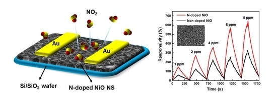
Herein, we present three-dimensional porous N-doped NiO nanosheets (NSs) for highly sensitive NO2 sensing applications. The elaborate NiO nanostructure was prepared by a simple and effective solution-based hydrothermal method [23,24]. Subsequently, N-doping was achieved by thermal treatment with ammonia gas. Figure 1 shows the N-doped NiO nanostructure used in NO2 sensing. The N-doped NiO nanostructure is hydrothermally grown on a silicon/silicon dioxide (Si/SiO2) wafer and gold (Au) electrodes are deposited to measure the electrical signals during NO2 exposure. Owing to the N-doping effect with hierarchical nanostructure, the resistance change in the gas sensor can be greatly amplified. The result shows that the N-doped NiO-based gas sensor, compared to a non-doped sensor, exhibits a two-fold higher responsivity and sensitivity toward NO2 gas detection and is thus a candidate for highly sensitive NO2 sensors.
2. Materials and Methods
2.1. Synthesis of the NiO Nanostructure
The three-dimensional porous NiO nanostructure was synthesized via sequential seeding and growth [23,24], and all reagents were purchased from Sigma-Aldrich, Korea. Nickel acetate tetrahydrate (0.2 M) was dissolved in a mixture of 2-methoxyethanol (6 mL) and diethanolamine (0.25 mL) to obtain an NiO seed solution. After the seed solution was stirred for 2 h at room temperature, it was spin-coated at 4000 rpm for 30 s on an Si/SiO2 wafer and dried on a hot-plate at 250 °C for 15 s. After the spin-coating process was repeated three times, the sample was annealed at 400 °C for 2 h in a vacuum chamber. Note that a higher rotating speed and a longer spinning time may produce an irregular and/or thin coating layer owing to excessive centrifugal force. Here, we found that the above condition was optimal for constructing uniform and stable seed layer with strong adhesion on the substrate [23]. At the next stage, an NiO growth solution was prepared by dissolving nickel nitrate hexahydrate (5.8 g) and hexamethylenetetramine (4.8 g) in distilled (DI) water (100 mL). The NiO-seed-coated wafer was dipped in the growth solution at 90 °C for 2 h, rinsed with DI water, and annealed at 350 °C for 1 h. The annealing process was performed in a gas chamber filled with argon (1 atm) and ammonia (50 sccm) for N-doping. Au electrodes were then deposited on the surface of the N-doped NiO nanostructure via thermal evaporation in vacuum.
2.2. Chracterization of the N-Doped NiO Nanostructure
The porous morphology of the synthesized NiO nanostructure was investigated by scanning electron microscopy (SEM, JEOL JSM-6500FE, Tokyo, Japan). X-ray diffraction (XRD) measurements were carried out to identify the crystal structure of NiO using a high-resolution X-ray diffractometer (Rigaku, D/MAXZ-2500V, Tokyo, Japan). The Brunauer–Emmett–Teller (BET) specific surface areas of the powders were determined by nitrogen adsorption in a Micromeritics ASAP 2020 (Norcross, GA, USA) nitrogen adsorption apparatus. Successful N-doping was examined by X-ray photoelectron spectroscopy (XPS) using a Thermo Fisher Scientific ESCALAB 250Xi (Waltham, MA, USA). The gas sensing properties were evaluated by measuring the resistance change with a Hewlett-Packard 4155A semiconductor parametric analyzer in a MST-5000 gas chamber (MS-Tech, Hwasung, Gyeonggi-do, Korea). In order to measure the electrical resistance, an Au layer consisting of electrodes was deposited on the surface of the N-doped NiO nanostructure using a thermal evaporator with a patterned mask. The thickness of the Au coat was 50 nm from the top surface of the NiO nanostructure and had a 10 μm spacing. The concentration of NO2 was carefully controlled using a mass flow controller (GMC 1200, ATOVAC, Yongin, Gyeonggi-do, Korea).
3. Results and Discussion
3.1. Morphology of the N-Doped NiO-NS Nanostructure
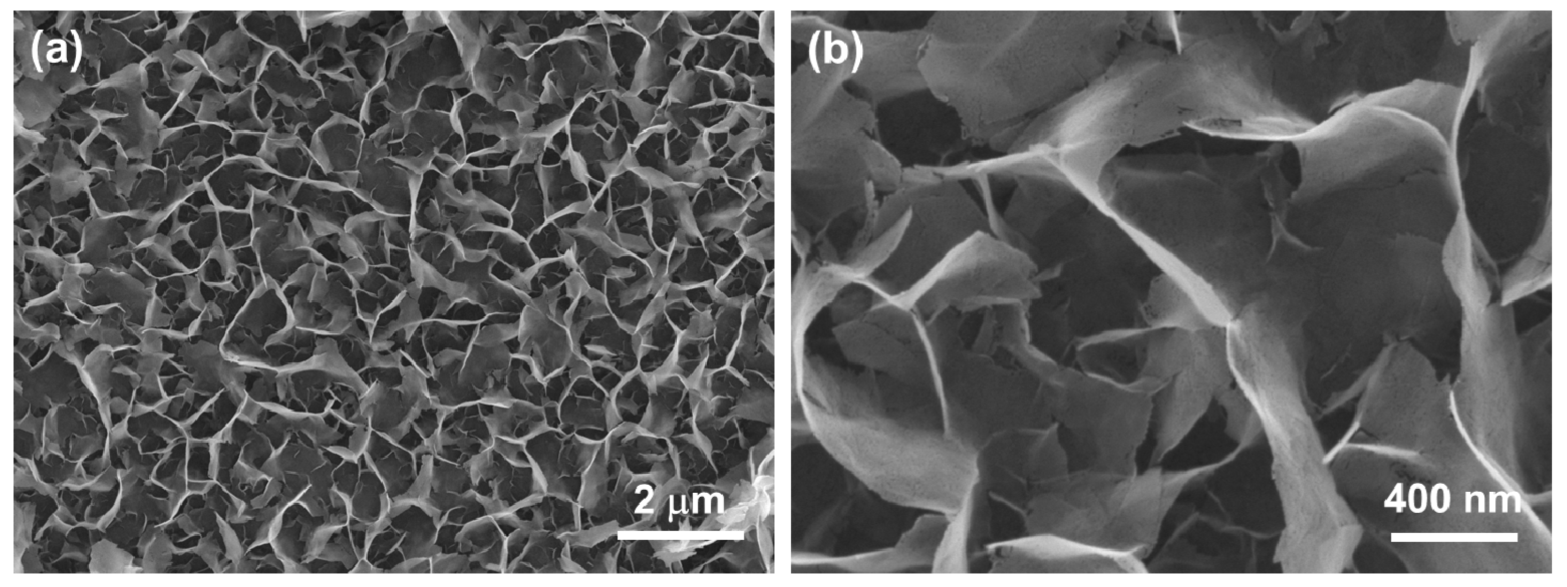
The three-dimensional porous nanostructure of N-doped NiO NSs (Figure 2) shows that the thickness and height of the grown NSs were 20–30 nm and 1–3 μm, respectively, in close agreement with the previously reported values [23,24]. The porous nanostructure hierarchically grown on the wafer had a high surface area of ~205 m2/g, suggesting an enhanced gas adsorption ability, and can thus be applied in high-performance NO2 sensors. Energy-dispersive X-ray spectrometry (EDS) mapping analysis of the elements is shown in Figure 3. Uniformly dispersed green and red dots on the N-doped NiO NSs indicate the successful growth of NiO nanosheets. Note that the N-mapping in the EDS spectrum was somewhat unclear owing to the strong intensity of Ni and O. The identification of the N element was examined via XPS analysis.
3.2. Crystallinity of the N-Doped NiO NS
Figure 4 shows three distinguishable diffraction peaks at 37.2°, 43.5°, and 62.3°, corresponding to the (111), (200), and (220) NiO planes, respectively, indicating high crystallinity for both N-doped and non-doped NiO NSs [7,20,24]. All reflections in the XRD pattern can be indexed to face-centered-cubic-phase NiO (JCPDS card #47-1049) [25]. Since both peak positions and intensities are almost the same for N-doped and non-doped NiO NSs, it can be concluded that doping by nitrogen atoms has no influence on the intrinsic crystal structure of NiO. The high peak intensity indicates that the prepared NiO NSs are highly crystalline. Moreover, for the N-doped NiO NSs, crystallinity higher than that of the non-doped NiO NSs can also be verified by calculating the grain sizes from crystallographic parameters. The Scherrer’s formula was used to calculate the crystallite size D of the manufactured NiO NSs using Equation (1) [26,27]:
where λ is the wavelength of the X-ray source (1.54 Å), β is the full width at half maximum of high-intensity peaks, and θ is the Bragg’s angle [28,29]. The obtained β and D values are listed in Table 1, where the N-doped NiO NSs have relatively larger grain sizes than those of the non-doped NSs. Therefore, it can be estimated that N-doping can increase the crystallinity of NiO NSs. The Scherrer equation is generally applicable for spherical particles; it has limitations because many factors may contribute to peak broadening in the XRD patterns. For example, the deposition and growth of materials on substrates may produce crystallographic strain due to residual stress. Herein, assuming the same circumstance for N-doped and non-doped NiO NSs, we investigated only their relative crystallinities.
3.3. Chemical Characterization of the N-Doped NiO NSs
The chemical structure of NiO was examined, and N-doping was confirmed using XPS analyses. Both N-doped and non-doped NiO NSs showed the peaks of O 1s and Ni 2p (Figure 5), with two split peaks of 2p1/2 (872.1 eV) and 2p3/2 (853.2 eV), and a satellite peak of 2p3/2 (860.1 eV) [30,31]. A peak of N 1s was only observed in N-doped NiO, which indicates the existence of nitrogen atoms in N-doped NiO (Figure 5a). The high-resolution N 1s peak of N-doped NiO was deconvoluted into two peaks corresponding to pyridinic and pyrrolic nitrogen components (398.5 and 400.1 eV, respectively) [32,33]. The presence of these nitrogen species confirms N-doping on the surface of NiO NSs.
3.4. NO2 Sensing Performance of the N-Doped NiO NSs Nanostructure
In order to elucidate the NO2 sensing performance of the synthesized NiO nanostructures, gas sensing tests were performed at 200 °C by exposing to various concentrations of NO2, from 1 to 8 ppm. Here, the exposing time was 125 s. NO2 was injected into the measurement chamber (200 °C) with N2. For a quantitative examination, the responsivity (RS) and sensitivity (k) were investigated with respect to the gas concentration, as defined in Equations (2) and (3):
where Ratm is the resistance of the sensors measured under air circumstance and RG is the resistance when NO2 gas is injected with the carrier gas. The value of k was obtained from the slope of the best linear fitting line in the plots of maximum responsivity (RSmax) versus NO2 concentration (CG). Note that Ratm was measured as 13.5 kΩ. Figure 6a shows that RS increased when the sensor was exposed to NO2 because RG decreases due to the p-type semiconducting characteristic of NiO, where the Ni2+ vacancies contribute to the hole-conduction [34]. After NO2 disposal, RS was reinstated to its initial stage condition, which represents reversible adsorption and desorption of NO2 on the surface of NiO. The N-doped NiO-NS-based sensor exhibited a two-fold higher RS than that of the non-doped device, which can also be confirmed by its two-fold higher k value in Figure 6b. Thus, there is a linear relationship between responsivity and NO2 concentration in both types of sensors. Hence, the NiO-NS-based device can be used as quantitative high-precision gas sensors to measure NO2 concentrations.
Note that other reducing gases such as H2S, NH3, and H2 are also applicable to N-doped NiO NS gas sensors. Because the sensing behaviors of these gases show negative responsivities with increasing values of RG [24], selective sensing with the reducing gases and NO2 is possible when the NiO-NS-based gas sensors. However, the absolute values of responsivities for such reducing gases were still low (less than 50%). Therefore, it is further required to develop an innovative n-type semiconducting material, which is highly sensitive toward the reducing gases.
Even though NO can be considered for use with this gas sensor, direct use is limited because NO reacts well with O2 and produces NO2 easily under a working temperature of 200 °C. In this case, we kept the working temperature at 200 °C when degassing NO2 after sensing in order to remove residual and adsorbed NO2. Even though the measurement was performed by co-injecting N2 gas, the circumstances under vacuum were not ideal. Therefore, NO can be reacted with residual O2 at this high working temperature, and the precise amount of NO2 then becomes hard to control.
3.5. N-Doping Effect on the NiO NSs
The enhanced NO2 sensing performance of the N-doped NiO device is because of the increase in p-type conductivity (p+-type) and the decrease in material resistance by nitrogen doping. Generally, in non-doped NiO, electrical conduction occurs via the hole hopping of Ni2+ vacancies, where each vacancy contributes two holes for conduction associated with a p-type semiconducting characteristic. Moreover, oxygen vacancies act as shallow donors, which are responsible for n-type conductivity. Therefore, the NO2 molecules adsorbed to the NiO NS surfaces (NO2 (ads)) accept electrons from the NiO surface, and this results in the generation of holes (h+) as per Equation (4):
When NO2 is adsorbed on the N-doped NiO surface, holes are generated on the surface by an electron transfer mechanism to the NO2 molecules. Then, the holes on the N-doped NiO surfaces are transferred to the non-doped NiO surface (p-type). This hole-transfer at the p+–p heterojunction leads to a decrease in resistance of the NiO backbone, which carries charges between the two electrodes [35,36]. Without such heterojunctions, the generated holes are likely to accumulate on the NiO surface, causing relatively low responsivity owing to the suppression of further adsorption of NO2 molecules. Therefore, the p+–p heterojunctions can relieve the amassed holes and can promote the continuous adsorption of NO2, which results in the high responsivity and sensitivity of the sensors. Therefore, the synergetic effect of the p-type semiconducting property of NiO and the p-type doping of N increased the performance of the NO2 sensing.
3.6. Repetitive and Saturate Responses of the N-Doped NiO-NSs-Based NO2 Sensor
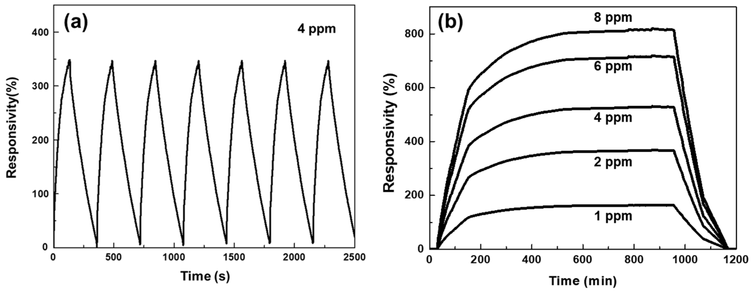
Furthermore, in order to examine the stability of the N-doped NiO-nased gas sensor, a repetitive NO2 gas sensing test was performed at a specific NO2 gas concentration of 4 ppm. The NO2 gas flow was controlled by sequentially turning on (125 s) and turning off (250 s) and the test was done at 200 °C. As shown in Figure 7a, the synthesized gas sensor exhibited stable reversibility of the gas sensing characteristics under repetitive NO2 exposure conditions, supporting its potential application in NO2 sensors, where cycle-to-cycle variation can be successfully removed. For every cycle, the N-doped NiO-based sensor showed highly amplified responsivity (resistance change) upon NO2 exposure and fully recovered signals in the absence of NO2 with good repetitive switching behaviors. With high sensitivity, highly stable, and repetitive gas sensing performance was observed, which suggests that the presented N-doped NiO nanostructure-based device has great potential for applications in quantitatively reliable sensors to precisely measure NO2 gas.
Additionally, the N-doped NiO-based sensor showed stable saturate responses for all different concentrations of NO2, as shown in Figure 7b. After certain injection times, the values of responsivities exhibited steady-state behaviors, which confirms that the developed sensor can give reproducible responses for detecting NO2. For the saturate response, the value of ksat (Equation (3)) was calculated as 90.13 ppm−1 by linear-fitting (root mean square = 0.96). This result shows that N-doped NiO-NS-based gas sensors are highly sensitive toward NO2 gas. Note that previous work using the non-doped NiO NS on a graphene substrate showed k = 32.4 ppm−1. Because the measurement circumstance was kept at a working temperature of 200 °C, even after the gas sensing by NO2 injection, all residual and adsorbed gases could be fully removed from the NiO NSs. Therefore, the device can exhibit stable responses for long-term cycle. It is noted that the N-doped NiO-based gas sensor showed negligible change on repetitive and saturate responses after one month.
4. Conclusions
NiO has been widely used in chemical sensing applications, because it has an excellent p-type semiconducting property and high chemical stability. Here, in order to develop highly sensitive and stable NO2 sensors, we successfully fabricated three-dimensional porous N-doped NiO NSs by a simple and effective hydrothermal technique. N-doping of this novel NiO NS led to significantly enhanced NO2 sensing performance with a two-fold higher responsivity and sensitivity compared to non-doped NiO NS nanostructure. This was achieved by constructing p+–p heterojunctions at the N-doped NiO sites. The novel N-doped NiO nanostructure-based device exhibited high sensitivity and stability with good repetitive gas sensing performance. Hence, it is a candidate of choice for quantitatively reliable high-precision gas sensors for the measurement of NO2 gas.
Acknowledgments
This work was supported by the National Research Foundation (NRF) of Korea, a grant funded by the Ministry of Science, ICT and Future Planning (2015R1A2A2A04003160 and 2016M3A7B4021149).
Author Contributions
Wonoh Lee and Seung Hyun Hur designed the research project. Van Hoang Luan, Huynh Ngoc Tien, and Seung Hyun Hur conceived and designed the experiments; Van Hoang Luan and Huynh Ngoc Tien performed the experiments and analyzed the data; Van Hoang Luan, Jong Hun Han, and Wonoh Lee wrote the paper; all authors discussed and commented on the manuscript.
Conflicts of Interest
The authors declare no conflict of interest.
References
- Hjiri, M.; El Mir, L.; Leonardi, S.G.; Donato, N.; Neri, G. CO and NO2 selective monitoring by ZnO-based sensors. Nanomaterials 2013, 3, 357–369. [Google Scholar] [CrossRef] [PubMed]
- Duvall, R.M.; Long, R.W.; Beaver, M.R.; Kronmiller, K.G.; Wheeler, M.L.; Szykman, J.J. Performance evaluation and community application of low-cost sensors for ozone and nitrogen dioxide. Sensors 2016, 16, 1698. [Google Scholar] [CrossRef] [PubMed]
- Zhang, S.; Hang, N.T.; Zhang, Z.; Yue, H.; Yang, W. Preparation of g-C3N4/graphene composite for detecting NO2 at room temperature. Nanomaterials 2017, 7, 12. [Google Scholar] [CrossRef] [PubMed]
- Capone, S.; Rella, R.; Siciliano, P.; Vasanelli, L. A comparison between V2O5 and WO3 thin films as sensitive elements for NO detection. Thin Solid Films 1999, 350, 264–268. [Google Scholar] [CrossRef]
- Diéguez, A.; Romano-Rodríguez, A.; Alay, J.L.; Morante, J.R.; Bârsan, N. Parameter optimisation in SnO2 gas sensors for NO2 detection with low cross-sensitivity to CO: Sol–gel preparation, film preparation, powder calcination, doping and grinding. Sens. Actuators B Chem. 2000, 65, 166–168. [Google Scholar]
- Cheng, J.P.; Wang, J.; Li, Q.Q.; Liu, H.G.; Li, Y. A review of recent developments in tin dioxide composites for gas sensing application. J. Ind. Eng. Chem. 2016, 44, 1–22. [Google Scholar] [CrossRef]
- Luan, V.H.; Chung, J.S.; Hur, S.H. Preparation of a reduced graphene oxide hydrogel by Ni ions and its use in a supercapacitor electrode. RSC Adv. 2015, 5, 22753–22758. [Google Scholar] [CrossRef]
- Xia, X.H.; Tu, J.P.; Zhang, J.; Wang, X.L.; Zhang, W.K.; Huang, H. Electrochromic properties of porous NiO thin films prepared by a chemical bath deposition. Sol. Energy Mater. Sol. Cells 2008, 92, 628–633. [Google Scholar] [CrossRef]
- Varghese, B.; Reddy, M.V.; Yanwu, Z.; Lit, C.S.; Hoong, T.C.; Subba Rao, G.V.; Chowdari, B.V.R.; Wee, A.T.S.; Lim, C.T.; Sow, C.H. Fabrication of NiO nanowall electrodes for high performance lithium ion battery. Chem. Mater. 2008, 20, 3360–3367. [Google Scholar] [CrossRef]
- Garcia-Miquel, J.L.; Zhang, Q.; Allen, S.J.; Rougier, A.; Blyr, A.; Davies, H.O.; Jones, A.C. Nickel oxide sol-gel films from nickel diacetate for electrochromic applications. Thin Solid Films 2003, 424, 165–170. [Google Scholar] [CrossRef]
- Kuang, D.B.; Lei, B.X.; Pan, Y.P.; Yu, X.Y.; Su, C.Y. Fabrication of novel hierarchical β-Ni(OH)2 and NiO microspheres via an easy hydrothermal process. J. Phys. Chem. C 2009, 113, 5508–5513. [Google Scholar] [CrossRef]
- Vučinić-Vasić, M.; Antic, B.; Kremenović, A.; Nikolic, A.S.; Stoiljkovic, M.; Bibic, N.; Spasojevic, V.; Colomban, P. Zn, Ni ferrite/NiO nanocomposite powder obtained from acetylacetonato complexes. Nanotechnology 2006, 17, 4877–4884. [Google Scholar]
- Kwak, B.S.; Choi, B.H.; Ji, M.J.; Park, S.M.; Kang, M. Synthesis of spherical NiO nanoparticles using a solvothermal treatment with acetone solvent. J. Ind. Eng. Chem. 2012, 18, 11–15. [Google Scholar] [CrossRef]
- Meng, T.; Xu, Q.Q.; Li, Y.T.; Chang, J.L.; Ren, T.Z.; Yuan, Z.Y. Nickle nanoparticles highly dispersed on reduced graphene oxide for ammonia decomposition to hydrogen. J. Ind. Eng. Chem. 2015, 32, 373–379. [Google Scholar] [CrossRef]
- Minegishi, K.; Koiwai, Y.; Kikuchi, Y.; Yano, K.; Kasuga, M.; Shimizu, A. Growth of p-type zinc oxide films by chemical vapor deposition. Jpn. J. Appl. Phys. 1997, 36, L1453–L1455. [Google Scholar] [CrossRef]
- Joseph, M.; Tabata, H.; Kawai, T. p-Type electrical conduction in ZnO thin films by Ga and N codoping. Jpn. J. Appl. Phys. 1999, 38, L1205–L1207. [Google Scholar] [CrossRef]
- Look, D.C.; Reynolds, D.; Litton, C.; Jones, R.; Eason, D.; Cantwell, G. Characterization of homoepitaxial p-type ZnO grown by molecular beam epitaxy. Appl. Phys. Lett. 2002, 81, 1830–1832. [Google Scholar] [CrossRef]
- Liu, G.; Li, F.; Wang, D.W.; Tang, D.M.; Liu, C.; Ma, X.; Lu, G.Q.; Cheng, H.M. Electron field emission of a nitrogen-doped TiO2 nanotube array. Nanotechnology 2008, 19, 025606–025611. [Google Scholar] [CrossRef] [PubMed]
- Liu, J.; Dong, L.; Guo, W.; Liang, T.; Lai, W. First principles study of nitrogen doping at the anatase TiO2 (101) surface. J. Phys. Chem. C 2013, 117, 13037–13044. [Google Scholar] [CrossRef]
- Abbasi, A.; Sardroodi, J.J. N-doped TiO2 anatase nanoparticles as a highly sensitive gas sensor for NO2 detection: Insights from DFT computations. Environ. Sci. Nano 2016, 3, 1153–1164. [Google Scholar] [CrossRef]
- Livraghi, S.; Paganini, M.C.; Giamello, E.; Selloni, A.; Di Valentin, C.; Pacchioni, G. Origin of photoactivity of nitrogen-doped titanium dioxide under visible light. J. Am. Chem. Soc. 2006, 128, 15666–15671. [Google Scholar] [CrossRef] [PubMed]
- Asahi, R.; Morikawa, T.; Ohwaki, T.; Aoki, K.; Taga, Y. Visible-light photocatalysis in nitrogen-doped titanium oxides. Science 2001, 293, 269–271. [Google Scholar] [CrossRef] [PubMed]
- Xia, Q.X.; Hui, K.S.; Hui, K.N.; Hwang, D.H.; Lee, S.K.; Zhou, W.; Cho, Y.R.; Kwon, S.H.; Wang, Q.M.; Son, Y.G. A facile synthesis method of hierarchically porous NiO nanosheets. Mater. Lett. 2012, 69, 69–71. [Google Scholar] [CrossRef]
- Hoa, L.T.; Tien, H.N.; Luan, V.H.; Chung, J.S.; Hur, S.H. Fabrication of a novel 2D-graphene/2D-NiO nanosheet-based hybrid nanostructure and its use in highly sensitive NO2 sensors. Sens. Actuators B Chem. 2013, 185, 701–705. [Google Scholar] [CrossRef]
- Zhang, G.; Yu, L.; Hoster, H.E.; Lou, X.W. Synthesis of one-dimensional hierarchical NiO hollow nanostructures with enhanced supercapacitive performance. Nanoscale 2013, 5, 877–881. [Google Scholar] [CrossRef] [PubMed]
- Irwin, M.D.; Servaites, J.D.; Buchholz, D.B.; Leever, B.J.; Liu, J.; Emery, J.D.; Zhang, M.; Song, J.J.; Durstock, M.F.; Freeman, A.J.; et al. Structural and electrical functionality of NiO interfacial films in bulk heterojunction organic solar cells. Chem. Mater. 2011, 23, 2218–2226. [Google Scholar] [CrossRef]
- Atay, F.; Bilgin, V.; Akyuz, I.; Kose, S. The effect of in doping on some physical properties of CdS films. Mater. Sci. Semicond. Process. 2003, 6, 197–203. [Google Scholar] [CrossRef]
- Haranath, D.; Sahai, S.; Joshi, A.G.; Gupta, B.K.; Shanker, V. Investigation of confinement effects in ZnO quantum dots. Nanotechnology 2009, 20, 425701–425707. [Google Scholar] [CrossRef] [PubMed]
- Zhu, W.; Lu, C.H.; Chang, F.C.; Kuo, S.W. Supramolecular ionic strength-modulating microstructures and properties of nacre-like biomimetic nanocomposites containing high loading clay. RSC Adv. 2012, 2, 6295–6305. [Google Scholar] [CrossRef]
- Chen, H.L.; Lu, Y.M.; Hwang, W.S. Effect of film thickness on structural and electrical properties of sputter-deposited nickel oxide films. Mater. Trans. 2005, 46, 872–879. [Google Scholar] [CrossRef]
- Biju, V.; Khadar, M.A. Electronic structure of nanostructured nickel oxide using Ni 2p XPS analysis. J. Nanopart. Res. 2002, 4, 247–253. [Google Scholar] [CrossRef]
- Biesinger, M.C.; Payne, B.P.; Lau, L.W.M.; Gerson, A.; St Smart, R.C. X-ray photoelectron spectroscopic chemical state quantification of mixed nickel metal, oxide and hydroxide systems. Surf. Interface Anal. 2009, 41, 324–332. [Google Scholar] [CrossRef]
- Zhuang, Z.; Giles, S.A.; Zheng, J.; Jenness, G.R.; Caratzoulas, S.; Vlachos, D.G.; Yan, Y. Nickel supported on nitrogen-doped carbon nanotubes as hydrogen oxidation reaction catalyst in alkaline electrolyte. Nat. Commun. 2016, 7, 10141. [Google Scholar] [CrossRef] [PubMed]
- Delegan, N.; Daghrir, R.; Drogui, P.; El Khakani, M.A. Bandgap tailoring of in-situ nitrogen-doped TiO2 sputtered films intended for electrophotocatalytic applications under solar light. J. Appl. Phys. 2014, 116, 153510–153518. [Google Scholar] [CrossRef]
- Biju, V.; Khadar, M. Dielectric properties of nanostructured nickel oxide. J. Mater. Sci. 2003, 38, 4055–4063. [Google Scholar] [CrossRef]
- Vasu, K.; Sreedhara, M.B.; Ghatak, J.; Rao, C.N.R. Atomic layer deposition of p-type epitaxial thin films of undoped and N-doped anatase TiO2. ACS Appl. Mater. Interfaces 2016, 8, 7897–7901. [Google Scholar] [CrossRef] [PubMed]
Figure 1.
A schematic illustration and a top-view image of a three-dimensional porous N-doped NO2 gas sensor based on NiO nanosheets (NSs).
Figure 1.
A schematic illustration and a top-view image of a three-dimensional porous N-doped NO2 gas sensor based on NiO nanosheets (NSs).
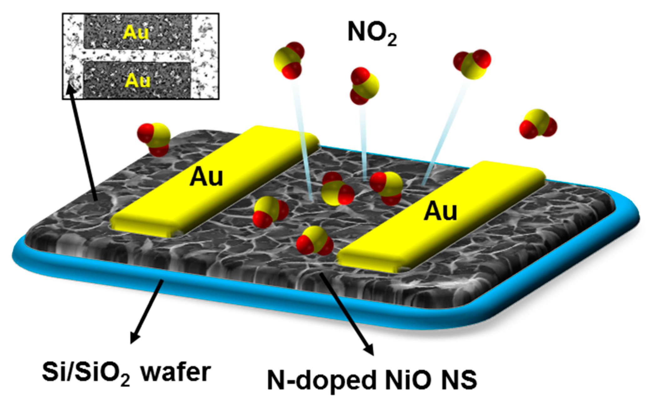
Figure 2.
SEM images of (a) the three-dimensional nanostructure of N-doped NiO NSs and (b) its magnified image.
Figure 2.
SEM images of (a) the three-dimensional nanostructure of N-doped NiO NSs and (b) its magnified image.

Figure 3.
EDS mapping images of N-doped NiO NSs (scale bar = 4 μm).
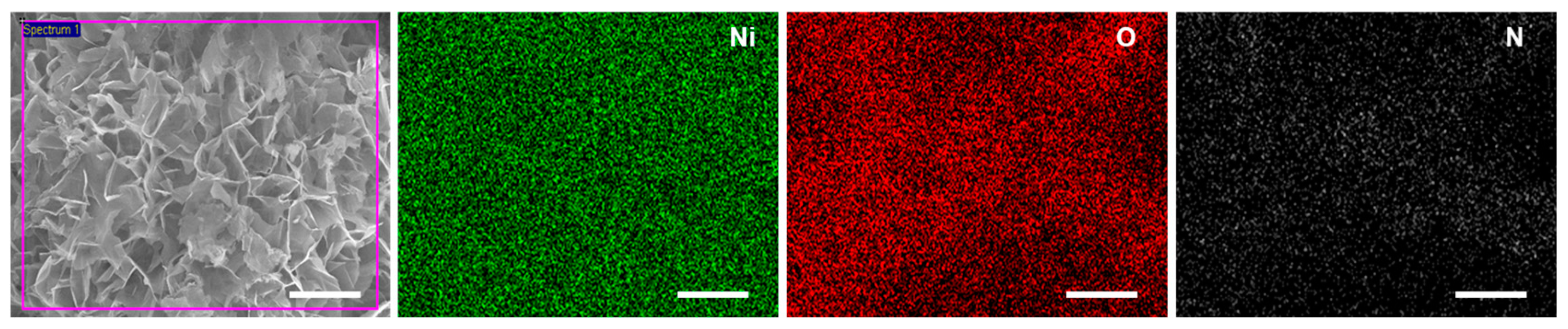
Figure 4.
XRD results of N-doped and non-doped NiO NSs.
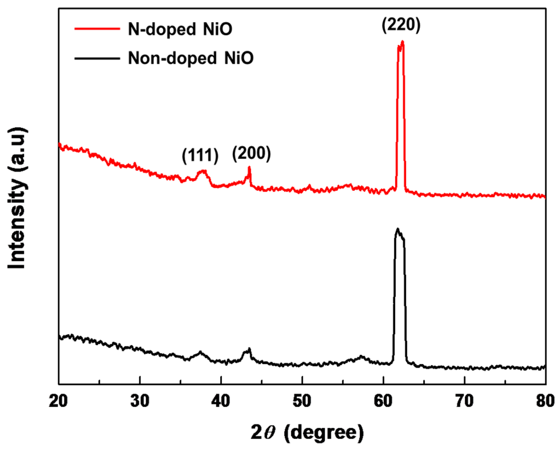
Figure 5.
XPS spectra of N-doped and non-doped NiO NSs: (a) wide scan spectra and (b) N 1s spectra of N-doped NiO with deconvoluted peaks.
Figure 5.
XPS spectra of N-doped and non-doped NiO NSs: (a) wide scan spectra and (b) N 1s spectra of N-doped NiO with deconvoluted peaks.
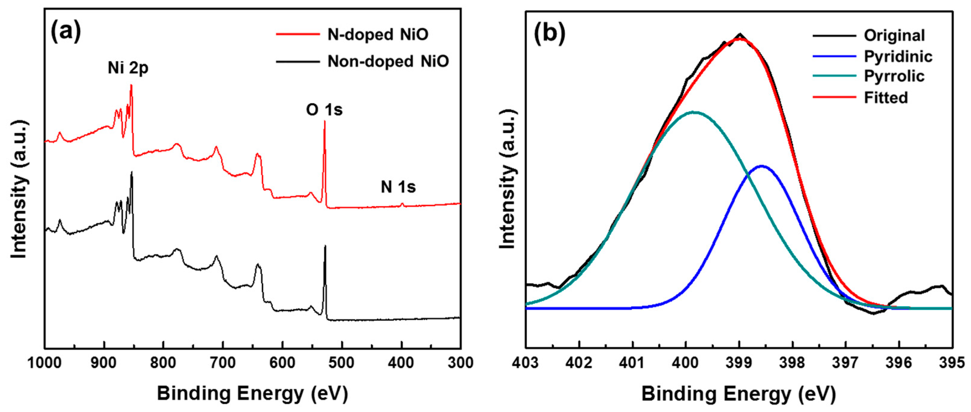
Figure 6.
NO2 sensing performance of N-doped and non-doped NiO NSs: (a) responsivity to various gas concentrations and (b) sensitivity plots.
Figure 6.
NO2 sensing performance of N-doped and non-doped NiO NSs: (a) responsivity to various gas concentrations and (b) sensitivity plots.
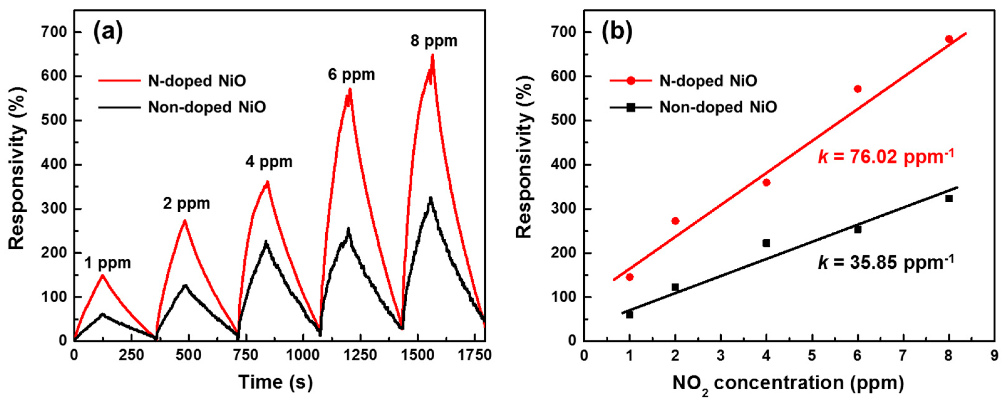
Figure 7.
(a) Repetitive and (b) saturate responses of the N-doped NiO-NS-based NO2 sensors.

Table 1.
Structural crystal parameters of N-doped and non-doped NiO NSs.
| Sample | β (Deg) | D (nm) |
|---|---|---|
| N-doped NiO | 0.65 ± 0.02 | 26.3 ± 0.8 |
| Non-doped NiO | 1.42 ± 0.05 | 12.0 ± 0.5 |
© 2017 by the authors. Licensee MDPI, Basel, Switzerland. This article is an open access article distributed under the terms and conditions of the Creative Commons Attribution (CC BY) license (http://creativecommons.org/licenses/by/4.0/).
Share and Cite
MDPI and ACS Style
Luan, V.H.; Tien, H.N.; Hur, S.H.; Han, J.H.; Lee, W. Three-Dimensional Porous Nitrogen-Doped NiO Nanostructures as Highly Sensitive NO2 Sensors. Nanomaterials 2017, 7, 313. https://doi.org/10.3390/nano7100313
AMA Style
Luan VH, Tien HN, Hur SH, Han JH, Lee W. Three-Dimensional Porous Nitrogen-Doped NiO Nanostructures as Highly Sensitive NO2 Sensors. Nanomaterials. 2017; 7(10):313. https://doi.org/10.3390/nano7100313
Chicago/Turabian StyleLuan, Van Hoang, Huynh Ngoc Tien, Seung Hyun Hur, Jong Hun Han, and Wonoh Lee. 2017. "Three-Dimensional Porous Nitrogen-Doped NiO Nanostructures as Highly Sensitive NO2 Sensors" Nanomaterials 7, no. 10: 313. https://doi.org/10.3390/nano7100313
Note that from the first issue of 2016, this journal uses article numbers instead of page numbers. See further details here.