ZnO Nanowire Application in Chemoresistive Sensing: A Review


Department of Chemistry, NIS Interdepartmental Centre and INSTM Reference Centre, University of Turin, Via Pietro Giuria 7, 10125 Turin, Italy
*
Author to whom correspondence should be addressed.
Nanomaterials 2017, 7(11), 381; https://doi.org/10.3390/nano7110381
Submission received: 30 September 2017
/
Revised: 31 October 2017
/
Accepted: 6 November 2017
/
Published: 9 November 2017
(This article belongs to the Special Issue ZnO and TiO2 Based Nanostructures)
Abstract
:This article provides an overview of the recent development of ZnO nanowires (NWs) for chemoresistive sensing. Working mechanisms of chemoresistive sensors are unified for gas, ultraviolet (UV) and bio sensor types: single nanowire and nanowire junction sensors are described, giving the overview for a simple sensor manufacture by multiple nanowire junctions. ZnO NW surface functionalization is discussed, and how this effects the sensing is explained. Further, novel approaches for sensing, using ZnO NW functionalization with other materials such as metal nanoparticles or heterojunctions, are explained, and limiting factors and possible improvements are discussed. The review concludes with the insights and recommendations for the future improvement of the ZnO NW chemoresistive sensing.
1. Introduction
ZnO nanowires (NWs) have attracted a great deal of interest due to their exceptional properties. ZnO NWs, because of their biocompatibility, piezoelectricity, and optoelectronic properties, are applicable for various electronic, photonic, biological, and energy related applications [1,2,3]. The most attractive semiconducting properties of ZnO are wide bandgap (3.37 eV), exciton binding energy (60 meV), high refractive index which is higher than 2 and also many other features of ZnO, including manufacturing techniques for high surface area, feasibility for wet chemical etching, structural stability and resistance to high-energy radiation. Moreover, ZnO has a tendency to form numerous nanostructures, because of the several fast grow directions available, which brings a diversity of methods for ZnO nanostructure synthesis, including by low-cost and low-temperature techniques. The potential is seen for application ultraviolet lasers [4], photodetectors [5], dye-sensitized solar cells [6,7], light-emitting diodes [8], and biomedical applications [9].
The names of ZnO nanomaterials such as nanowires [10] nanorods [11] or nanobelts [12] are used to characterize the shape of the obtained 1D material. ZnO NWs could be also grown in more sophisticated forms such as nanoforests [13], tetrapods [14,15,16,17], hierarchical nanowires [18], and many others [19,20,21] by simply controlling the crystal grow direction. ZnO nanowires are mostly grown by hydrothermal [22,23] or vapor transport methods [24,25]. A direct growth of ZnO NW on Zn metal is also attractive for its simplicity [26,27]. The variety of growth methods and availability of ZnO nanostructures gives a certain freedom to optimize ZnO NW sensors for the best surface reactivity and sensitivity.
ZnO NW application for sensing shows multiple advantages; especially interesting is a high surface ratio which provides an enhancement of the surface effects. Moreover, ZnO NWs are single crystals with a well-defined lattice, guiding to controlled reactions and providing stability. Comparing to polycrystalline structures, ZnO NW response is typically faster due to the reaction on the NW surface and no need for inter-grain diffusion.
For the purpose of higher sensitivity and selectivity, ZnO NW sensor surface can be further modified or alternatively heterojunctions with other materials can be formed. Other forms of modification are NW morphology with the contact types or developing ZnO NW hybrid structures. Moreover, ZnO NW sensors can bring new functionalities with their flexible or stretchable configuration.
2. ZnO Nanowire Sensors
The main principle of sensing is to get a measurable response (mostly electrical) from the added substance. High sensitivity (response to extremely small amounts), selectivity (ability to differentiate between various substances) and linearity (response is linear amount of substance measured, or response can be described by other simple law) are the main parameters for efficient sensors. Additionally, there are practical requirements such as stability, simplicity of manufacture and measurement, low cost, biocompatibility and many others, which depend on the application field.
Recently, sensors which work on the change of electrical parameters (chemoresistive, electrochemical, bio-electrochemical) have drawn much attention, due to their multiple advantages, such as simple measurement and manufacturing, low cost, diverse functionalization possibilities just to name few. This class of sensors, employing ZnO as a base material, will be covered in this review.
In a broad sense, ZnO NW resistive sensors for UV, gas and bio sensing have the same working principle: sensor response is related to the charge accumulated or transferred to NW. The working principle can be explained from the oxygen adsorption and desorption from the surface in gas sensors [28]. The mechanism is also attributed to CuO [29], SnO2 [16,30] and other metal oxides [31].
Most ZnO NW sensors are n-type semiconductors, since ZnO is an intrinsically stable electron-dominated conductor [32]; it is challenging to incorporate acceptors for stable conduction properties, therefore p-type ZnO NWs are rare [33]. Considering the n-type case, when ZnO NWs are exposed to atmosphere, oxygen adsorbs on the surface and becomes negatively charged (O−, O2−, or O2−) and extracts electrons from ZnO. The surface region that loses electrons is defined as the surface charge depletion layer (Figure 1). The depletion layer controls the effective conduction channel and increases the energy barrier height of the contact to NW or NW-NW junctions. When exposed to reducing gas, such as H2S, CO, and NH3, adsorbed O2 reacts with these gases and releases electrons back to the ZnO, which increases the electrical conductivity. As the depletion layer thickness is related to the oxygen coverage, the presence of reducing gas can diminish the thickness of the depletion layer, which increases the overall conductivity of the ZnO NWs. In the same manner, the oxidizing gases such as NO2 and O3 generally decrease conductance by extracting more electrons from the surface and increasing the depletion layer width [28,34]. Similarly, as in gas sensors, UV sensor response is associated with the depletion layer width. Illuminating ZnO NW with a wavelength, higher than the bandgap, photogenerated holes combine with the negative O2 ions, inducing desorption and increasing the conductivity. In biosensors, typically the ZnO NW surface is covered with a material (e.g., enzyme) which attaches the targeted substance from the analyte; consequently, charge is transferred to ZnO NW, changing its depletion layer width. However, in the case of biosensors, attention is paid to the immobilization of biomolecules on the surface, as is described in Section 2.2.
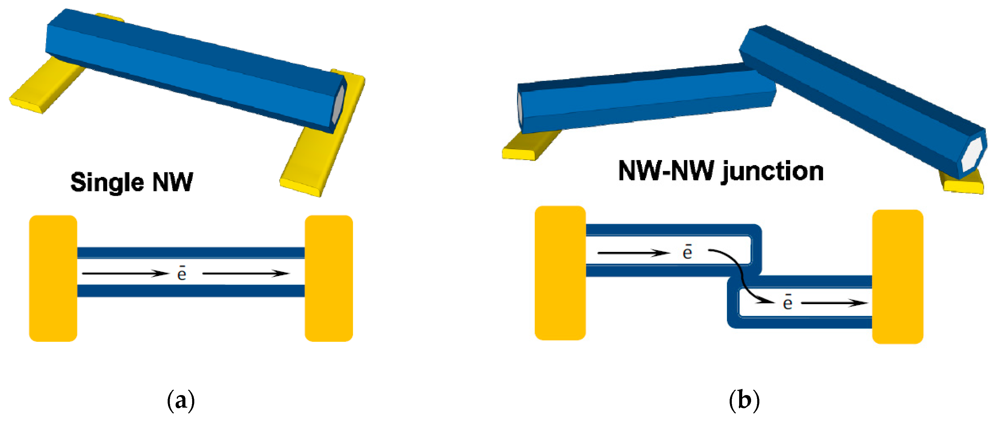
According to the device structure and working principle, nanowire sensors can be divided into two types: single nanowire connection and nanowire-nanowire junctions (Figure 2). Single connection devices rely on the response of a single NW, deposited or aligned between two metal contacts. Ohmic contacts are mostly used to contact ZnO NW; however, it is also possible to make Schottky contacts (e.g., contacting with Pt) in order to obtain a rectifying character or conduction [35]. However, most of research is done with NW-NW junction type of contacts, which is used not only because of the ease of sensor manufacture, but also due to the ability to control the barrier height. NW-NW junction sensors are typically more sensitive to small concentration changes, and have high rates of response as the conduction path involves tunneling through the depletion layer (Figure 2) [15]; however, in principle, single NW sensors can cover higher concentration ranges. Moreover, NW-NW junction integration into gas sensing devices is much more simple, as it relies on the randomly built conduction path between multiple NWs [15], whereas for the single NW sensors at least some degree of orientation is needed, wherefore ability to manipulate the NW or contacts is preferred [36].
Selectivity is another important feature of the ZnO NW sensors, which is connected to the ability of the sensor to discriminate among different types of chemical species. While, in biosensors, different analytes can be targeted with a special biomolecule, it is an especially difficult task to differentiate among the same type of gases (oxidizing or reducing), since depletion layer width change and consequently response will be in the same direction. Selective recognition of the gases can be addressed by variations in chemical adsorption and dissociation of the target gases at the NW surface; therefore, NW sensor selectivity can be approached by several methods: NW geometry control [36,37], NW functionalization [38,39], selective contact formation [40], heterojunction [41], operating temperature modulation [42], and sensor array formation [43].
2.1. ZnO NW Heterojunction
Heterojunction formation on ZnO NW, or simply a junction with other material, is mainly targeted to improve response and selectivity. A common choice for heterojunction is the use of metal oxides such as SnO2, because of high sensitivity. It was shown that ZnO NWs uniformly covered with the outer layer of n-type SnO2 nanoparticles [41] considerably improved the sensor response. Comparison of the gas sensor performance between SnO2, ZnO NW and the formed SnO2/ZnO NW heterojunction showed that, after functionalization, SnO2/ZnO NW sensor was responding at a high rate, selectivity and repeatability to n-butylamine gas was good, and therefore it can be applied for organic amine sensors. Another study used SnO2 NWs growth on ZnO NW for volatile organic compound sensing [44]. Advantageous sensor performance comparing to the pure ZnO NWs was explained by potential barriers, which were forming at the SnO2/ZnO. Moreover, the geometry of SnO2 nanowires affects the selectivity of triethylamine, toluene, ethanol, acetic acid, acetone, and methanol, allowing ZnO/SnO2 heterostructures to discriminate acetone from other volatile compounds.
Another option is to use ZnO NW heterojunction with p-type materials, forming local p-n junctions. Park et al. studied ZnO NW junction with CuO NW, by growing long crystalline nanowires and forming air-bridge-structured junction [45]. It was shown that formation of nanoscale p-n junctions lowers sensor conductance by two orders of magnitude (Figure 3). The current-voltage I-V characteristics of both ZnO NW and CuO NW contacts were symmetric, while ZnO/CuO NW heterocontacts were asymmetric, which indicate the built-in potential established near the p-n junction. P-type material plays the role of catalyst and expands the adjacent electron depletion layer of ZnO NWs. However, sensitivity toward H2, CO and NO2 gases was lower of such p-n heterocontacts than n-n contact between ZnO NWs.
Zhang et al. reported an increased sensitivity of ZnO NW with co-precipitated p-type CuO flower-type structure for ethanol vapor sensors [46]. The ZnO/uO heterojunction demonstrates 2.5 times higher ethanol response at 300 °C compared to ZnO NWs without CuO. Good selectivity, long-term stability and also response and recovery time of 7 and 9 s, respectively, were demonstrated. The improved ethanol response was also due to a widening of depletion layer on the ZnO/CuO interface.
In order to make a p-n heterojunction with ZnO NWs it is also possible to use other p type metal oxides, such as NiO [47,48], Cr2O3 [49,50], Mn3O4 [51] or modify with p-typematerials, such as cobalt phthalocyanine (CoPc) [52].
UV sensor performance can also be enhanced applying ZnO NW heterojunctions with p type oxides such as CuO [53] or NiO [54]. Ultrafast response to UV in µs range was obtained at ZnO NW contact with p-Si [55], which was explained by pyro-phototronic effect [56]. The pyro-phototronic results are from three elements: pyroelectric effect, photonic excitations, and semiconductor properties, the coupling of which paves a way to reach ultrafast photosensing performance with optoelectronic processes. Moreover, the response time of ZnO NW UV sensors decreases with increasing illumination intensity; thus, this could be potentially applied for ultrafast detection of intensive light.
Another interesting option is to decorate ZnO with noble metal particles. Metal nanoparticles can be employed to improve optical absorbance or emission in semiconductors, due to a high plasmon interaction with electromagnetic fields. ZnO NW gas sensing of ethanol can be improved by adding noble metallic nanoparticles, for example Au, Pt [57] or Ag [58]. Alternatively, a selective Pd contact with ZnO NWs [40] can be used for various gases such as H2, CH4, H2S and CO2 at different operating temperatures, where high efficiency in hydrogen detection was reported. Moreover, Pt contacted ZnO NW networks can be used as self-powered UV sensors, since excellent photoresponse properties to 365 nm UV irradiation was obtained at zero bias [31].
Combination of UV and Gas Sensing in ZnO NW
The high operating temperatures (typically about 350 °C) are essential for gas detection and sensing, which is a major technical limitation in applicability. Moreover, adsorption of water on the ZnO surface leads to a decrease in surface potential, at relative humidity higher than 14% due to adsorbed water molecules increasing the surface electron density [59]. Irradiation of ZnO by photons with an energy greater than the band gap (3.37 eV) changes adsorbed oxygen species on the surface, which is a practical alternative for achieving chemical reactions without the necessary heating. However, the UV activation shows an order of magnitude lower sensitivity compared to the same sensors activated by traditional heating methods [60]. UV activation, in order to increase the response, is used for ZnO films [59,61] and also for other materials [62,63]. A transparent ZnO NW sensor, which detects both UV and ethanol gas, was fabricated and deposited onto a silicon solar cell [64]. In UV sensing, the current rise was obtained in 137 s. In ethanol vapor detection, UV was used for sensitivity improvement. The ZnO NW sensor response increased by 13% with an ethanol gas concentration change of 100 ppm at 53 °C (heat generated by the c-Si solar cell). The sensor response is approximately zero without solar illumination.
Combining the response to chemical substance with a UV illumination, it is possible to get a synergy of these two effects and an increase of the performance of ZnO NW sensors (Figure 4); however, there are still only some studies on the combination of more than two effects on the performance of NW sensors. Synergistic effects of Cr2O3 functionalized ZnO NW sensor with UV irradiation were demonstrated for the ethanol gas sensing [65]. The responses at room temperature to ethanol were increased by UV illumination by 3.8 times for the pristine and by 7.7 times for Cr2O3 functionalized ZnO NW sensors. Moreover, the Cr2O3 modified ZnO NW sensor demonstrated rapid response and recovery; moreover, selectivity was also increased. This shows that combining heterostructures with UV activation has a synergistic effect on sensor performance. The synergistic effects arise from the Cr2O3 catalytic oxidation of ethanol and also from conduction channel width change due to Cr2O3 nanoparticle effect on ethanol adsorption and desorption under UV illumination in the Cr2O3 modified ZnO NW sensor.
Similarly, gold-decorated ZnO thin films showed improved sensing properties compared to bare ZnO under UV illumination. The sensor showed a selective response to NO2 gas under green light illumination. Moreover, Au/ZnO sensor can detect SO2 gas in ppm level in humid conditions [66].
2.2. ZnO Nanowire Biosensors
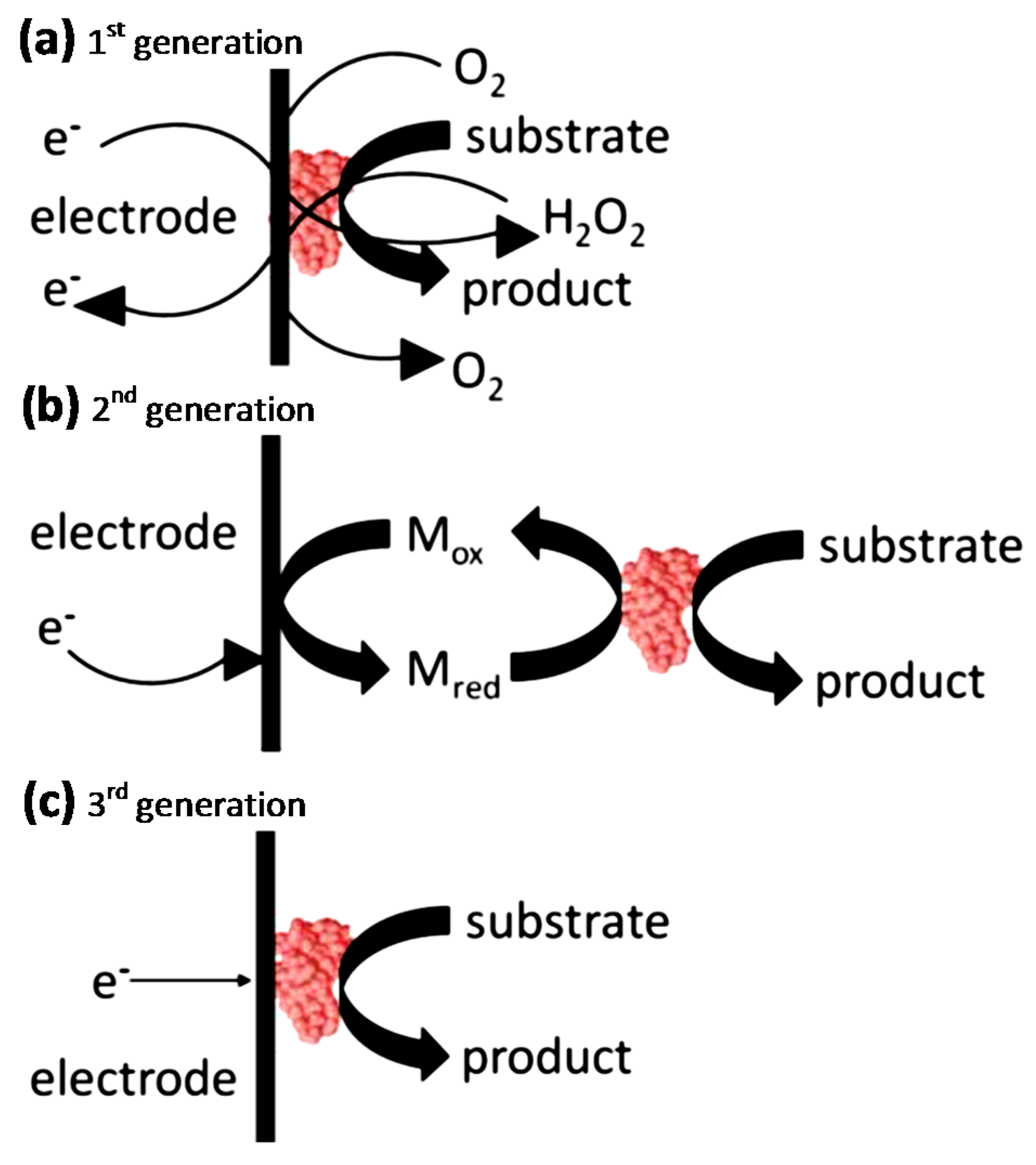
We can identify three generations of biosensors [67]. In the first generation (Figure 5a), an electrical response is generated by the diffusion of the reaction products to the transducer. In the second generation (Figure 5b), instead, an initial redox reaction is performed by a mediator between the enzyme and its substrate. The enzyme and mediator are usually co-immobilized at an electrode surface in the third-generation of biosensors (Figure 5c); in this way, the biorecognition component is an integral part of the electrode transducer [68].
Electronic devices based on semiconductor NW have emerged as a potential platform for the qualitative and quantitative detection of chemical and biological species due to their ultralow detection limit, fast readout and easy fabrication [70].
In particular, ZnO possesses a series of properties and characteristics (high electron mobility, easiness of fabrication of ZnO, biocompatibility and low toxicity) that makes it a nice candidate for the construction of biosensors [71]. In particular, ZnO NWs, due to their low weight with extraordinary mechanical, electrical, thermal and multifunctional properties along with their high surface area, are suitable for adsorption or immobilization of various biomolecules such as proteins, enzymes or antibodies [9]. ZnO nanowires possess active surfaces that can be modified for the immobilization of a large number of biomolecules. These nanostructures can be perfect transducers for producing signals to interface with macroscopic instruments since they present diameters which are comparable to the sizes of the biological and chemical species being sensed [72]. Based on the specific feature of NW, biosensors may even go down to a single molecule detection [73].
Qualitative and quantitative detection of chemical and biological species is crucial in a huge variety of fields. If the literature on biosensors based on ZnO nanomaterials is quite rich, relatively few examples are focused on ZnO nanowires. Below, we will briefly summarize some recent findings reporting biosensors based on ZnO nanowires.
2.2.1. Urea Biosensors
The importance of urea measurements in blood and serum is important for a certain number of diseases. ZnO nanomaterials comprising nanorods and nanowires have been used for the fabrication of urea biosensors [9]. Well-aligned ZnO NW arrays were fabricated on gold-coated plastic substrates by using a low-temperature aqueous chemical growth (ACG) method and were proved to be sensitive to urea detection at a concentration from 0.1 to 100 mM [74]. Urease was immobilized on the surface of the ZnO NWs using an electrostatic process. More recently, high quality ZnO NWs, synthesized by the chemical vapor deposition (CVD) method, were used for the fabrication of electrical biosensors based on field effect transistor (FET) for the simultaneously low and high concentrations detection of uric acid [73]. The obtained ZnO NW bioFET sensors could easily detect uric acid down to a concentration of 1 pM with 14.7 nS of conductance increase, and the response time turns out to be in the order of milliseconds.
2.2.2. Glucose Biosensors
Glucose is a critical metabolite for living organisms, particularly for patients who are suffering from diabetes, and glucose sensors attracted a huge amount of interest being one of the most important sensing technologies in medical science, clinical diagnostics, and food industry [75].
High-density vertical ZnO NWs were synthesized using the vapor-phase deposition method on patterned Au/glass electrode substrate with and without Au nanoparticle (NP) modification. A huge enhancement of the sensitivity toward glucose was obtained with Au NP modification [76]. A similar approach has been followed for the fabrication of high density, well-aligned ZnO NWs decorated with Pt nanoparticles to fabricate the working electrode for a non-enzymatic glucose biosensor [77]. ZnO NWs were synthesized hydrothermally on a glass substrate. The Pt NPs decoration allowed to enhance the biosensor’s glucose sensitivity 10-fold in comparison with the pristine ZnO NWs electrode. The large specific surface area, abundant microspace, small channels, and high isoelectric point (IEP) fracture of ZnO enable effective fluid circulation and good biocompatibility boding well for immobilization of enzymes. These characteristics were exploited for the immobilization of glucose oxidase on a glucose enzymatic biosensor composed of ZnO NWs supported by silicon NWs (ZnO/Si NWs) [78]. A Si NWs/ZnO nanowire nanocomposites enzymatic biosensor exhibited very strong and sensitive amperometric responses to glucose, even in the presence of common interfering species, and showed a high sensitivity of 129 μA·mM−1, low detection limit of 12 μΜ, and good stability as well as reproducibility. Very recently, a roll-to-roll flexographic printing technique was used for the fabrication of a three electrode electrochemical enzymatic biosensor consisting of ZnO NWs [79]. This biosensor device showed a typical sensitivity of 1.2 ± 0.2 μA·mM−1·cm−2 with a linear response to the addition of glucose over a concentration range of 0.1 to 3.6 mM.
2.2.3. DNA Detection
Nanomaterials can provide good opportunities for sequence-specific target DNA detection as a medium for signal amplification. The possibility of using ZnO NWs to fabricate electrochemical DNA biosensors was explored some years ago. In order to improve the sensitivity, multi-walled carbon nanotubes (MWCNTs) and gold nanoparticles (Au NPs) were employed. The resulting device was able to quantitatively detect target DNA from 1.0 × 10⁻⁷ to 1.0 × 10⁻¹³ M with a detection limit of 3.5 × 10⁻¹⁴ M [80]. Another ZnO NWs/Au electrode showed to be a suitable platform for the immobilization of DNA for the rapid detection of a sequence specific for the breast cancer 1 (BRCA1) gene [81]. This DNA biosensor has the ability to detect the target sequence in the range of concentration between 10.0 and 100.0 μM with a detection limit of 3.32 μM. A further sensitive and in situ selective label-free DNA sensor, based on a Schottky contacted ZnO NW device, has been fabricated. The performance of this device was significantly enhanced by the presence of piezotronic effect [82].
3. Conclusions
There is a growing interest in ZnO NW application for sensing due to their high temperature stability, biocompatibility, simple synthesis route and sensor manufacture. In this review, we have summarized recent strategies to enhance ZnO NW sensor performance. Several conclusions could be made with the proposal for future trends:
- Many synthetic routes for ZnO NWs are already found, and different ZnO NW structures can be obtained by varying growth conditions. Decoration with metal particles is easily achieved; however, there is still a lack of comparative studies where the sensor performance is related not to the synthesis conditions but to the morphology of the sensor, namely the size of a conductive channel and how it is influenced by absorbed material.
- Heterojunction brings another possibility for the improvement of the sensing which can be achieved with comparingly facile fabrication techniques. Junctions with other p or n materials can be made with controlled surface coverage and thickness; still, there is a need to optimize ZnO NW interface with other materials in order to obtain high efficiency sensing.
- Using UV activation for bio and chemoresistive sensors shows considerable improvement in sensing. However, there is still a lack of understanding for the interplay of several effects (UV, temperature, oxygen adsorption, etc.), especially at the junctions of NW to NW or p-n junctions.
- The unique properties of ZnO NWs, simple fabrication and the possibility for suitable surface functionalization of the NWs make them exemplar as biosensor materials for a great variety of applications.
- The devices can be fabricated by roll-to-roll printing, which is suitable for low-cost high-volume production and a spread of large-scale commercialization of the biosensors.
Acknowledgments
The work has received funding from the European Union’s Seventh Framework programme for research and innovation under the Marie Sklodowska-Curie grant agreement No 609402–2020 researchers: Train to Move (T2M).
Author Contributions
Simas Rackauskas worked on the ZnO nanowire sensors paragraphs while Nadia Barbero conceived and drafted the biosensor part. Claudia Barolo and Guido Viscardi coordinated and supervised the project. All authors analyzed and approved the final version of the manuscript.
Conflicts of Interest
The authors declare no conflict of interest.
References
- Zhang, Y. ZnO Nanostructures; Royal Society of Chemistry: Cambridge, UK, 2017; ISBN 978-1-78262-741-8. [Google Scholar]
- Kołodziejczak-Radzimska, A.; Jesionowski, T. Zinc Oxide—From synthesis to application: A review. Materials 2014, 7, 2833–2881. [Google Scholar] [CrossRef] [PubMed]
- Kaps, S.; Bhowmick, S.; Gröttrup, J.; Hrkac, V.; Stauffer, D.; Guo, H.; Warren, O.L.; Adam, J.; Kienle, L.; Minor, A.M.; et al. Piezoresistive response of quasi-one-dimensional ZnO nanowires using an In Situ electromechanical device. ACS Omega 2017, 2, 2985–2993. [Google Scholar] [CrossRef]
- Chu, S.; Wang, G.; Zhou, W.; Lin, Y.; Chernyak, L.; Zhao, J.; Kong, J.; Li, L.; Ren, J.; Liu, J. Electrically pumped waveguide lasing from ZnO nanowires. Nat. Nanotechnol. 2011, 6, 506–510. [Google Scholar] [CrossRef] [PubMed]
- Soci, C.; Zhang, A.; Xiang, B.; Dayeh, S.A.; Aplin, D.P.R.; Park, J.; Bao, X.Y.; Lo, Y.H.; Wang, D. ZnO nanowire UV photodetectors with high internal gain. Nano Lett. 2007, 7, 1003–1009. [Google Scholar] [CrossRef] [PubMed]
- Rackauskas, S.; Barbero, N.; Barolo, C.; Viscardi, G. ZnO nanowires for dye sensitized solar cells. In Nanowires—New Insights; InTech: Rijeka, Croatia, 2017. [Google Scholar]
- Znajdek, K.; Sibiński, M.; Lisik, Z.; Apostoluk, A.; Zhu, Y.; Masenelli, B.; Sędzicki, P. Zinc oxide nanoparticles for improvement of thin film photovoltaic structures’ efficiency through down shifting conversion. Opto-Electron. Rev. 2017, 25, 99–102. [Google Scholar] [CrossRef]
- Zhang, X.M.; Lu, M.Y.; Zhang, Y.; Chen, L.J.; Wang, Z.L. Fabrication of a high-brightness blue-light-emitting diode using a ZnO-Nanowire array grown on p-GaN thin film. Adv. Mater. 2009, 21, 2767–2770. [Google Scholar] [CrossRef]
- Zhang, Y.; Nayak, T.R.; Hong, H.; Cai, W. Biomedical applications of zinc oxide nanomaterials. Curr. Mol. Med. 2013, 13, 1633–1645. [Google Scholar] [CrossRef] [PubMed]
- Rackauskas, S.; Nasibulin, A.G.; Jiang, H.; Tian, Y.; Statkute, G.; Shandakov, S.D.; Lipsanen, H.; Kauppinen, E.I. Mechanistic investigation of ZnO nanowire growth. Appl. Phys. Lett. 2009, 95, 183114. [Google Scholar] [CrossRef]
- Rokhsat, E.; Akhavan, O. Improving the photocatalytic activity of graphene oxide/ZnO nanorod films by UV irradiation. Appl. Surf. Sci. 2016, 371, 592–595. [Google Scholar] [CrossRef]
- Tarat, A.; Majithia, R.; Brown, R.A.; Penny, M.W.; Meissner, K.E.; Maffeis, T.G.G. Synthesis of nanocrystalline ZnO nanobelts via pyrolytic decomposition of zinc acetate nanobelts and their gas sensing behavior. Surf. Sci. 2012, 606, 715–721. [Google Scholar] [CrossRef]
- Ko, S.H.; Lee, D.; Kang, H.W.; Nam, K.H.; Yeo, J.Y.; Hong, S.J.; Grigoropoulos, C.P.; Sung, H.J. Nanoforest of hydrothermally grown hierarchical ZnO nanowires for a high efficiency dye-sensitized solar cell. Nano Lett. 2011, 11, 666–671. [Google Scholar] [CrossRef] [PubMed]
- Rackauskas, S.; Klimova, O.; Jiang, H.; Nikitenko, A.; Chernenko, K.A.; Shandakov, S.D.; Kauppinen, E.I.; Tolochko, O.V.; Nasibulin, A.G. A novel method for continuous synthesis of ZnO tetrapods. J. Phys. Chem. C 2015, 119, 16366–16373. [Google Scholar] [CrossRef]
- Rackauskas, S.; Mustonen, K.; Järvinen, T.; Mattila, M.; Klimova, O.; Jiang, H.; Tolochko, O.; Lipsanen, H.; Kauppinen, E.I.; Nasibulin, A.G. Synthesis of ZnO tetrapods for flexible and transparent UV sensors. Nanotechnology 2012, 23, 95502. [Google Scholar] [CrossRef] [PubMed]
- Mishra, Y.K.; Modi, G.; Cretu, V.; Postica, V.; Lupan, O.; Reimer, T.; Paulowicz, I.; Hrkac, V.; Benecke, W.; Kienle, L.; et al. Direct growth of freestanding ZnO tetrapod networks for multifunctional applications in photocatalysis, UV photodetection, and gas sensing. ACS Appl. Mater. Interfaces 2015, 7, 14303–14316. [Google Scholar] [CrossRef] [PubMed]
- Gedamu, D.; Paulowicz, I.; Kaps, S.; Lupan, O.; Wille, S.; Haidarschin, G.; Mishra, Y.K.; Adelung, R. Rapid fabrication technique for interpenetrated ZnO nanotetrapod networks for fast UV sensors. Adv. Mater. 2014, 26, 1541–1550. [Google Scholar] [CrossRef] [PubMed]
- Bielinski, A.R.; Kazyak, E.; Schlepütz, C.M.; Jung, H.J.; Wood, K.N.; Dasgupta, N.P. Hierarchical ZnO nanowire growth with tunable orientations on versatile substrates using atomic layer deposition seeding. Chem. Mater. 2015, 27, 4799–4807. [Google Scholar] [CrossRef]
- Pugliese, D.; Bella, F.; Cauda, V.; Lamberti, A.; Sacco, A.; Tresso, E.; Bianco, S. A chemometric approach for the sensitization procedure of ZnO flowerlike microstructures for dye-sensitized solar cells. ACS Appl. Mater. Interfaces 2013, 5, 11288–11295. [Google Scholar] [CrossRef] [PubMed]
- Kuo, S.-Y.; Yang, J.-F.; Lai, F.-I. Improved dye-sensitized solar cell with a ZnO nanotree photoanode by hydrothermal method. Nanoscale Res. Lett. 2014, 9, 206. [Google Scholar] [CrossRef] [PubMed]
- Zhang, S.; Chen, H.-S.; Matras-Postolek, K.; Yang, P. ZnO nanoflowers with single crystal structure towards enhanced gas sensing and photocatalysis. Phys. Chem. Chem. Phys. 2015, 17, 30300–30306. [Google Scholar] [CrossRef] [PubMed]
- Lu, C.; Qi, L.; Yang, J.; Tang, L.; Zhang, D.; Ma, J. Hydrothermal growth of large-scale micropatterned arrays of ultralong ZnO nanowires and nanobelts on zinc substrate. Chem. Commun. 2006, 432, 3551–3553. [Google Scholar] [CrossRef] [PubMed]
- Baruah, S.; Dutta, J. Hydrothermal growth of ZnO nanostructures. Sci. Technol. Adv. Mater. 2009, 10, 013001. [Google Scholar] [CrossRef] [PubMed]
- Bae, S.Y.; Seo, H.W.; Park, J. Vertically aligned sulfur-doped ZnO nanowires synthesized via chemical vapor deposition. J. Phys. Chem. B 2004, 108, 5206–5210. [Google Scholar] [CrossRef]
- Kuo, T.J.; Lin, C.N.; Kuo, C.L.; Huang, M.H. Growth of ultralong ZnO nanowires on silicon substrates by vapor transport and their use as recyclable photocatalysts. Chem. Mater. 2007, 19, 5143–5147. [Google Scholar] [CrossRef]
- Rackauskas, S.; Nasibulin, A.G.; Jiang, H.; Tian, Y.; Kleshch, V.I.; Sainio, J.; Obraztsova, E.D.; Bokova, S.N.; Obraztsov, A.N.; Kauppinen, E.I. A novel method for metal oxide nanowire synthesis. Nanotechnology 2009, 20, 165603. [Google Scholar] [CrossRef] [PubMed]
- Kleshch, V.I.; Rackauskas, S.; Nasibulin, A.G.; Kauppinen, E.I.; Obraztsova, E.D.; Obraztsov, A.N. Field emission properties of metal oxide nanowires. J. Nanoelectron. Optoelectron. 2012, 7, 35–40. [Google Scholar] [CrossRef]
- Choi, K.J.; Jang, H.W. One-dimensional oxide nanostructures as gas-sensing materials: Review and issues. Sensors 2010, 10, 4083–4099. [Google Scholar] [CrossRef] [PubMed]
- Lupan, O.; Cretu, V.; Postica, V.; Ababii, N.; Polonskyi, O.; Kaidas, V.; Schütt, F.; Mishra, Y.K.; Monaico, E.; Tiginyanu, I.; et al. Enhanced ethanol vapour sensing performances of copper oxide nanocrystals with mixed phases. Sens. Actuators B 2016, 224, 434–448. [Google Scholar] [CrossRef]
- Paulowicz, I.; Hrkac, V.; Kaps, S.; Cretu, V.; Lupan, O.; Braniste, T.; Duppel, V.; Tiginyanu, I.; Kienle, L.; Adelung, R.; et al. Three-dimensional SnO2 nanowire networks for multifunctional applications: From high-temperature stretchable ceramics to ultraresponsive sensors. Adv. Electron. Mater. 2015, 1, 1500081. [Google Scholar] [CrossRef]
- Bai, Z.; Yan, X.; Chen, X.; Zhao, K.; Lin, P.; Zhang, Y. High sensitivity, fast speed and self-powered ultraviolet photodetectors based on ZnO micro/nanowire networks. Prog. Nat. Sci. 2014, 24, 1–5. [Google Scholar] [CrossRef]
- Lu, M.-P.; Lu, M.-Y.; Chen, L.-J. p-Type ZnO nanowires: From synthesis to nanoenergy. Nano Energy 2012, 1, 247–258. [Google Scholar] [CrossRef]
- Yuan, G.D.; Zhang, W.J.; Jie, J.S.; Fan, X.; Zapien, J.A.; Leung, Y.H.; Luo, L.B.; Wang, P.F.; Lee, C.S.; Lee, S.T. p-type ZnO nanowire arrays. Nano Lett. 2008, 8, 2591–2597. [Google Scholar] [CrossRef] [PubMed]
- Chen, J.; Wang, K.; Cao, B.; Zhou, W. Highly sensitive and selective gas detection by 3D metal oxide nanoarchitectures. In Three-Dimensional Nanoarchitectures; Springer: New York, NY, USA, 2011; pp. 391–412. ISBN 978-1-4419-9822-4. [Google Scholar]
- Bercu, B.; Geng, W.; Simonetti, O.; Kostcheev, S.; Sartel, C.; Sallet, V.; Lérondel, G.; Molinari, M.; Giraudet, L.; Couteau, C. Characterizations of Ohmic and Schottky-behaving contacts of a single ZnO nanowire. Nanotechnology 2013, 24, 415202. [Google Scholar] [CrossRef] [PubMed]
- Schütt, F.; Postica, V.; Adelung, R.; Lupan, O. Single and networked ZnO–CNT hybrid tetrapods for selective room-temperature high-performance ammonia sensors. ACS Appl. Mater. Interfaces 2017, 9, 23107–23118. [Google Scholar] [CrossRef] [PubMed]
- Sysoev, V.V.; Strelcov, E.; Sommer, M.; Bruns, M.; Kiselev, I.; Habicht, W.; Kar, S.; Gregoratti, L.; Kiskinova, M.; Kolmakov, A. Single-nanobelt electronic nose: Engineering and tests of the simplest analytical element. ACS Nano 2010, 4, 4487–4494. [Google Scholar] [CrossRef] [PubMed]
- Lupan, O.; Postica, V.; Gröttrup, J.; Mishra, A.K.; de Leeuw, N.H.; Carreira, J.F.C.; Rodrigues, J.; Ben Sedrine, N.; Correia, M.R.; Monteiro, T.; et al. Hybridization of Zinc oxide tetrapods for selective gas sensing applications. ACS Appl. Mater. Interfaces 2017, 9, 4084–4099. [Google Scholar] [CrossRef] [PubMed]
- Sun, G.-J.; Lee, J.K.; Choi, S.; Lee, W.I.; Kim, H.W.; Lee, C. Selective oxidizing gas sensing and dominant sensing mechanism of n-CaO-decorated n-ZnO nanorod sensors. ACS Appl. Mater. Interfaces 2017, 9, 9975–9985. [Google Scholar] [CrossRef] [PubMed]
- Kumar, M.; Singh Bhati, V.; Ranwa, S.; Singh, J.; kumar, M. Pd/ZnO nanorods based sensor for highly selective detection of extremely low concentration hydrogen. Sci. Rep. 2017, 7, 236. [Google Scholar] [CrossRef] [PubMed]
- Wang, L.; Li, J.; Wang, Y.; Yu, K.; Tang, X.; Zhang, Y.; Wang, S.; Wei, C. Construction of 1D SnO2-coated ZnO nanowire heterojunction for their improved n-butylamine sensing performances. Sci. Rep. 2016, 6, 35079. [Google Scholar] [CrossRef] [PubMed]
- Li, F.-A.; Jin, H.; Wang, J.; Zou, J.; Jian, J. Selective sensing of gas mixture via a temperature modulation approach: New strategy for potentiometric gas sensor obtaining satisfactory discriminating features. Sensors 2017, 17, 573. [Google Scholar] [CrossRef] [PubMed]
- Fedorov, F.; Vasilkov, M.; Lashkov, A.; Varezhnikov, A.; Fuchs, D.; Kübel, C.; Bruns, M.; Sommer, M.; Sysoev, V. Toward new gas-analytical multisensor chips based on titanium oxide nanotube array. Sci. Rep. 2017, 7, 9732. [Google Scholar] [CrossRef] [PubMed]
- Rakshit, T.; Santra, S.; Manna, I.; Ray, S.K. Enhanced sensitivity and selectivity of brush-like SnO2 nanowire/ZnO nanorod heterostructure based sensors for volatile organic compounds. RSC Adv. 2014, 4, 36749–36756. [Google Scholar] [CrossRef]
- Park, W.J.; Choi, K.J.; Kim, M.H.; Koo, B.H.; Lee, J.-L.; Baik, J.M. Self-assembled and highly selective sensors based on air-bridge-structured nanowire junction arrays. ACS Appl. Mater. Interfaces 2013, 5, 6802–6807. [Google Scholar] [CrossRef] [PubMed]
- Zhang, Y.-B.; Yin, J.; Li, L.; Zhang, L.-X.; Bie, L.-J. Enhanced ethanol gas-sensing properties of flower-like p-CuO/n-ZnO heterojunction nanorods. Sens. Actuators B 2014, 202, 500–507. [Google Scholar] [CrossRef]
- Ju, D.; Xu, H.; Qiu, Z.; Guo, J.; Zhang, J.; Cao, B. Highly sensitive and selective triethylamine-sensing properties of nanosheets directly grown on ceramic tube by forming NiO/ZnO PN heterojunction. Sens. Actuators B 2014, 200, 288–296. [Google Scholar] [CrossRef]
- Na, C.W.; Woo, H.-S.; Lee, J.-H.; Yao, P.J.; Nishibori, M.; Wang, D.; Wang, C.; Pinna, N.; Lee, J.H. Design of highly sensitive volatile organic compound sensors by controlling NiO loading on ZnO nanowire networks. RSC Adv. 2012, 2, 414–417. [Google Scholar] [CrossRef]
- Woo, H.-S.; Na, C.W.; Kim, I.-D.; Lee, J.-H. Highly sensitive and selective trimethylamine sensor using one-dimensional ZnO–Cr2O3 hetero-nanostructures. Nanotechnology 2012, 23, 245501. [Google Scholar] [CrossRef] [PubMed]
- Park, S.; Kim, S.; Kheel, H.; Lee, C. Oxidizing gas sensing properties of the n-ZnO/p-Co3O4 composite nanoparticle network sensor. Sens. Actuators B 2015, 222, 1193–1200. [Google Scholar] [CrossRef]
- Na, C.W.; Park, S.Y.; Chung, J.H.; Lee, J.H. Transformation of ZnO nanobelts into single-crystalline Mn3O4 nanowires. ACS Appl. Mater. Interfaces 2012, 4, 6565–6572. [Google Scholar] [CrossRef] [PubMed]
- Kumar, A.; Samanta, S.; Singh, A.; Roy, M.; Singh, S.; Basu, S.; Chehimi, M.M.; Roy, K.; Ramgir, N.; Navaneethan, M.; et al. Fast response and high sensitivity of ZnO nanowires-cobalt phthalocyanine heterojunction based H2S sensor. ACS Appl Mater. Interfaces 2015, 7, 17713–17724. [Google Scholar] [CrossRef] [PubMed]
- Wu, J.-K.; Chen, W.-J.; Chang, Y.H.; Chen, Y.F.; Hang, D.-R.; Liang, C.-T.; Lu, J.-Y. Fabrication and photoresponse of ZnO nanowires/CuO coaxial heterojunction. Nanoscale Res. Lett. 2013, 8, 387. [Google Scholar] [CrossRef] [PubMed]
- Li, Y.-R.; Wan, C.-Y.; Chang, C.-T.; Tsai, W.-L.; Huang, Y.-C.; Wang, K.-Y.; Yang, P.-Y.; Cheng, H.-C. Thickness effect of NiO on the performance of ultraviolet sensors with p-NiO/n-ZnO nanowire heterojunction structure. Vacuum 2015, 118, 48–54. [Google Scholar] [CrossRef]
- Wang, Z.; Yu, R.; Wang, X.; Wu, W.; Wang, Z.L. Ultrafast response p-Si/n-ZnO heterojunction ultraviolet detector based on pyro-phototronic effect. Adv. Mater. 2016, 28, 6880–6886. [Google Scholar] [CrossRef] [PubMed]
- Wang, Z.; Yu, R.; Pan, C.; Li, Z.; Yang, J.; Yi, F.; Wang, Z.L. Light-induced pyroelectric effect as an effective approach for ultrafast ultraviolet nanosensing. Nat. Commun. 2015, 6, 8401. [Google Scholar] [CrossRef] [PubMed]
- Liu, X.; Zhang, J.; Guo, X.; Wu, S.; Wang, S. Amino acid-assisted one-pot assembly of Au, Pt nanoparticles onto one-dimensional ZnO microrods. Nanoscale 2010, 2, 1178–1184. [Google Scholar] [CrossRef] [PubMed]
- Ding, J.; Zhu, J.; Yao, P.; Li, J.; Bi, H.; Wang, X. Synthesis of ZnO-Ag hybrids and their gas-sensing performance toward ethanol. Ind. Eng. Chem. Res. 2015, 54, 8947–8953. [Google Scholar] [CrossRef]
- Jacobs, C.B.; Maksov, A.B.; Muckley, E.S.; Collins, L.; Mahjouri-Samani, M.; Ievlev, A.; Rouleau, C.M.; Moon, J.-W.; Graham, D.E.; Sumpter, B.G.; et al. UV-activated ZnO films on a flexible substrate for room temperature O2 and H2O sensing. Sci. Rep. 2017, 7, 6053. [Google Scholar] [CrossRef] [PubMed]
- Alenezi, M.R.; Alshammari, A.S.; Jayawardena, K.D.G.I.; Beliatis, M.J.; Henley, S.J.; Silva, S.R.P. Role of the exposed polar facets in the performance of thermally and UV activated ZnO nanostructured gas sensors. J. Phys. Chem. C 2013, 117, 17850–17858. [Google Scholar] [CrossRef] [PubMed] [Green Version]
- Fan, S.-W.; Srivastava, A.K.; Dravid, V.P. UV-activated room-temperature gas sensing mechanism of polycrystalline ZnO. Appl. Phys. Lett. 2009, 95, 142106. [Google Scholar] [CrossRef]
- Comini, E.; Cristalli, A.; Faglia, G.; Sberveglieri, G. Light enhanced gas sensing properties of indium oxide and tin dioxide sensors. Sens. Actuators B 2000, 65, 260–263. [Google Scholar] [CrossRef]
- Gromova, Y.; Alaferdov, A.; Rackauskas, S.; Ermakov, V.; Orlova, A.; Maslov, V.; Moshkalev, S.; Baranov, A.; Fedorov, A. Photoinduced electrical response in quantum dots/graphene hybrid structure. J. Appl. Phys. 2015, 118, 104305. [Google Scholar] [CrossRef]
- Lin, C.H.; Chang, S.-J.J.; Chen, W.-S.; Hsueh, T.-J.J. Transparent ZnO-nanowire-based device for UV light detection and ethanol gas sensing on c-Si solar cell. RSC Adv. 2016, 6, 42–54. [Google Scholar] [CrossRef]
- Park, S.; Sun, G.-J.; Jin, C.; Kim, H.W.; Lee, S.; Lee, C. Synergistic effects of a combination of Cr2O3—Functionalization and UV-irradiation techniques on the ethanol gas sensing performance of ZnO nanorod gas sensors. ACS Appl. Mater. Interfaces 2016, 8, 2805–2811. [Google Scholar] [CrossRef] [PubMed]
- Gaiardo, A.; Fabbri, B.; Giberti, A.; Guidi, V.; Bellutti, P.; Malagu, C.; Valt, M.; Pepponi, G.; Gherardi, S.; Zonta, G.; et al. ZnO and Au/ZnO thin films: Room-temperature chemoresistive properties for gas sensing applications. Sens. Actuators B 2016, 237, 1085–1094. [Google Scholar] [CrossRef]
- Zhu, P.; Weng, Z.; Li, X.; Liu, X.; Wu, S.; Yeung, K.W.K.; Wang, X.; Cui, Z.; Yang, X.; Chu, P.K. Biomedical applications of functionalized ZnO nanomaterials: From biosensors to bioimaging. Adv. Mater. Interfaces 2016, 3, 1500494. [Google Scholar] [CrossRef]
- Ronkainen, N.J.; Halsall, H.B.; Heineman, W.R. Electrochemical biosensors. Chem. Soc. Rev. 2010, 39, 1747–1763. [Google Scholar] [CrossRef] [PubMed]
- Putzbach, W.; Ronkainen, N.J. Immobilization techniques in the fabrication of nanomaterial-based electrochemical biosensors: A review. Sensors 2013, 13, 4811–4840. [Google Scholar] [CrossRef] [PubMed]
- Zhu, C.; Yang, G.; Li, H.; Du, D.; Lin, Y. Electrochemical sensors and biosensors based on nanomaterials and nanostructures. Anal. Chem. 2015, 87, 230–249. [Google Scholar] [CrossRef] [PubMed]
- Xu, C.X.; Yang, C.; Gu, B.X.; Fang, S.J. Nanostructured ZnO for biosensing applications. Chin. Sci. Bull. 2013, 58, 2563–2566. [Google Scholar] [CrossRef]
- Choi, A.; Kim, K.; Jung, H.I.; Lee, S.Y. ZnO nanowire biosensors for detection of biomolecular interactions in enhancement mode. Sens. Actuators B 2010, 148, 577–582. [Google Scholar] [CrossRef]
- Liu, X.; Lin, P.; Yan, X.; Kang, Z.; Zhao, Y.; Lei, Y.; Li, C.; Du, H.; Zhang, Y. Enzyme-coated single ZnO nanowire FET biosensor for detection of uric acid. Sens. Actuators B 2013, 176, 22–27. [Google Scholar] [CrossRef]
- Ali, S.M.U.; Ibupoto, Z.H.; Salman, S.; Nur, O.; Willander, M.; Danielsson, B. Selective determination of urea using urease immobilized on ZnO nanowires. Sens. Actuators B 2011, 160, 637–643. [Google Scholar] [CrossRef]
- Yu, R.; Pan, C.; Chen, J.; Zhu, G.; Wang, Z.L. Enhanced performance of a ZnO nanowire-based self-powered glucose sensor by piezotronic effect. Adv. Funct. Mater. 2013, 23, 5868–5874. [Google Scholar] [CrossRef]
- Lin, S.Y.; Chang, S.J.; Hsueh, T.J. ZnO nanowires modified with Au nanoparticles for nonenzymatic amperometric sensing of glucose. Appl. Phys. Lett. 2014, 104, 193704. [Google Scholar] [CrossRef]
- Hsu, C.L.; Lin, J.H.; Hsu, D.X.; Wang, S.H.; Lin, S.Y.; Hsueh, T.J. Enhanced non-enzymatic glucose biosensor of ZnO nanowires via decorated Pt nanoparticles and illuminated with UV/green light emitting diodes. Sens. Actuators B 2017, 238, 150–159. [Google Scholar] [CrossRef]
- Miao, F.; Lu, X.; Tao, B.; Li, R.; Chu, P.K. Glucose oxidase immobilization platform based on ZnO nanowires supported by silicon nanowires for glucose biosensing. Microelectron. Eng. 2016, 149, 153–158. [Google Scholar] [CrossRef]
- Fung, C.M.; Lloyd, J.S.; Samavat, S.; Deganello, D.; Teng, K.S. Facile fabrication of electrochemical ZnO nanowire glucose biosensor using roll to roll printing technique. Sens. Actuators B 2017, 247, 807–813. [Google Scholar] [CrossRef]
- Wang, J.; Li, S.; Zhang, Y. A sensitive DNA biosensor fabricated from gold nanoparticles, carbon nanotubes, and zinc oxide nanowires on a glassy carbon electrode. Electrochim. Acta 2010, 55, 4436–4440. [Google Scholar] [CrossRef]
- Mansor, N.A.; Zain, Z.M.; Hamzah, H.H.; Noorden, M.S.A.; Jaapar, S.S.; Beni, V.; Ibupoto, Z.H. Detection of Breast Cancer 1 (BRCA1) gene using an electrochemical DNA biosensor based on immobilized ZnO nanowires. Open J. Appl. Biosens. 2014, 3, 9–17. [Google Scholar] [CrossRef]
- Cao, X.; Cao, X.; Guo, H.; Li, T.; Jie, Y.; Wang, N.; Wang, Z.L. Piezotronic effect enhanced label-free detection of DNA using a schottky-contacted ZnO nanowire biosensor. ACS Nano 2016, 10, 8038–8044. [Google Scholar] [CrossRef] [PubMed]
Figure 1.
Schematics of unified ZnO nanowire (NW) chemoresistive sensing principle, based on the depletion layer width change with absorption-desorption of oxygen.
Figure 1.
Schematics of unified ZnO nanowire (NW) chemoresistive sensing principle, based on the depletion layer width change with absorption-desorption of oxygen.
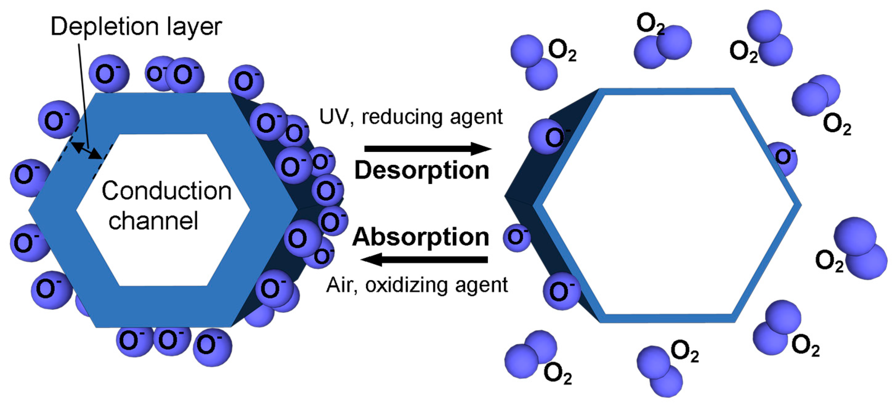
Figure 2.
Schematics of ZnO NW sensor geometry types: (a) single NW; (b) NW-NW junction.

Figure 3.
Comparison of contacts between ZnO and CuO NWs: (a) current-voltage (I-V) curves obtained at room temperature, demonstrating the characteristic nonlinear Schottky-like transport behavior; (b) Energy band diagram for every interconnection type between NWs. Reproduced with permission from [45]. Copyright American Chemical Society, 2013.
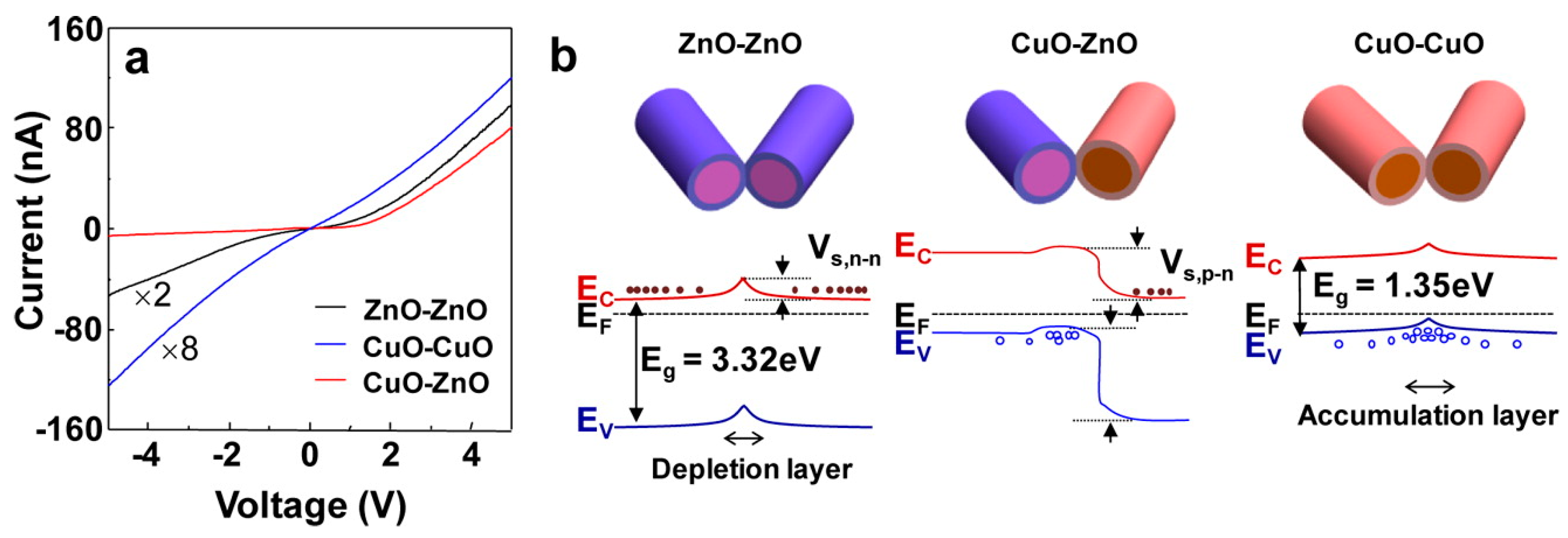
Figure 4.
Schematic diagrams: (a) pristine ZnO NW; (b) Cr2O3-modified ZnO NW in the dark and under UV illumination in air and ethanol showing the depletion layer and conduction path. Reproduced with permission from [65]. Copyright American Chemical Society, 2016.
Figure 4.
Schematic diagrams: (a) pristine ZnO NW; (b) Cr2O3-modified ZnO NW in the dark and under UV illumination in air and ethanol showing the depletion layer and conduction path. Reproduced with permission from [65]. Copyright American Chemical Society, 2016.
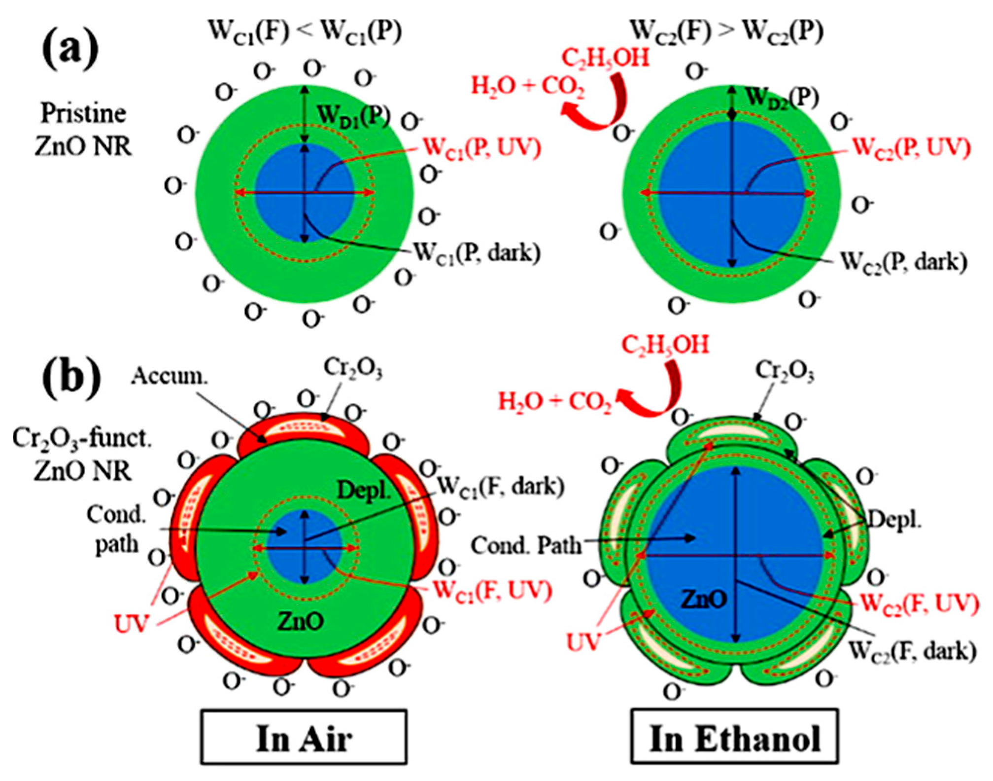
Figure 5.
Schematic diagrams of three generations of sensors: (a) 1st generation; (b) 2nd generation and (c) 3rd generation [69].
Figure 5.
Schematic diagrams of three generations of sensors: (a) 1st generation; (b) 2nd generation and (c) 3rd generation [69].

© 2017 by the authors. Licensee MDPI, Basel, Switzerland. This article is an open access article distributed under the terms and conditions of the Creative Commons Attribution (CC BY) license (http://creativecommons.org/licenses/by/4.0/).
Share and Cite
MDPI and ACS Style
Rackauskas, S.; Barbero, N.; Barolo, C.; Viscardi, G. ZnO Nanowire Application in Chemoresistive Sensing: A Review. Nanomaterials 2017, 7, 381. https://doi.org/10.3390/nano7110381
AMA Style
Rackauskas S, Barbero N, Barolo C, Viscardi G. ZnO Nanowire Application in Chemoresistive Sensing: A Review. Nanomaterials. 2017; 7(11):381. https://doi.org/10.3390/nano7110381
Chicago/Turabian StyleRackauskas, Simas, Nadia Barbero, Claudia Barolo, and Guido Viscardi. 2017. "ZnO Nanowire Application in Chemoresistive Sensing: A Review" Nanomaterials 7, no. 11: 381. https://doi.org/10.3390/nano7110381
Note that from the first issue of 2016, this journal uses article numbers instead of page numbers. See further details here.