Article

Comparison of Erosion Behavior and Particle Contamination in Mass-Production CF4/O2 Plasma Chambers Using Y2O3 and YF3 Protective Coatings

1
Department of Materials Science and Engineering, National Chung Hsing University, Taichung 40227, Taiwan
2
Department of Materials Science and Engineering, Da-Yeh University, Changhua 51591, Taiwan
3
Department of Industrial Engineering and Management, Da-Yeh University, Changhua 51591, Taiwan
4
Center for Advanced Industry Technology and Precision Processing, National Chung Hsing University, Taichung 40227, Taiwan
*
Author to whom correspondence should be addressed.
Nanomaterials 2017, 7(7), 183; https://doi.org/10.3390/nano7070183
Submission received: 15 June 2017 / Revised: 6 July 2017 / Accepted: 11 July 2017 / Published: 14 July 2017

Abstract

:
Yttrium fluoride (YF3) and yttrium oxide (Y2O3) protective coatings prepared using an atmospheric plasma spraying technique were used to investigate the relationship between surface erosion behaviors and their nanoparticle generation under high-density plasma (1012–1013 cm−3) etching. As examined by transmission electron microscopy, the Y2O3 and YF3 coatings become oxyfluorinated after exposure to the plasma, wherein the yttrium oxyfluoride film formation was observed on the surface with a thickness of 5.2 and 6.8 nm, respectively. The difference in the oxyfluorination of Y2O3 and YF3 coatings could be attributed to Y–F and Y–O bonding energies. X-ray photoelectron spectroscopy analyses revealed that a strongly fluorinated bonding (Y–F bond) was obtained on the etched surface of the YF3 coating. Scanning electron microscopy and energy dispersive X-ray diffraction analysis revealed that the nanoparticles on the 12-inch wafer are composed of etchant gases and Y2O3. These results indicate that the YF3 coating is a more erosion-resistant material, resulting in fewer contamination particles compared with the Y2O3 coating.

Graphical Abstract

1. Introduction

Silicon-based ceramics have been extensively used in semiconductor plasma processing equipment as plasma-facing materials, due to their hardness, high wear resistance, dielectric strength, high corrosion resistance, and chemical stability [1,2]. They are used mainly as a shield to protect the ceramic parts inside etchers or chemical vapor deposition reactor chambers from corrosion caused by fluorocarbon corrosive gases such as CF4, CHF3, C4F6, and C2F6 [3,4,5]. These materials interact with plasma and are eroded, resulting in the production of contaminant particles on the wafer. As integrated circuits continue to scale down with wider use of high-density plasma for wafer processing, the particles generated in the plasma processing equipment cause serious problems, such as short current in integration circuit and lower production yield [6,7]. In order to solve this problem, yttrium oxide (Y2O3) was adopted as plasma-facing inner wall materials in plasma processing equipment because their plasma erosion resistance values are much higher than those of conventional SiO2 coatings [8,9,10]. Mass-production factories have found that the Y2O3 inner walls have problems with significant erosion and particle generation [11]. Under fluorine-based plasma processing, a thin top carbonaceous polymer reaction layer has been identified depending on the etching conduction and the etched materials [12,13,14]. The polymer layer thickness is determined using polymer deposition and its removal rate, and consumption rate in substrate etching. This polymer layer etching rate is affected by the plasma incident ion kinetic energy. Some volatile etching products are produced during the etching process, such as carbon oxide, carbon oxyfluorides, and silicon fluorides [15]. Unlike silicon-based materials, the yttrium-based material etching mechanism is not fully understood. Yttrium fluoride (YF3) coatings ave recently attracted substantial attention because of their high plasma erosion resistance, preventing the generation of fluoride particles on the chamber wall surface, reducing particulate contamination [16]. Thus, the YF3 coating might be a new plasma-facing material that produces fewer contamination particles. The Y2O3 and YF3 coatings were deposited using atmospheric plasma spraying (APS). In this study, the mechanism of formation of yttrium oxyfluoride film and their particle trajectories in industrial plasma processing tools have been examined. Moreover, we compared the etching behavior of Y2O3 and YF3 coatings and their compounds under fluorocarbon plasma. The surface morphology, chemical reactions on the etched surface, microstructure, and particle contaminations of Y2O3 and YF3 coatings were investigated.

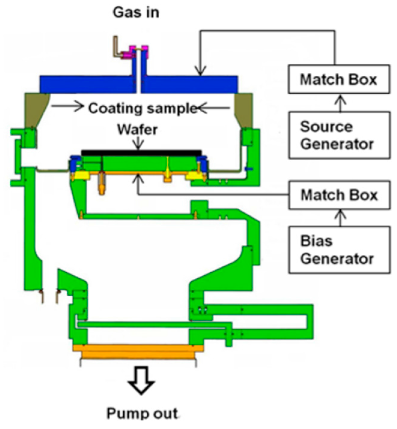
2. Materials and Methods

Commercially available YF3 powders (25–50 μm, 99.99%, Shin-Etsu Chemical, Tokyo, Japan) and Y2O3 powders (25–50 μm, 99.99%, Shin-Etsu Chemical, Tokyo, Japan) were used as the spraying materials. YF3 and Y2O3 coatings were prepared using APS with an F4-MB plasma gun (Sulzer Metco, Orelikon, Pfaeffikon, Switzerland). An alloy aluminum (A6061) substrate was used for the experiment. The specimen had a size of 400 mm2 and a thickness of 20 mm. Before APS, the substrate was treated with sandblasting. The sandblasting material was SiO2. Acetone was used to clean the substrate. The stand-off distance was adjusted to 10 cm. The Ar and H2 gas cylinders were opened when the air compressor was initiated. The Ar flow rate, H2 flow rate, system voltage, gun movement rate, and feed rate were set to 45 L/min, 6 L/min, 50 V, 10 cm/s, and 15 g/min, respectively. The YF3 and Y2O3 spraying parameters are shown in Table 1. The erosion behaviors of both protective coatings were performed using an inductively coupled plasma (ICP) etcher (LAM 2300 Metal) under the routine plasma etching process; i.e., the same bias power and processing gases (CF4 and O2). High-density CF4/O2 plasma with electron densities on the order of 1012 to 1013 cm−3 has been produced. Figure 1 shows a schematic diagram of the ICP etcher system employed in this study. The etch process details are shown in Table 2. Three-hundred millimeter blanket wafers with chemical vapor deposition titanium nitride layer/Si-substrate were prepared to evaluate the integrated circuit defective performance after dry etching process measured by Surfscan SP3 (Surfscan SP3, KLA-Tencor Corporation, Milpitas, CA, USA).
The surface morphology, microstructure, and elemental analysis of these coating samples were conducted using scanning electron microscopy (SEM, S-3000H, Hitachi, Tokyo, Japan) coupled with energy dispersive X-ray diffraction (EDX) and transmission electron microcopy (TEM, H-600, Hitachi, Tokyo, Japan). The composition of these samples were examined by X-ray photoelectron spectroscopy (XPS, PHI 5000 VersaProbe, ULVAC-PHI, Kanagawa, Japan) using a monochromatic Al Kα X-ray source at a passing energy of 20 eV with a spot size of 650 μm, then the sample surface was etched using focused argon ions sputtering to investigate the chemical compositional depth profile (ThermoScientific K-Alpha). A fitting software program (Thermo Fisher Scientific, Inc., Waltham, MA, USA) was used to deconvolute the photoelectron spectrum resulting from the core energy levels of Yttrium 3d states to estimate the contributions from bonding with fluorine elements.

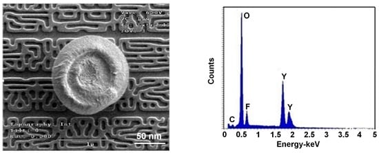
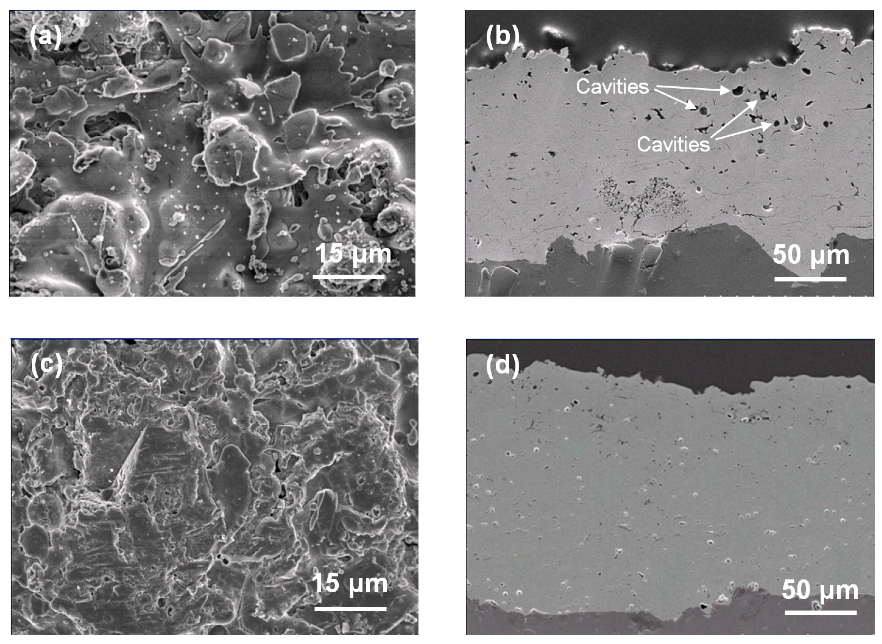
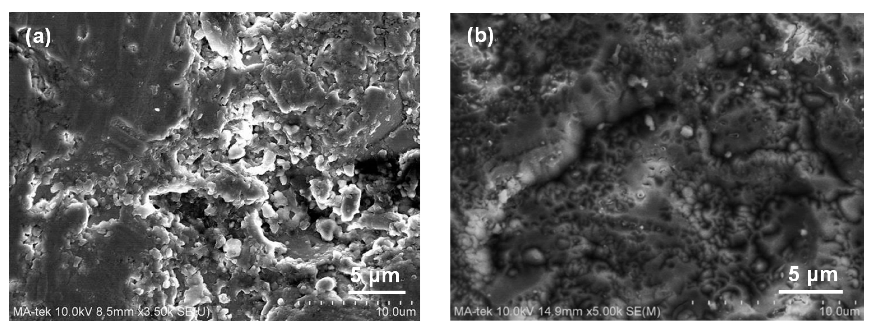
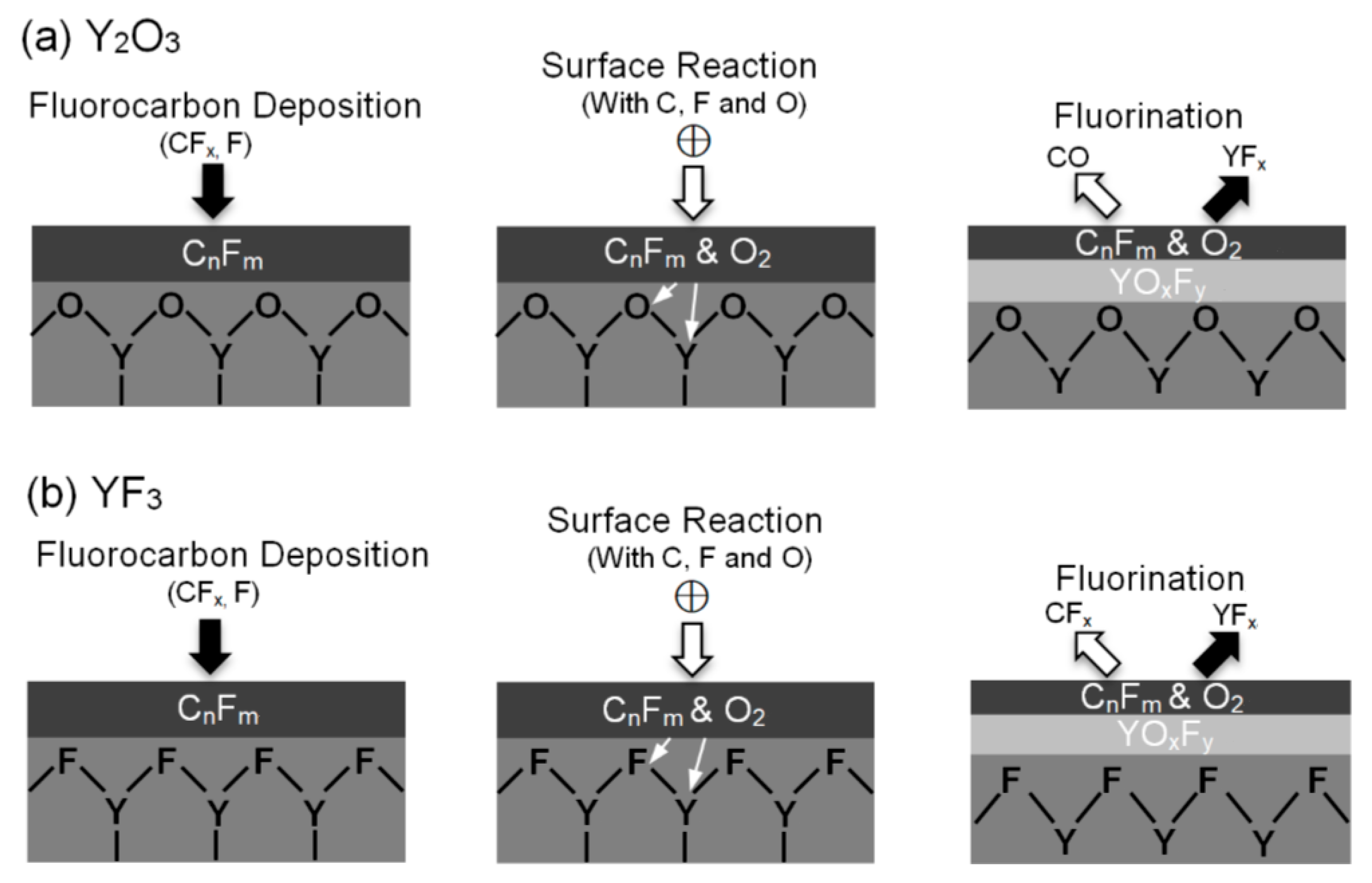
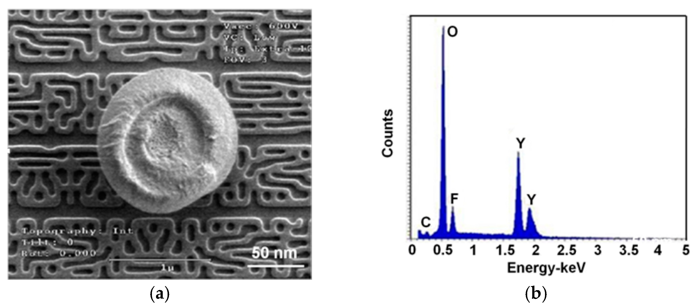
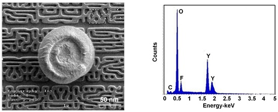
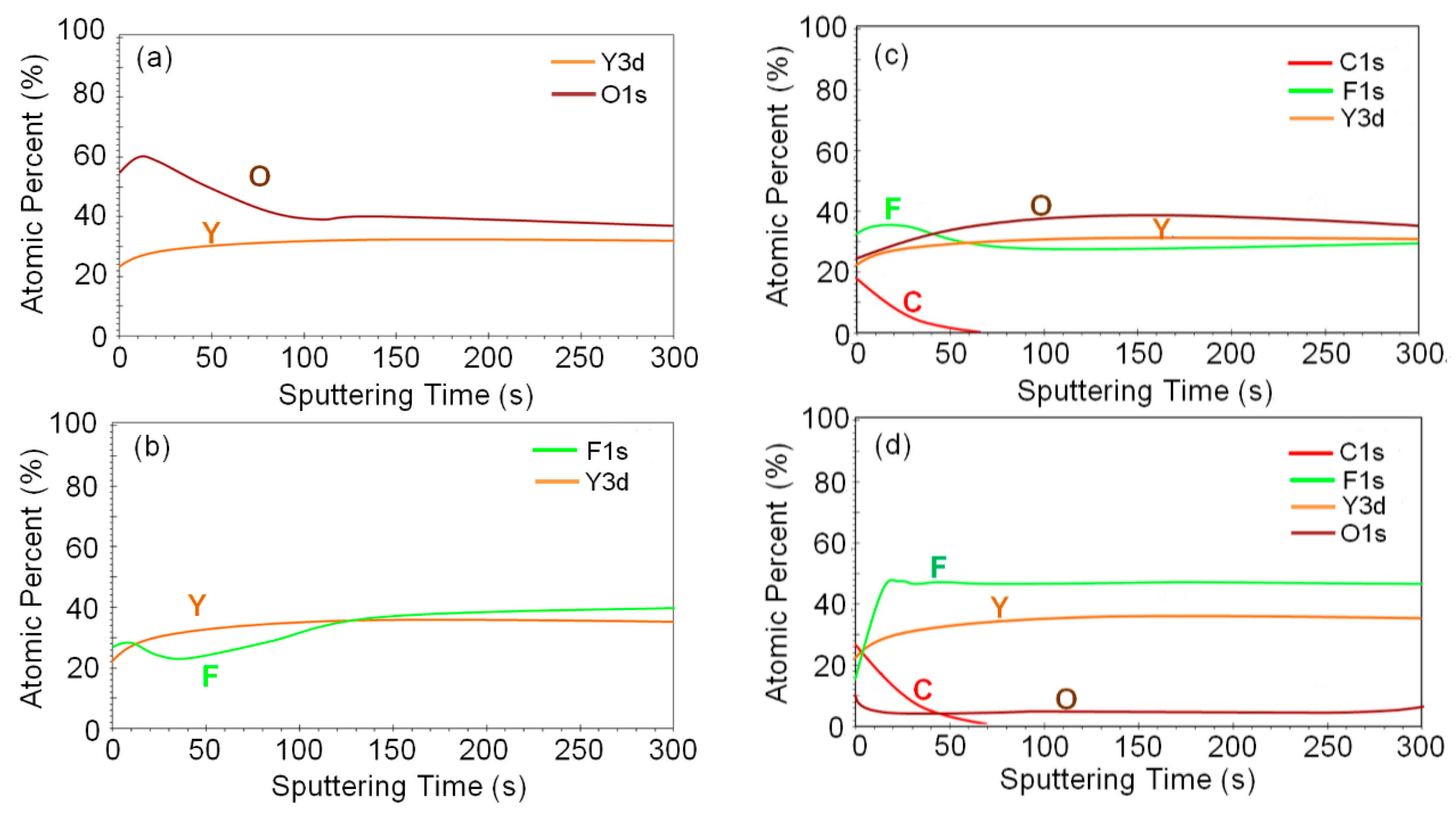
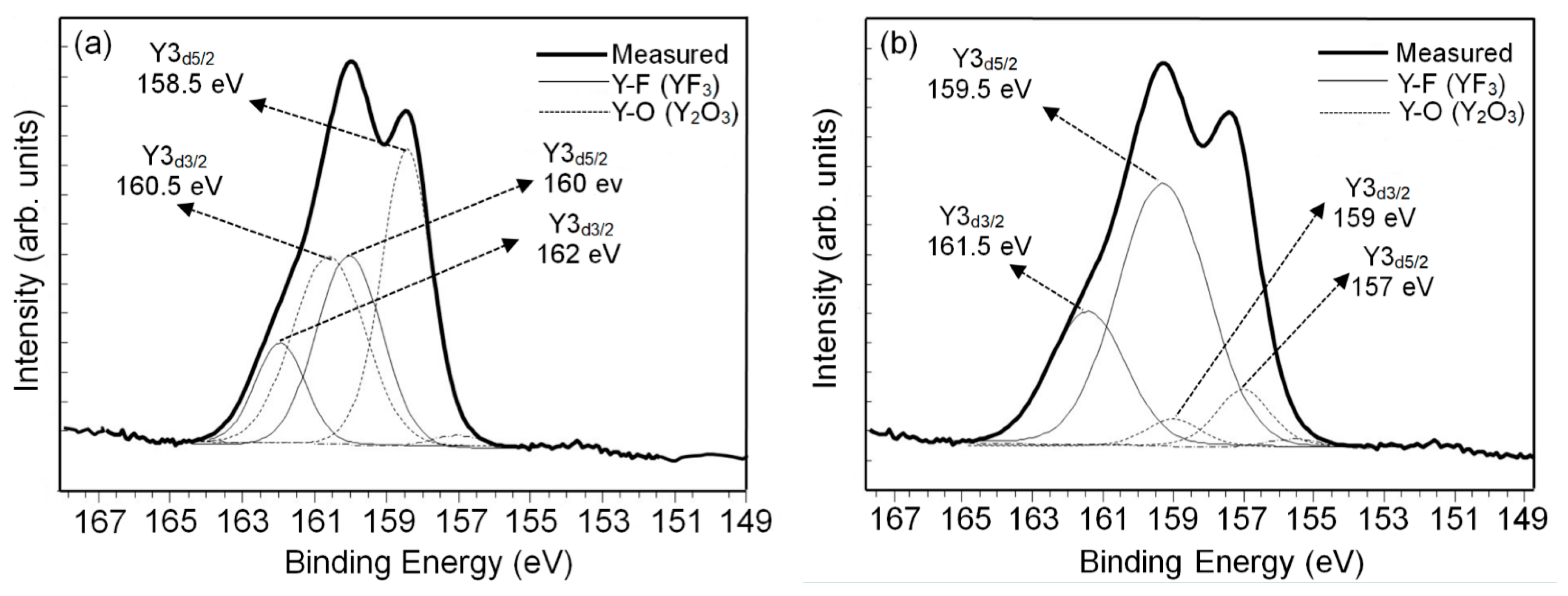
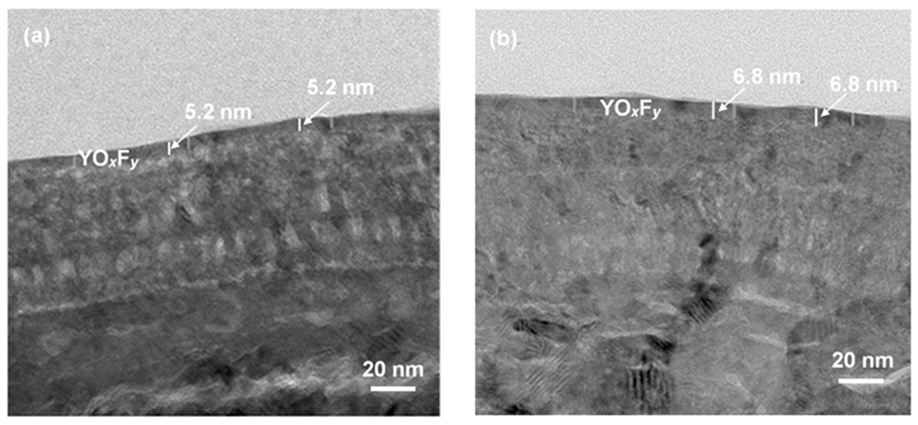
3. Results and Discussion

Figure 2 shows the surface and cross-sectional SEM images of Y2O3 and YF3 coatings under 15 kW plasma spraying powers. Figure 2a shows the Y2O3 coating with poor surface roughness with laminar morphology. A horizontal crack and large cavities (within the size range of 5–10 μm) are also observed (Figure 2b). Dense YF3 coating layers with less porosity are shown in Figure 2c,d). Due to the small difference in thermal expansion between the YF3 coating (28.5 × 10⁻⁶/K) and the Al substrate (23 × 10−6/K), no cracks were observed in any YF3 coating samples. The erosion-resistance characteristics of Y2O3 and YF3 coatings were measured after exposure to the CF4/O2 plasma, as discussed below. Figure 3a,b show the SEM image surface microstructure of the Y2O3 and YF3 coatings after etching in CF4/O2 plasma for 60 min under a bias power of 500 W. There is a large difference in etched surface for both coating samples under the same etching condition. In Figure 3a, the surface of Y2O3 coating is obviously cracked after the etching process. These Y2O3 creaked pieces might be a particle contamination source during the wafer fabrication process. In Figure 3b, the YF3 coating is revealed to have a relatively dense and smooth surface, indicating that the erosion of Y2O3 coating was more severe than YF3 coating after exposure to CF4/O2 plasma. It is also consistent with our previous study regarding the film porosity [16], since the erosion resistance to CF4/O2 plasma (chemical reaction) was enhanced by reducing film porosity [17]. From the SEM observation results, the YF3 coating revealed that a clean and complete surface can be obtained by preventing the fluoride particles from attaching to the etching chamber sidewall after exposure to the fluorocarbon plasma during etching. Hence, the YF3 coating is more favorable for application in plasma processing equipment. Similar results were consistent with the previously reported data by Kim et al. [18].
Figure 4 shows the compositional variation with the sputtering time from the Y2O3 and YF3 coating surfaces after exposure to the CF4/O2 plasma by using XPS. The Y2O3 and YF3 coating surfaces before exposure to the CF4/O2 plasma are shown in Figure 4a,b. The carbon content found on the surface decreased abruptly with the sputtering time, indicating that the carbon polymer layer is very thin (Figure 4c,d). This thin carbon polymer layer on the etched surface was previously reported in Si-based oxide materials etched under fluorocarbon plasma [19,20,21]. Moreover, the fluorine was verified on both Y2O3 and YF3 coatings and the higher fluorine content was detected on the YF3 surface (Figure 4c,d). It was found that the percentage of F atoms reached the maximum value of 35% and 48% on the Y2O3 and YF3 coatings after etching, causing a thicker fluorination layer to appear in the YF3 specimen. This is because YF3 is a fluorine-rich compound material; hence, the chemical composition of F atoms in the YF3 coating was unchanged accompanied with the depth from the surface. The stronger YF3 coating fluorination can also be confirmed by the XPS spectral analysis on etched sample surfaces.
Figure 5 represents the XPS spectra for the yttrium atoms from the (a) Y2O3 and (b) YF3 coating samples after CF4/O2 plasma etching. In the curve-fitted XPS spectra of the Y2O3 coating, two peaks mean two sources of bonding for cations from Y3d split into two Y3d5/2 states (high peaks) and Y3d3/2 (low peaks) [22]. In Figure 5a, the etched surface of the Y2O3 coating consisted of Y3d5/2 and Y3d3/2, with an intensity ratio of 3:2 and peak shift difference in the binding energy of 2 eV, according to the XPS standard [23,24]. This peak shifting to higher binding energy (located at 160 and 162 eV) could be attributed to Y–F bonding in the Y2O3 sample. The higher electronegativity of fluorine (4.0) compared to that of oxygen (3.5) causes higher electron binding energy from the cation [25]. This high fluorine concertation demonstrated that the Y2O transformed into a YOxFy (x + y = 1.5) and/or YFx (x < 3) surface by the exposed fluorine-based plasma [26]. Meanwhile, the two binding energy peaks located at 158.5 and 160.5 eV correspond to a Y–O bond, resulting in a low binding energy. Figure 5b shows the YF3 coating XPS spectra on the etched surface deconvoluted into four peaks, corresponding to Y–F bonding (located at 159.5 and 161.5 eV) and Y–O bonding (located at 157 and 159 eV) [27,28]. Furthermore, the intensity ratio of Y–F to Y–O peaks on the YF3 coating reached 2.9, which was much higher than that of the Y–F to Y–O peak on the Y2O3 coating (0.73), indicating stronger fluorination on the etched YF3 coating surface. These results indicate that the YF3 coating exhibited superior inherent chemical stability after fluorocarbon plasma treatment [29]. The reactions for CF4/O2 plasma chemical etching of Y2O3 and YF3 coatings can be expressed as follows:
Y2O3 + 3CF2* → 2YF3 + 3CO;
YF3 + 2CF2* → YF + 2CF3.
when the CF4/O2 plasma chemical reaction dominates the etching process, and the chemical stability YF3 might be effective in the suppression of particle generation during the etching process, as mentioned in the SEM results.
The microstructures of both coated samples irradiated by high-density CF4/O2 plasma were revealed by TEM. Figure 6a,b shows cross-sectional TEM micrographs of the plasma-etched Y2O3 and YF3 coatings, respectively. A yttrium oxyfluoride (YOxFy) film 5.2 nm in thickness was observed on the Y2O3 surface, while the YF3 sample showed a thicker YOxFy of 6.8 nm. The slightly lesser fluorination of Y2O3 than YF3 is explained by comparing the bonding energies of Y–O (685 KJ/mol) and Y–F (605 KJ/mol). Because the bonding energy of Y–O is higher than Y–F, it results in less-efficient reactions between the Y–O bonding and the fluorocarbon film. The formation of an oxyfluoride layer on the surface of Y2O3 and YF3 coatings might act as a protecting layer to prevent the coating’s surface from further erosion by CF4/O2 plasma.
Figure 7 illustrates the schematic formation mechanism of YOxFy on Y2O3 and YF3 surfaces. The procedure of YOxFy formation on the Y2O3 and YF3 surfaces is as follows: the first step is deposition of the fluorocarbon film by the adsorption of CFx radicals on these two coatings’ sample surfaces. The second step is carbon reactions with oxygen (Y–O) and fluorine (Y–F) to form volatile CO and CFx, resulting in the decomposition of the Y–O and Y–F bondings. Subsequently, the YOxFy film is formed in the Y2O3 and YF3 coatings surface (third step), whereas a part of YFx may desorb from the coating surface. Similar reactions and formation of YOxFy were also investigated previously [30,31]. It is believed that the YOxFy layer is effective in reducing practical generation and thus contamination of the integrated circuit [32].
One of the prime concerns of production yields is the particles generated from the plasma processing equipment, resulting in open- or short-circuits. We have investigated the possible particles generated during the etching process using an in-situ particle monitoring system which can detect the particle trajectories. Figure 8a shows an SEM image of a typical particle observed on the wafer surface. The circular particle is composed of etchant gases and a Y2O3-coated chamber wall after exposed to CF4/O2 plasma—it can be called a partial etch defect. An EDX analysis was carried out to clarify the particle compositions. As shown in Figure 8b, it was found that the flaking particles were composed mainly of yttrium, oxide, and fluoride elements, indicating the particle source from the Y2O3 coating. Therefore, the YF3 coating can behave as a new plasma-facing material that produces fewer contamination particles.

4. Conclusions

During the plasma etching process, particles generated from the Y2O3 and YF3 protective coatings of the ICP chamber wall were investigated in this study. The particle generation mechanism could be due to the fact that the bonding strength of Y–O was weaker than that of Y–F when the chamber-wall surface suffered irradiation from high-density CF4/O2 plasmas. From the SEM examination results, YF3 was also confirmed to be more robust than Y2O3 against CF4/O2 plasma irradiation. The YF3 coatings for the ICP etching chamber components and materials can play an important role in decreasing the extreme number of particles in the fluorine-based plasma environment.

Acknowledgments

This work was supported by the Ministry of Science and Technology (Taiwan) with Grant Nos. 105-2622-8-005-003-TE1 and 105-2221-E-005-059-MY3. The authors wish to express their sincere gratitude for the financial and technical support from the advanced Industry Technology Centre of National Chung Hsing University, Taiwan.

Author Contributions

Tzu-Ken Lin and Dong-Sing Wuu proposed the concept. Tzu-Ken Lin and Wei-Kai Wang conceived and designed the experiments. Tzu-Ken Lin, Shih-Yung Huang and Chi-Tsung Tasi contributed the films measurement results. Tzu-Ken Lin, Wei-Kai Wang and Dong-Sing Wuu wrote the manuscript. All authors read and approved the final version of the manuscript to be submitted.

Conflicts of Interest

The authors declare no conflict of interest.

References

  1. Zavareh, M.A.; Sarhen, A.A.D.M.; Razak, B.B.; Basirun, W.J. Plasma thermal spray of ceramic oxide coating on carbon steel with enhanced wear and corrosion resistance for oil and gas applications. Ceram. Int. 2014, 40, 14267–14277. [Google Scholar] [CrossRef]
  2. Kim, D.M.; Kim, K.B.; Yoon, S.Y.; Oh, S.Y.; Kim, H.T.; Lee, S.M. Effects of artificial pores and purity on the erosion behaviors of polycrystalline Al2O3 ceramics under fluorine plasma. J. Ceram. Soc. 2009, 117, 863–867. [Google Scholar] [CrossRef]
  3. Cardinaud, C.; Peignon, M.C.; Tessier, P.Y. Plasma etching: principles, mechanisms, application to micro- and nano-technologies. Appl. Surf. Sci. 2000, 164, 72–83. [Google Scholar] [CrossRef]
  4. Cunge, G.; Inglebert, L.; Joubert, O.; Vallier, L.; Sadeghi, N. Ion flux composition in HBr Cl2/O2 and HBr/Cl2/O2/CF4 chemistries during silicon etching in industrial high-density plasmas. J. Vac. Sci. Technol. 2002, 20, 2137–2148. [Google Scholar] [CrossRef]
  5. Fukumoto, H.; Fujikake, I.; Takao, Y.; Eriguchi, K.; Ono, K. Plasma chemical behavior of reactants and reaction products during inductively coupled CF4 plasma etching of SiO2. Plasma Sources Sci. Technol. 2009, 18, 045027. [Google Scholar] [CrossRef]
  6. Ito, N.; Moriya, T.; Uesugi, F.; Matsumoto, M.; Liu, S.; Kitayama, Y. Reduction of particle contamination in plasma-etching equipment by dehydration of chamber wall. Jpn. J. Appl. Phys. 2008, 47, 3630–3634. [Google Scholar] [CrossRef]
  7. Sato, N.; Uchida, G.; Kaneko, T.; Shimizu, S.; Iizuka, S. Dynamics of fine particles in magnetized plasmas. Phys. Plasmas 2001, 8, 1786–1790. [Google Scholar] [CrossRef]
  8. Kim, D.M.; Lee, S.H.; Alexander, W.B.; Kim, K.B.; Oh, Y.S.; Lee, S.M. X-Ray photoelectron spectroscopy study on the interaction of yttrium–aluminum oxide with fluorine-based plasma. J. Am. Ceram. Soc. 2011, 94, 3455–3459. [Google Scholar] [CrossRef]
  9. Qin, X.P.; Zhou, G.H.; Yang, H.; It Wong, J.; Zhang, J.; Luo, D.W.; Wang, S.W.; Ma, J.; Tang, D.Y. Fabrication and plasma resistance properties of transparent YAG ceramics. Ceram. Int. 2012, 38, 2529–2535. [Google Scholar] [CrossRef]
  10. Iwasawa, J.; Nishimizu, R.; Tokita, M.; Kiyohara, M. Plasma-resistant dense yttrium oxide film prepared by aerosol deposition process. J. Am. Ceram. Soc. 2007, 90, 2327–2332. [Google Scholar] [CrossRef]
  11. Mun, S.Y.; Shin, K.C.; Lee, S.S.; Kwak, J.S.; Jeong, J.Y.; Jeong, Y.H. Etch defect reduction using SF6/O2 plasma cleaning and optimizing etching recipe in photo resist masked gate poly silicon etch process. Jpn. J. Appl. Phys. 2005, 44, 4891–4894. [Google Scholar] [CrossRef]
  12. Ramos, R.; Gunge, G.; Joubert, O.; Sadeghi, N.; Mori, M.; Vallier, L. Plasma/react walls interactions in advanced gate etching process. Thin Solid Films. 2007, 515, 4846–4852. [Google Scholar] [CrossRef]
  13. Rueger, N.R.; Beulens, J.J.; Schaepkens, M.; Doemling, M.F.; Mirza, J.M.; Standaert, T.E.F.M.; Oehrlein, G.S. Role of steady state fluorocarbon films in the etching of silicon dioxide using CHF3 in an inductively coupled plasma reactor. J. Vac. Sci. Technol. 1997, 15, 1881–1889. [Google Scholar] [CrossRef]
  14. Standaert, T.E.F.M.; Hedlund, C.; Joseph, E.A.; Oehrlein, G.S.; Dalton, T.J. Role of fluorocarbon film formation in the etching of silicon, silicon dioxide, silicon nitride, and amorphous hydrogenated silicon carbide. J. Vac. Sci. Technol. 2004, 22, 53–60. [Google Scholar] [CrossRef]
  15. Schaepkens, M.; Standaert, T.E.F.M.; Rueger, N.R.; Sebel, P.G.M.; Cook, J.M. Study of the SiO2-to-Si3N4 etch selectivity mechanism in inductively coupled fluorocarbon plasmas and a comparison with the SiO2-to-Si mechanism. J. Vac. Sci. Technol. 1999, 17, 26–37. [Google Scholar] [CrossRef]
  16. Lin, T.K.; Wuu, D.S.; Huang, S.Y.; Wang, W.K. Characteristics of yttrium fluoride and yttrium oxide coatings for plasma process equipment prepared by atmospheric plasma spraying. Jpn. J. Appl. 2016, 55, 162601. [Google Scholar] [CrossRef]
  17. Cao, Y.C.; Zhao, L.; Luo, J.; Wang, K.; Zhang, B.P.; Yotoka, H.; Ito, Y.; Li, J.F. Plasma etching behavior of Y2O3 ceramics: Comparative study with Al2O3. App. Surf. Sci. 2016, 336, 304–309. [Google Scholar] [CrossRef]
  18. Kim, D.M.; Oh, Y.S.; Kim, S.; Kim, H.T.; Lim, D.S.; Lee, S.M. The erosion behaviors of Y2O3 and YF3 coatings under fluorocarbon plasma. Thin Solid Films 2011, 519, 6698–6702. [Google Scholar] [CrossRef]
  19. Standaert, T.E.F.M.; Schaepkens, M.; Rueger, N.R.; Sebel, P.G.M.; Oehrlein, G.S.; Cook, J.M. High density fluorocarbon etching of silicon in an inductively coupled plasma: Mechanism of etching through a thick steady state fluorocarbon layer. J. Vac. Sci. Technol. 1998, 16, 239–249. [Google Scholar] [CrossRef]
  20. Tatsumi, T.; Matsui, M.; Okigawa, M.; Sekine, M. Control of surface reactions in high-performance SiO2 etching. J. Vac. Sci. Technol. 2000, 18, 1897–1902. [Google Scholar] [CrossRef]
  21. Matsui, M.; Tatsumi, T.; Sekine, M. Observation of surface reaction layers formed in highly selective SiO2 etching. J. Vac. Sci. Technol. 2001, 19, 1282–1888. [Google Scholar] [CrossRef]
  22. Korzenski, M.B.; Lecoeur, P.; Mercey, B.; Chippaux, D.; Raveau, B. PLD-grown Y2O3 thin films from Y metal: An advantageous alternative to films deposited from yttria. Chem. Mater. 2000, 12, 3139–3150. [Google Scholar] [CrossRef]
  23. Moulder, J.F.; Stickle, W.F.; Sobol, P.E.; Bomben, K.D. Handbook of X-ray Photoelectron Spectroscopy; Physical Electronics: Eden Prairie, MN, USA, 1995; p. 10. [Google Scholar]
  24. Pei, L.; Jiapi, Z.; Yuankun, Z.; Jiecai, H. Preparation and optical properties of sputtered-deposition yttrium fluoride film. Nucl. Instrum. Methods Phys. Res. 2013, 307, 429–433. [Google Scholar] [CrossRef]
  25. Vickerman, J.C.; Gilmore, I.S. Surface Analysis, 2nd ed.; Wiley: New York, NY, USA, 2009; p. 53. [Google Scholar]
  26. Cunge, G.; Pelissier, B.; Joubert, O.; Ramos, R.; Maurice, C. New chamber walls conditioning and cleaning strategies to improve the stability of plasma processes. Plasma Sources Sci. Technol. 2005, 14, 599–609. [Google Scholar] [CrossRef]
  27. Zhong, H.X.; Hong, J.M.; Cao, X.F.; Chen, X.T.; Xue, Z.L. Ionic-liquid-assisted synthesis of YF3 with different crystalline phases and morphologies. Mater. Res. Bull. 2009, 44, 623–628. [Google Scholar] [CrossRef]
  28. Barve, S.A.; Jagannath; Mithal, N.; Deo, M.N.; Chand, N.; Bhanage, B.M.; Gantayet, L.M.; Patil, D.S. Microwave ECR plasma CVD of cubic Y2O3 coatings and their characterization. Surf. Coat. Technol. 2010, 204, 3167–3172. [Google Scholar] [CrossRef]
  29. Kim, D.M.; Jang, M.R.; Oh, Y.S.; Kim, S.; Lee, S.M.; Lee, S.H. Relative sputtering rates of oxides and fluorides of aluminum and yttrium. Surf. Coat. Technol. 2017, 309, 694–697. [Google Scholar] [CrossRef]
  30. Levin, I.; Huang, Q.Z.; Lawrence, P.C.; Winnie, W.N. Non-quenchable chemical order-disorder phase transition in yttrium oxyfluoride YOF. Eur. J. Inorg. Chem. 2005, 1, 87–91. [Google Scholar] [CrossRef]
  31. Miwa, K.; Takada, N.; Sasaki, K. Fluorination mechanisms of Al2O3 and Y2O3 surfaces irradiated by high-density CF4/O2 and SF6/O2 plasmas. J. Vac. Sci. Technol. 2009, 27, 831–835. [Google Scholar] [CrossRef]
  32. Tsunoura, T.; Yoshida, K.; Yano, T.; Kishi, Y. Fabrication, characterization, and fluorine-plasma exposure behavior of dense yttrium oxyfluoride ceramics. Jpn. J. Appl. 2017, 56, 06HC02. [Google Scholar]
Figure 1. Schematic illustration of the cross section of inductively coupled plasma (ICP) etching tool.
Nanomaterials 07 00183 g001
Figure 2. Surface and cross-sectional SEM images of (a,b) Y2O3 and (c,d) YF3 coating at plasma spray power of 15 kW.
Nanomaterials 07 00183 g002
Figure 3. SEM images after fluorocarbon plasma treatment: (a) Y2O3 and (b) YF3 coatings.
Nanomaterials 07 00183 g003
Figure 4. Variations of chemical compositions measured using X-ray photoelectron spectroscopy (XPS) with the sputtering time of (a,c) the Y2O3 and (b,d) the YF3 coatings before and after exposure to the fluorocarbon plasma.
Nanomaterials 07 00183 g004
Figure 5. Variations of chemical compositions measured using XPS with the sputtering time of (a) the Y2O3 and (b) the YF3 coatings after exposure to the fluorocarbon plasma.
Nanomaterials 07 00183 g005
Figure 6. TEM microstructures of (a) Y2O3 and (b) YF3 coatings after exposure to the fluorocarbon plasma.
Nanomaterials 07 00183 g006
Figure 7. Schematic illustration of yttrium oxyfluoride film deposition behavior on (a) Y2O3 and (b) YF3 coatings.
Nanomaterials 07 00183 g007
Figure 8. (a) SEM image of a circular particle and (b) energy dispersive X-ray diffraction (EDX) analysis results of circular particle.
Nanomaterials 07 00183 g008
Table 1. Spraying parameters for coatings made of Y2O3 and YF3.
ConditionY2O3YF3
Primary gas flow rate (L/min)4545
Secondary current (L/min)66
Gun moving rate (cm/s)1010
System voltage (V)5050
Gun power (kW)1515
Stand-off (cm)1010
Table 2. Plasma etching parameters for Y2O3 and YF3 coatings.
ConditionY2O3YF3
RF source power (W)13001300
RF bias power (W)500500
Chamber pressure (Pa)1.061.06
CF4:O2 (sccm)30:530:5
Etching time (min)6060

