Defect-Induced Tunable Permittivity of Epsilon-Near-Zero in Indium Tin Oxide Thin Films


1
Engineering Research Center of Optical Instrument and System, Ministry of Education and Shanghai Key Lab of Modern Optical System, University of Shanghai for Science and Technology, Shanghai 200093, China
2
School of Electrical and Electronic Engineering, Nanyang Technological University, Singapore 639798, Singapore
*
Author to whom correspondence should be addressed.
Nanomaterials 2018, 8(11), 922; https://doi.org/10.3390/nano8110922
Submission received: 18 October 2018
/
Revised: 2 November 2018
/
Accepted: 5 November 2018
/
Published: 7 November 2018
(This article belongs to the Special Issue Dielectric Nanophotonics and Their Applications)
Abstract
:Defect-induced tunable permittivity of Epsilon-Near-Zero (ENZ) in indium tin oxide (ITO) thin films via annealing at different temperatures with mixed gases (98% Ar, 2% O2) was reported. Red-shift of λENZ (Epsilon-Near-Zero wavelength) from 1422 nm to 1995 nm in wavelength was observed. The modulation of permittivity is dominated by the transformation of plasma oscillation frequency and carrier concentration depending on Drude model, which was produced by the formation of structural defects and the reduction of oxygen vacancy defects during annealing. The evolution of defects can be inferred by means of X-ray diffraction (XRD), atomic force microscopy (AFM), and Raman spectroscopy. The optical bandgaps (Eg) were investigated to explain the existence of defect states. And the formation of structure defects and the electric field enhancement were further verified by finite-difference time domain (FDTD) simulation.
1. Introduction
Searching for better plasmonic materials was of great significance for the application of various ultrasensitive plasmonic devices [1,2,3,4]. However, most of the current plasmonic materials like noble metals exhibit limited tunability and feature high extinction losses in the range of visible and NIR spectra [5,6,7,8,9,10]. In recent years, transparent conductive oxides (TCOs) have been chosen as alternative plasmonic materials that include ITO, Al- or Ga-doped Zn oxides (AZO/GZO), and a mixed family of these oxides [11]. As a result of the absence of interband transitions, the imaginary part of dielectric constant of TCOs is smaller than that of noble metal [12]. Since TCOs can be heavily doped, their carrier concentration will be accordingly changed to tune the optical properties of them [13]. Furthermore, the dielectric constant of TCOs can be flexibly tuned and the Epsilon-Near-Zero (ENZ) behavior has been achieved in a wide range of spectrum [14,15,16]. According to the above, plasmonic TCOs (especially ITO) have been widely used in plasmonics, nonlinear optics, and metamaterials, such as perfect absorption [17,18,19], electro-optical modulation [20,21,22], switching [23,24,25], beam steering [26], nonlinear generation enhancement [14,15], and negative refraction [27,28,29].
A number of studies have mirrored that post-annealing treatment can tune the structural properties of ITO thin films which were deposited on different substrates [30,31,32], by controlling the gaseous atmospheres [33,34] or annealing temperature [35,36,37]. The electrical properties like free-carrier concentration have also been modulated combined with the change of the optical properties even the ENZ characteristics [38,39,40]. When it comes to the internal carrier transport of ITO films, many scattering mechanism were researched such as oxygen vacancy. In vacancy, doping of tin atom can cause ionized impurities, grain barriers, dislocation defect, and crystallographic defects [41,42,43,44]. What is more, other researchers adopted a post-annealing procedure to modify optical-electrical properties [45,46]. There are a few of reports concerning ENZ characteristics in NIR spectral ranges of ITO thin films which grow on K9 glass substrates by electron beam (EB) evaporation method.
In this work, a tunable permittivity of ENZ in indium tin oxide (ITO) thin films was realized via annealing. The surface morphology and crystallinity of samples were investigated at the beginning. Then, in order to characterize the dielectric and spectral properties of the films, we measured the permittivity and absorption spectra. To describe the mechanism of tunable permittivity, the Drude model was introduced. Meanwhile, the plasma frequency, carrier relaxation time, and optical bandgaps were theoretically and experimentally researched to explain the changes of optical properties [47,48,49]. Furthermore, the oxygen vacancy defect states and vibrational levels within ITO films were analyzed by Raman scattering spectra. At last, we verify the enhancement of absorption and the evolution of internal defects in the films by FDTD (finite-difference time domain) solutions.
2. Materials and Methods
Before deposition, the K9 glass substrates were ultrasonically cleaned in acetone, ethanol, and deionized water for 20 min, respectively, and then dried with a nitrogen flow. ITO thin films were grown by electron beam (EB) evaporation from ITO coating materials (90 wt.% In2O3 and 10 wt.% SnO2 target, 99.99% purity) with baking temperature set at 370 °C and a base pressure less than 5 × 10⁻⁴ Pa. The target thicknesses of 80 nm were monitored by a quartz crystal microbalance. All substrates were place on the fixture with the same radius away from the axis to ensure the uniformity of the film thickness.
Postdeposition annealing treatments had been carried out using a high temperature tubular furnace (SG-GL 1200K, Shanghai, China). All the ITO films annealing in mixed gases (98% Ar, 2% O2) were maintained for 60 min at three target temperatures of 150 °C, 300 °C, and 450 °C before a 5 °C per minute heating rate performed during the procedure under normal pressure. For comparison, an as-deposited film on bare substrate was grown in our work. As-deposited film and as-annealed films were indicated as S0, S1 (150 °C), S2 (300 °C), and S3 (450 °C) respectively.
The structural properties and the crystallinity of the films were measured by a Bruker AXS/D8 Advance X-ray diffraction (XRD) system (Bruker, Billerica, MA, USA) with Cu kα radiation (λ = 0.15408 nm). The surface morphology and roughness were characterized by AFM (atomic force microscopy) (XE-100, Park System, Suwon, Korea). The optical absorption was measured with an UV-Vis-NIR double beam spectrophotometer (Lambda 1050, Perkins Elmer, Waltham, MA, USA). The sheet resistances of films were measured by four-point probe resistivity measurement system. Hall measurements (HMS-3000, ECOPIA, Anyang, Korea) were conducted to determine the electron mobility, sheet resistance, resistivity, and free carrier concentration of the films. The dielectric constant characteristics were taken from spectroscopic ellipsometry (UVISEL-ER, HORIBA, Oberursel, Germany). The Raman spectrum was carried out by a confocal microprobe Raman system (inVia Raman Microscope, Renishaw, Pliezhausen, Germany) with a 633 nm operation wavelength. The analysis of the data used the finite-difference time domain (FDTD).
3. Results and Discussion
3.1. Microstructural Properties and Surface Morphology
Figure 1a shows the XRD patterns which reveal the crystallinity of the samples. All the ITO films present the preferential orientation at approximately 30.58° (2θ) which corresponds to the (222) crystallographic plane of ITO according to the standard card of ITO (JCPDS: 06-0416). Other peaks appear at 2θ = 35.47° (400), 2θ = 51.04° (440), and 2θ = 60.68° (622). It is known that the growth orientation is biased towards the lowest surface energy. During the annealing procedure, the In charge is melted with the broken portion of the crystallographic texture. Parts of the atoms and so-called defects were evaporated and the others migrate through the substrate from the upper surface state to the lower due to the lowest principle of energy [50]. At the same time, all of these defects or atoms will annihilate and agglomerate within the internal structure resulting in recrystallization. This process constantly occurs in the structural transformation of ITO at the temperature range. However, the grain size is increased slightly during the annealing process. The recrystallization procedure can be deduced from both XRD (Figure 1b) and AFM results (Figure 2).
The average grain size is calculated by Scherrer formula, using FWHM (full-width at half-maximum) values of the XRD diffraction peaks as follows [51] where D is the grain size, λ (=1.5406 Å) is the wavelength of X-ray radiation, θ the diffraction angle, and β is the FWHM which is obtained from MDI Jade analysis. The average grain sizes of S0, S1, S2, and S3 are 39.391, 39.764, 42.43, and 49.286 nm, respectively (Table 1). We can also see that the d-value (interplanar spacing) of the films exhibit a difference due to the change of residual stress. The diffraction peaks are 30.320°, 30.360°, 30.341°, and 30.417° (2θ), respectively. The FWHM values of S0, S1, S2, and S3 are 0.209°, 0.207°, 0.194°, and 0.167°, respectively. Figure 1b points out that the average grain size and the FWHM are related to the annealing temperature in (222) crystallographic plane. With the temperature increasing, the grain size is increased slightly. The FWHM of the as-annealed samples was narrow than that of the as-deposited sample. The results consist of the broken of the crystallographic texture and the agglomeration of the grain (as shown in Figure 2a–d).
Figure 2 reveals the AFM images and the root-mean-square surface roughness (RMS) of samples as a function of annealing temperatures with the scanning area of 2 × 2 μm. Obviously, the surface morphology of as-deposited film is uniform and well-distributed so that the value of RMS is relatively small. When annealing at 150 °C, the film turns into valley-like and crisscross along with a large grain size consisted with Figure 1. When the temperature increases to 300 °C or 450 °C, the surface transforms from smooth to ups and downs. Owing to the local thermal effect and the increased heat transferring from furnace to the films, the interior recombination of intrinsic atoms and defects occurs leading to grain growth. This is also consistent with the XRD results which show a better crystalline of the samples after annealing. What is more, the measured RMS values consist with the surface patterns in Figure 2. All these changes were attributed to the increased grain size and induced defects [35].
3.2. Optical Constants
3.2.1. Optical Permittivity
The optical permittivity ε(ω) of ITO films was investigated by spectroscopic ellipsometry method. Figure 3 expresses the measured permittivity which illustrates the influence of the annealing procedure on the real (ε) and imaginary (ε) parts of ε(ω). From Figure 3 and the inset figure, ITO films show an ENZ condition which is denoted by λENZ [52,53]. The λENZ of ITO films are 1422 nm (S0), 1504 nm (S1), 1730 nm (S2), and 1995 nm (S3), respectively. Accordingly, when the ENZ wavelength (λENZ) shifts to red and the imaginary permittivity reduces to less than 1 with increasing temperature. Furthermore, the real permittivity is nearly zero while the imaginary part is smaller than 1 which guarantees the internal fields enhancement that supports the ENZ condition in ITO films.
The Drude–Sommerfeld model is adequately introduced to describe the mechanism of the optical constants of ITO film [13,49]:
Here, ε∞ is the high frequency limit of εITO, ωp is the plasma frequency, and Γ expresses the charge carrier collision rate, which leads to the optical losses ε2 inside the film. The plasma frequency can be described as
where n is the carrier concentration, ε0 is the permittivity of free space, e is electron charge, and m* is the effective mass of electron, respectively. Generally, for the sake of negative permittivity, a large free carrier concentration with the order of 1020 to 1022 cm−3 is needed. The intrinsic doping is so large in ITO film that brings about the ENZ characteristic in the NIR region. Therefore, ITO films exhibit metal behavior in the NIR range [10,13]. We can learn from Equations (1) and (2) that the plasma frequency, charge carrier collision rate, and carrier concentration may alter the optical permittivity of the films. It will be discussed in the following sections.
3.2.2. Optical Bandgap and Optical Absorption
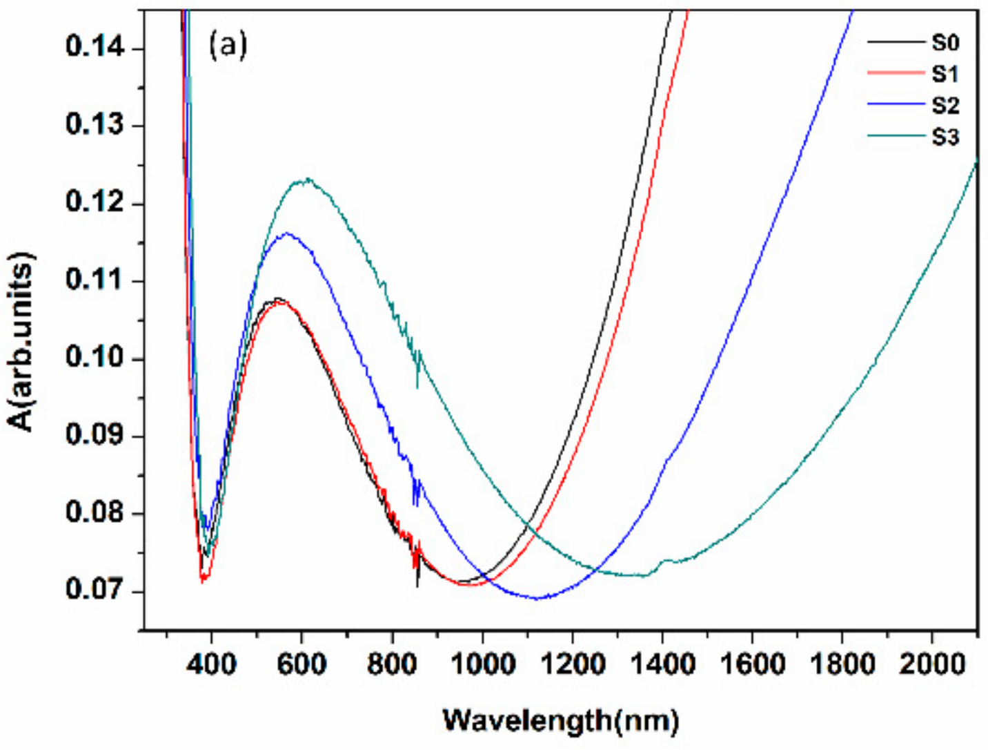
Here, the optical absorption was measured first to check the effects of structure defects. Meanwhile, the optical bandgap shift was experimentally calculated using Tauc’s method to learn the relationship between the oxygen vacancies and the bandgap properties of ITO films [47,48]. As shown in Figure 4a, the absorption in visible enhances and redshifts but dropped off in NIR. It can be interpreted as the light trapping effect promoted by the rough structure defects [54,55]. Figure 4b shows that the bandgap narrows after annealing. It can be inferred that the defect energy levels generated by structure and oxygen vacancy defects act as the intermediate level. When the photon energy is applied to the films, electron transitions were taken place from valence band to defect energy level and then to the conduction band [42,56,57]. Consequently, lower energy is needed during the transition progress consistent with the red shift of absorption and the narrowing of bandgap.
Theoretically, it is clear that
where A is optical absorbance, α is absorption coefficient, T is optical transmittance, R is the total reflectance coefficient, and d represents the film thickness. The optical bandgap Eg for a direct-gap semiconductor can be described by a function of frequency ω:
According to Burstein–Moss shift effect, the bandgap Eg has a connection with carrier concentration n, which is described as [58]
Here, Eg0 is the intrinsic bandgap, n is the carrier concentration, and m* indicates the effective mass of electron (here m* of ITO is an approximately constant: 0.38m0 [59,60,61]).
Based on the formula above, while the annealing temperature rises, the bandgap Eg decreases due to the diminution of carrier concentration n. From Figure 4a it can be see that the optical absorption shows a red shift from 546 nm to 610 nm owing to the electron transition from the valence band to the defect energy levels, or from the defect to the conduction band [62,63,64]. Moreover, Figure 4c suggests the calculated ħωp and extrapolated Eg as a function of annealing temperature. With the increase of temperature, the values are decreasing, but the difference between them is more obvious. We calculate the absorption coefficient by Formula (4), catching an upward tendency which is consistent with Figure 4a. Finally, all of the variation is owing to the internal carrier fundamentally changes which root in the recombination of internal structure.
3.3. Electrical Properties
To explore the electrical mechanism, the bulk carrier concentration n, sheet carrier concentration n’, the electron mobility μ, and resistivity ρ were measured by Hall Effect measurement. Meanwhile, we calculated the plasma frequency ωp, carrier relaxation time τ and sheet resistance Rs’ by Equation (2) combined with the following formula.
All of the electrical relevant data mentioned above are shown in Figure 5a–d.
Figure 5 shows the reduction of the plasma frequency and carrier relaxation time (Figure 5a) due to the decrease of carrier concentration and mobility (Figure 5b) as the annealing temperature rise. During the annealing procedure, the structure defects in ITO films scatter the free carrier resulting in the reduction of mobility. The decrease of sheet/bulk carrier concentration (Figure 5d) is attributed to the oxygen vacancy reduction and the carrier trapping effect in the rough surface structure [41]. The resistivity (Figure 5c) of ITO films tested by the two methods fits well and fits with the evolution of carrier concentration and mobility. What is more, the downtrend of calculated ωp and τ can also be certified by the red-shift of absorption spectra reckoned from Figure 5a–c. Equations (1)–(7) connect the dielectric properties and electrical performance of ITO in this work. These equations imply that It is easy to explain the tunability of the permittivity by the free carrier mechanism that has a key role in determining the plasma frequency ωp. This carrier mechanism is due to the defect modulation discussed earlier; it also infers that .
3.4. Raman Spectra and FDTD Simulation
The oxygen vacancy defect states and stretching vibrational levels within ITO films were researched by Raman scattering. ITO has been proven to have 22 Raman responsive and 16 infrared responsive modes. The 499 cm−1 mode is rooted in the bending and stretching vibrations of InO6 octahedra. The oxygen vacancy defect has a great influence on the vibration of In–O–In bond, and it also causes the change of Raman scattering intensity and the shift of Raman peak position since the scattering intensity is proportional to the square of the derivative of the polarizability [56]. Here, we attribute the change of Raman spectra intensity to the reduction of oxygen vacancies and the rough surface. According to Figure 6, high frequency sets at 499 cm−1 are typically assigned to bcc (body-centered cubic)-In2O3 [65,66,67,68]. The blue-shift and the decreased intensity of 499 cm−1 peak demonstrate that there are fewer oxygen vacancies in ITO films after annealing according [65]. It indicates that oxygen vacancies are partially filled during the annealing procedure [69]. The broken of In–O–In bond also can be confirmed by the dissociated and agglomerated rough structure.
To further verify the absorption changes and the optoelectronic properties of the films, the electric field distribution on the rough surface was simulated by FDTD solutions. During the calculation, a 600-nm (consistent with the optical absorption peak wavelength) laser was irradiated perpendicular to the x-y plane of the ITO film and polarized along the y-axis. The values of different parameters including optical refractive index and RMS applied in the model are consistent with the experiment data. According to Figure 7a, the electric field is well-distributed and the enhancement effect is not significant due to the smooth surface. With the temperature increasing, the electric field intensity enhances and the density of free electrons begins to appear maldistributed. This result is consistent with the reduction of free carrier concentration owing to the increase of internal structure defects and the decrease of oxygen vacancies. The surface “hot spots” (as shown in Figure 7b–d) verify the enhancement of absorption. The defects in the ITO thin film enhanced the localized surface electric field and visible absorption intensity. The simulation results fit well with the experimental evidence.
4. Conclusions
In conclusion, the photoelectric properties of single-layer ITO thin films were modulated by a simple post-annealing method. Red-shift of λENZ (Epsilon-Near-Zero wavelength) from 1422 nm to 1995 nm in wavelength was achieved. XRD and AFM results indicated that structure defects were induced and oxygen vacancies were filled during the annealing procedure that led to the degradation of free carrier concentration and mobility. The reduction of plasma frequency prompted the red shift of absorption with the decreased optical losses. The bandgaps were narrowed with the generation of defect levels. Raman scattering demonstrated the reduction of oxygen vacancies. FDTD solutions further verified the enhanced electric field distribution and optical absorption. It is possible to tailor the characteristics of ITOs through appropriate postdeposition treatment; making widely tunable ENZ ITO films will open up new opportunities in optoelectronic applications.
Author Contributions
Conceptualization, J.L. and D.Z. (Dawei Zhang); Methodology, J.L., R.H., and D.Z. (Daohua Zhang); Software, J.L. and P.Q.; Validation, J.L., D.Z. (Dawei Zhang), R.H., and D.Z. (Daohua Zhang); Formal Analysis, J.L. and T.L.; Investigation, J.L. and R.H.; Resources, J.L. and D.Z. (Dawei Zhang); Data Curation, J.L. and R.H.; Writing—Original Draft Preparation, J.L.; Writing—Review and Editing, J.L., D.Z. (Dawei Zhang), R.H., P.Q., T.L., and D.Z. (Daohua Zhang).
Funding
This work was partially supported by the National Natural Science Foundation of China 61775140 and 61775141, the Shanghai Foundation for Science and Technology Innovation Action Plan 15441902302 and 1714220060, and the National Key Research and Development Program of China 2016YFB1102303.
Conflicts of Interest
The authors declare no conflicts of interest.
References
- Brewer, S.H.; Franzen, S. Optical properties of indium tin oxide and fluorine-doped tin oxide surfaces: Correlation of reflectivity, skin depth, and plasmon frequency with conductivity. J. Alloys Compd. 2002, 338, 73–79. [Google Scholar] [CrossRef]
- Brewer, S.H.; Franzen, S. Calculation of the electronic and optical properties of indium tin oxide by density functional theory. Chem. Phys. 2004, 300, 285–293. [Google Scholar] [CrossRef]
- And, S.H.B.; Franzen, S. Indium Tin Oxide Plasma Frequency Dependence on Sheet Resistance and Surface Adlayers Determined by Reflectance FTIR Spectroscopy. J. Phys. Chem. B 2002, 106, 12986–12992. [Google Scholar]
- Franzen, S. Surface Plasmon Polaritons and Screened Plasma Absorption in Indium Tin Oxide Compared to Silver and Gold. J. Phys. Chem. C 2008, 112, 6027–6032. [Google Scholar] [CrossRef]
- Wang, Y.; Capretti, A.; Dal Negro, L. Wide tuning of the optical and structural properties of alternative plasmonic materials. Opt. Mater. Express 2015, 5, 2415–2430. [Google Scholar] [CrossRef]
- Lal, S.; Link, S.; Halas, N.J. Nano-optics from sensing to waveguiding. Nat. Photonics 2007, 1, 213–220. [Google Scholar] [CrossRef]
- Schuller, J.A.; Barnard, E.S.; Cai, W.; Jun, Y.C.; White, J.S.; Brongersma, M.L. Plasmonics for extreme light concentration and manipulation. Nat. Mater. 2010, 9, 193–204. [Google Scholar] [CrossRef] [PubMed]
- Brongersma, M.L.; Shalaev, V.M. Applied physics. The case for plasmonics. Science 2010, 328, 440–441. [Google Scholar] [CrossRef] [PubMed]
- Naik, G.V.; Boltasseva, A. A comparative study of semiconductor-based plasmonic metamaterials. Metamaterials 2011, 5, 1–7. [Google Scholar] [CrossRef]
- West, P.R.; Ishii, S.; Naik, G.V.; Emani, N.K.; Shalaev, V.M.; Boltasseva, A. Searching for better plasmonic materials. Laser Photonics Rev. 2010, 4, 795–808. [Google Scholar] [CrossRef] [Green Version]
- Kanehara, M.; Koike, H.; Yoshinaga, T.; Teranishi, T. Indium tin oxide nanoparticles with compositionally tunable surface plasmon resonance frequencies in the near-IR region. J. Am. Chem. Soc. 2009, 131, 17736–17737. [Google Scholar] [CrossRef] [PubMed]
- Li, S.Q.; Guo, P.; Zhang, L.; Zhou, W.; Odom, T.W.; Seideman, T.; Ketterson, J.B.; Chang, R.P. Infrared plasmonics with indium-tin-oxide nanorod arrays. ACS Nano 2011, 5, 9161–9170. [Google Scholar] [CrossRef] [PubMed]
- Naik, G.V.; Shalaev, V.M.; Boltasseva, A. Alternative plasmonic materials: Beyond gold and silver. Adv. Mater. 2013, 25, 3264–3294. [Google Scholar] [CrossRef] [PubMed]
- Capretti, A.; Wang, Y.; Engheta, N.; Dal Negro, L. Enhanced third-harmonic generation in Si-compatible epsilon-near-zero indium tin oxide nanolayers. Opt. Lett. 2015, 40, 1500–1503. [Google Scholar] [CrossRef] [PubMed]
- Capretti, A.; Wang, Y.; Engheta, N.; Dal Negro, L. Comparative Study of Second-Harmonic Generation from Epsilon-Near-Zero Indium Tin Oxide and Titanium Nitride Nanolayers Excited in the Near-Infrared Spectral Range. ACS Photonics 2015, 2, 1584–1591. [Google Scholar] [CrossRef]
- Alam, M.; De, L.; Boyd, R. Large optical nonlinearity ofindium tin oxide in its epsilon-near-zero region. Science 2016, 352, 795–797. [Google Scholar] [CrossRef] [PubMed]
- Zhou, K.; Cheng, Q.; Song, J.; Lu, L.; Jia, Z.; Li, J. Broadband perfect infrared absorption by tuning epsilon-near-zero and epsilon-near-pole resonances of multilayer ITO nanowires. Appl. Opt. 2018, 57, 102–111. [Google Scholar] [CrossRef] [PubMed]
- Jin, L.; Wen, L.; Liang, L.; Chen, Q.; Sun, Y. Polarization-Insensitive Surface Plasmon Polarization Electro-Absorption Modulator Based on Epsilon-Near-Zero Indium Tin Oxide. Nanoscale Res. Lett. 2018, 13, 39. [Google Scholar] [CrossRef] [PubMed] [Green Version]
- Hendrickson, J.R.; Vangala, S.; Dass, C.; Gibson, R.; Goldsmith, J.; Leedy, K.; Walker, D.E.; Cleary, J.W.; Kim, W.; Guo, J. Coupling of Epsilon-Near-Zero Mode to Gap Plasmon Mode for Flat-Top Wideband Perfect Light Absorption. ACS Photonics 2018, 5, 776–781. [Google Scholar] [CrossRef]
- Zografopoulos, D.C.; Sinatkas, G.; Lotfi, E.; Shahada, L.A.; Swillam, M.A.; Kriezis, E.E.; Beccherelli, R. Amplitude modulation in infrared metamaterial absorbers based on electro-optically tunable conducting oxides. Appl. Phys. A 2018, 124, 105. [Google Scholar] [CrossRef]
- Wang, Y.; Sugimoto, H.; Inampudi, S.; Capretti, A.; Fujii, M.; Dal Negro, L. Broadband enhancement of local density of states using silicon-compatible hyperbolic metamaterials. Appl. Phys. Lett. 2015, 106, 241105. [Google Scholar] [CrossRef]
- Sorger, V.J.; Lanzillotti-Kimura, N.D.; Ma, R.-M.; Zhang, X. Ultra-compact silicon nanophotonic modulator with broadband response. Nanophotonics 2012, 1. [Google Scholar] [CrossRef] [Green Version]
- Huang, Y.W.; Lee, H.W.; Sokhoyan, R.; Pala, R.A.; Thyagarajan, K.; Han, S.; Tsai, D.P.; Atwater, H.A. Gate-Tunable Conducting Oxide Metasurfaces. Nano Lett. 2016, 16, 5319–5325. [Google Scholar] [CrossRef] [PubMed] [Green Version]
- Guo, Q.; Cui, Y.; Yao, Y.; Ye, Y.; Yang, Y.; Liu, X.; Zhang, S.; Liu, X.; Qiu, J.; Hosono, H. A Solution-Processed Ultrafast Optical Switch Based on a Nanostructured Epsilon-Near-Zero Medium. Adv. Mater. 2017, 29. [Google Scholar] [CrossRef] [PubMed]
- Kinsey, N.; DeVault, C.; Kim, J.; Ferrera, M.; Shalaev, V.M.; Boltasseva, A. Epsilon-near-zero Al-doped ZnO for ultrafast switching at telecom wavelengths. Optica 2015, 2, 616–622. [Google Scholar] [CrossRef]
- Shi, K.; Lu, Z. Optical modulators and beam steering based on electrically tunable plasmonic material. J. Nanophotonics 2015, 9, 093793. [Google Scholar] [CrossRef]
- La Spada, L.; Vegni, L. Near-zero-index wires. Opt. Express 2017, 25, 23699–23708. [Google Scholar] [CrossRef] [PubMed]
- Liberal, I.; Engheta, N. Near-zero refractive index photonics. Nat. Photonics 2017, 11, 149–158. [Google Scholar] [CrossRef]
- Naik, G.V.; Liu, J.; Kildishev, A.V.; Shalaev, V.M.; Boltasseva, A. Demonstration of Al:ZnO as a plasmonic component for near-infrared metamaterials. Proc. Natl. Acad. Sci. USA 2012, 109, 8834–8838. [Google Scholar] [CrossRef] [PubMed] [Green Version]
- Bhopal, M.F.; Lee, D.W.; Rehman, A.-U.; Lee, S.H. Influence of annealing temperature on structural properties of ITO thin-films on graphite substrate. Vacuum 2016, 133, 108–113. [Google Scholar] [CrossRef]
- Ali, A.H.; Hassan, Z.; Shuhaimi, A. Enhancement of optical transmittance and electrical resistivity of post-annealed ITO thin films RF sputtered on Si. Appl. Surf. Sci. 2018, 443, 544–547. [Google Scholar] [CrossRef]
- Ray, S.; Banerjee, R.; Basu, N.; Batabyal, A.K.; Barua, A.K. Properties of tin doped indium oxide thin films prepared by magnetron sputtering. J. Appl. Phys. 1983, 54, 3497–3501. [Google Scholar] [CrossRef]
- Yao, Z.; Li, S.; Cai, L.; Wang, X.; Gao, B.; Qiu, K.; Wu, W.; Shen, H. Improved indium oxide transparent conductive thin films by hydrogen annealing. Mater. Lett. 2017, 208, 107–110. [Google Scholar] [CrossRef]
- Raoufi, D.; Kiasatpour, A.; Fallah, H.R.; Rozatian, A.S.H. Surface characterization and microstructure of ITO thin films at different annealing temperatures. Appl. Surf. Sci. 2007, 253, 9085–9090. [Google Scholar] [CrossRef]
- Seong, S.; Jung, Y.C.; Lee, T.; Park, I.-S.; Ahn, J. Enhanced uniformity in electrical and optical properties of ITO thin films using a wide thermal annealing system. Mater. Sci. Semicond. Process. 2018, 79, 14–19. [Google Scholar] [CrossRef]
- Zhang, S.; Wang, T.; Lin, S.; Zhang, Y.; Tesfamichael, T.; Bell, J.; Wang, H. Effect of different thermo-treatment at relatively low temperatures on the properties of indium‑tin-oxide thin films. Thin Solid Films 2017, 636, 702–709. [Google Scholar] [CrossRef]
- Sofi, A.H.; Shah, M.A.; Asokan, K. Structural, Optical and Electrical Properties of ITO Thin Films. J. Electron. Mater. 2017, 47, 1344–1352. [Google Scholar] [CrossRef]
- Cleary, J.W.; Smith, E.M.; Leedy, K.D.; Grzybowski, G.; Guo, J. Optical and electrical properties of ultra-thin indium tin oxide nanofilms on silicon for infrared photonics. Opt. Mater. Express 2018, 8, 1231–1245. [Google Scholar] [CrossRef]
- Wang, Y.; Overvig, A.C.; Shrestha, S.; Zhang, R.; Wang, R.; Yu, N.; Dal Negro, L. Tunability of indium tin oxide materials for mid-infrared plasmonics applications. Opt. Mater. Express 2017, 7, 2727–2739. [Google Scholar] [CrossRef]
- Kato, K.; Omoto, H.; Tomioka, T.; Takamatsu, A. Optimum packing density and crystal structure of tin-doped indium oxide thin films for high-temperature annealing processes. Appl. Surf. Sci. 2011, 257, 9207–9212. [Google Scholar] [CrossRef]
- Ellmer, K.; Mientus, R. Carrier transport in polycrystalline transparent conductive oxides: A comparative study of zinc oxide and indium oxide. Thin Solid Films 2008, 516, 4620–4627. [Google Scholar] [CrossRef] [Green Version]
- Han, H.; Mayer, J.W.; Alford, T.L. Band gap shift in the indium-tin-oxide films on polyethylene napthalate after thermal annealing in air. J. Appl. Phys. 2006, 100, 083715. [Google Scholar] [CrossRef]
- Giusti, G.; Tian, L.; Jones, I.P.; Abell, J.S.; Bowen, J. Microstructure–Property relationships in thin film ITO. Thin Solid Films 2009, 518, 1140–1144. [Google Scholar] [CrossRef]
- Bellingham, J.R. Electrical and optical properties of amorphous indium oxide. J. Phys. Condens. Matter 1990, 2, 6207. [Google Scholar] [CrossRef]
- Gonçalves, G.; Elangovan, E.; Barquinha, P.; Pereira, L.; Martins, R.; Fortunato, E. Influence of post-annealing temperature on the properties exhibited by ITO, IZO and GZO thin films. Thin Solid Films 2007, 515, 8562–8566. [Google Scholar] [CrossRef]
- Song, S.; Yang, T.; Liu, J.; Xin, Y.; Li, Y.; Han, S. Rapid thermal annealing of ITO films. Appl. Surf. Sci. 2011, 257, 7061–7064. [Google Scholar] [CrossRef]
- Tauc, J.; Menth, A. States in the gap. J. Non-Cryst. Solids 1972, 8, 569–585. [Google Scholar] [CrossRef]
- Kim, H.; Gilmore, C.M.; Piqué, A.; Horwitz, J.S.; Mattoussi, H.; Murata, H.; Kafafi, Z.H.; Chrisey, D.B. Electrical, optical, and structural properties of indium–tin–oxide thin films for organic light-emitting devices. J. Appl. Phys. 1999, 86, 6451–6461. [Google Scholar] [CrossRef]
- Kim, J.; Naik, G.V.; Emani, N.K.; Guler, U.; Boltasseva, A. Plasmonic Resonances in Nanostructured Transparent Conducting Oxide Films. IEEE J. Sel. Top. Quantum Electron. 2013, 19, 4601907. [Google Scholar]
- Wei, W.; Hong, R.; Wang, J.; Tao, C.; Zhang, D. Electron-beam irradiation induced optical transmittance enhancement for Au/ITO and ITO/Au/ITO multilayer thin films. J. Mater. Sci. Technol. 2017, 33, 1107–1112. [Google Scholar] [CrossRef]
- Cullity, B.D. Element of X-Ray Diffraction. Am. J. Phys. 1978, 25, 50. [Google Scholar]
- Guo, P.; Diroll, B.T.; Huang, W.; Zeng, L.; Wang, B.; Bedzyk, M.J.; Facchetti, A.; Marks, T.J.; Chang, R.P.H.; Schaller, R.D. Low-Loss Near-Infrared Hyperbolic Metamaterials with Epitaxial ITO-In2O3 Multilayers. ACS Photonics 2018, 5, 2000–2007. [Google Scholar] [CrossRef]
- Boltasseva, A.; Atwater, H.A. Materials science. Low-loss plasmonic metamaterials. Science 2011, 331, 290–291. [Google Scholar] [CrossRef] [PubMed]
- Selvan, J.A.; Delahoy, A.E.; Guo, S.; Li, Y.M. A new light trapping TCO for nc-Si:H solar cells. Sol. Energy Mater. Sol. Cells 2006, 90, 3371–3376. [Google Scholar] [CrossRef]
- Sobajima, Y.; Matsuura, T.; Higuchi, T.; Kawabe, T.; Haruta, N.; Toyama, T.; Okamoto, H. Novel light-trapping structure having smooth surface for silicon thin-film solar cell. In Proceedings of the IEEE Photovoltaic Specialists Conference, San Diego, CA, USA, 11–16 May 2008; pp. 1–6. [Google Scholar]
- Ghosh, S.; Dev, B.N. Probing of O2 vacancy defects and correlated magnetic, electrical and photoresponse properties in indium-tin oxide nanostructures by spectroscopic techniques. Appl. Surf. Sci. 2018, 439, 891–899. [Google Scholar] [CrossRef]
- Gupta, L.; Mansingh, A.; Srivastava, P.K. Band gap narrowing and the band structure of tin-doped indium oxide films. Thin Solid Films 1989, 176, 33–44. [Google Scholar] [CrossRef]
- Meng, L.J.; Santos, M.P.D. Properties of indium tin oxide films prepared by rf reactive magnetron sputtering at different substrate temperature. Thin Solid Films 1998, 322, 56–62. [Google Scholar] [CrossRef]
- Look, D.C.; Leedy, K.D.; Kiefer, A.; Claflin, B.; Itagaki, N.; Matsushima, K.; Suhariadi, I. Model for thickness dependence of mobility and concentration in highly conductive ZnO. Opt. Eng. 2013, 52, 3801. [Google Scholar] [CrossRef]
- Liu, X.; Park, J.; Kang, J.H.; Yuan, H.; Cui, Y.; Hwang, H.Y.; Brongersma, M.L. Quantification and impact of nonparabolicity of the conduction band of indium tin oxide on its plasmonic properties. Appl. Phys. Lett. 2014, 2012, 1–5. [Google Scholar] [CrossRef]
- Look, D.C. Mobility vs. thickness in n + -ZnO films: Effects of substrates and buffer layers. Mater. Sci. Semicond. Process. 2016, 69, 2–8. [Google Scholar] [CrossRef]
- Cronemeyer, D.C.; Gilleo, M.A. The Optical Absorption and Photoconductivity of Rutile. Phys. Rev. 1951, 82, 975–976. [Google Scholar] [CrossRef]
- Gan, J.; Lu, X.; Zhai, T.; Zhao, Y.; Xie, S.; Mao, Y.; Zhang, Y.; Yang, Y.; Tong, Y. Vertically aligned In2O3 nanorods on FTO substrates for photoelectrochemical applications. J. Mater. Chem. 2011, 21, 14685–14692. [Google Scholar] [CrossRef]
- Kim, W.-T.; Kim, C.-D.; Choi, Q.W. Sub-band-gap photoresponse ofTiO2−xthin-film—electrolyte interface. Phys. Rev. B 1984, 30, 3625–3628. [Google Scholar] [CrossRef]
- Gan, J.; Lu, X.; Wu, J.; Xie, S.; Zhai, T.; Yu, M.; Zhang, Z.; Mao, Y.; Wang, S.C.; Shen, Y.; et al. Oxygen vacancies promoting photoelectrochemical performance of In2O3 nanocubes. Sci. Rep. 2013, 3, 1021. [Google Scholar] [CrossRef] [PubMed]
- Okuno, M.; Reynard, B.; Shimada, Y.; Syono, Y.; Willaime, C. A Raman spectroscopic study of shock-wave densification of vitreous silica. Phys. Chem. Miner. 1999, 26, 304–311. [Google Scholar] [CrossRef]
- Rojas-López, M.; Nieto-Navarro, J.; Rosendo, E.; Navarro-Contreras, H.; Vidal, M.A. Raman scattering study of photoluminescent spark-processed porous InP. Thin Solid Films 2000, 379, 1–6. [Google Scholar] [CrossRef]
- Korotcenkov, G.; Brinzari, V.; Ivanov, M.; Cerneavschi, A.; Rodriguez, J.; Cirera, A.; Cornet, A.; Morante, J. Structural stability of indium oxide films deposited by spray pyrolysis during thermal annealing. Thin Solid Films 2005, 479, 38–51. [Google Scholar] [CrossRef]
- Kim, C.; Park, J.-W.; Kim, J.; Hong, S.-J.; Lee, M.J. A highly efficient indium tin oxide nanoparticles (ITO-NPs) transparent heater based on solution-process optimized with oxygen vacancy control. J. Alloy. Compd. 2017, 726, 712–719. [Google Scholar] [CrossRef]
Figure 1.
(a) The XRD intensities of as-deposited and as-annealed ITO films; (b) full-width at half-maximum (FWHM) and calculated average grain size of indium tin oxide (ITO) films as a function of annealing temperature in (222) crystallographic plane.
Figure 1.
(a) The XRD intensities of as-deposited and as-annealed ITO films; (b) full-width at half-maximum (FWHM) and calculated average grain size of indium tin oxide (ITO) films as a function of annealing temperature in (222) crystallographic plane.

Figure 2.
(a–d) AFM surface morphology patterns of ITO films before and after annealing. (a) for S0 (as deposited), (b) for S1, (c) for S2, and (d) for S3. (e) RMS values of ITO film annealing in different temperatures.
Figure 2.
(a–d) AFM surface morphology patterns of ITO films before and after annealing. (a) for S0 (as deposited), (b) for S1, (c) for S2, and (d) for S3. (e) RMS values of ITO film annealing in different temperatures.

Figure 3.
Real (solid line) and imaginary (dash line) part of permittivity of ITO films before and after annealing. The inset shows λENZ as a function of annealing temperature.
Figure 3.
Real (solid line) and imaginary (dash line) part of permittivity of ITO films before and after annealing. The inset shows λENZ as a function of annealing temperature.

Figure 4.
(a) The optical absorption of ITO as a function of wavelength; (b) α2 versus hω curves for the optical band gap determination in the samples; and (c) the calculated ħωp and extrapolated Eg as a function of annealing temperature (ωp was the calculated plasma frequency from Figure 5).
Figure 4.
(a) The optical absorption of ITO as a function of wavelength; (b) α2 versus hω curves for the optical band gap determination in the samples; and (c) the calculated ħωp and extrapolated Eg as a function of annealing temperature (ωp was the calculated plasma frequency from Figure 5).


Figure 5.
(a) The calculated plasma frequency ωp and carrier relaxation time τ as a function of annealing temperature. (b) The resistivity ρ and electron mobility μ obtained from Hall Effect measurement. (c) The compared values of sheet resistance Rs measured by Hall Effect measurements and four-point probe resistivity measurement system. (d) The measured bulk carrier concentration n and sheet carrier concentration n’.

Figure 6.
Raman spectra of the as-deposited and annealed ITO films.

Figure 7.
FDTD simulation patterns of electric field amplitude for ITO films: (a) S0, (b) S1, (c) S3, and (d) S4.
Figure 7.
FDTD simulation patterns of electric field amplitude for ITO films: (a) S0, (b) S1, (c) S3, and (d) S4.


Table 1.
XRD results of θ–2θ scans for the films before and after annealing at different temperatures.
Table 1.
XRD results of θ–2θ scans for the films before and after annealing at different temperatures.
| Sample | Annealing Temperature (°C) | 2θ (°) | FWHM (°) | Interplanar Spacing d (nm) | Average Grain Size (nm) |
|---|---|---|---|---|---|
| S0 | 0 (As-deposited) | 30.417 | 0.209 | 2.9363 | 39.391 |
| S1 | 150 | 30.341 | 0.207 | 2.9435 | 39.764 |
| S2 | 300 | 30.360 | 0.194 | 2.9417 | 42.430 |
| S3 | 450 | 30.320 | 0.167 | 2.9454 | 49.286 |
© 2018 by the authors. Licensee MDPI, Basel, Switzerland. This article is an open access article distributed under the terms and conditions of the Creative Commons Attribution (CC BY) license (http://creativecommons.org/licenses/by/4.0/).
Share and Cite
MDPI and ACS Style
Lian, J.; Zhang, D.; Hong, R.; Qiu, P.; Lv, T.; Zhang, D. Defect-Induced Tunable Permittivity of Epsilon-Near-Zero in Indium Tin Oxide Thin Films. Nanomaterials 2018, 8, 922. https://doi.org/10.3390/nano8110922
AMA Style
Lian J, Zhang D, Hong R, Qiu P, Lv T, Zhang D. Defect-Induced Tunable Permittivity of Epsilon-Near-Zero in Indium Tin Oxide Thin Films. Nanomaterials. 2018; 8(11):922. https://doi.org/10.3390/nano8110922
Chicago/Turabian StyleLian, Jiqing, Dawei Zhang, Ruijin Hong, Peizhen Qiu, Taiguo Lv, and Daohua Zhang. 2018. "Defect-Induced Tunable Permittivity of Epsilon-Near-Zero in Indium Tin Oxide Thin Films" Nanomaterials 8, no. 11: 922. https://doi.org/10.3390/nano8110922
Note that from the first issue of 2016, this journal uses article numbers instead of page numbers. See further details here.