Article

Growth and Self-Assembly of Silicon–Silicon Carbide Nanoparticles into Hybrid Worm-Like Nanostructures at the Silicon Wafer Surface

by
Manuel Alejandro Perez-Guzman
1,*,
Rebeca Ortega-Amaya
2,*,
Yasuhiro Matsumoto
2,
Andres Mauricio Espinoza-Rivas
3,
Juan Morales-Corona
4,
Jaime Santoyo-Salazar
5 and
Mauricio Ortega-Lopez
2
1
Programa de Doctorado en Nanociencias y Nanotecnología, Centro de Investigación y de Estudios Avanzados del IPN, Av. IPN 2508, Col. San Pedro Zacatenco, Ciudad de México 07360, Mexico
2
SEES, Departamento de Ingeniería Eléctrica, Centro de Investigación y de Estudios Avanzados del IPN, Av. IPN 2508, Col. San Pedro Zacatenco, Ciudad de México 07360, Mexico
3
Departamento de Ingeniería Eléctrica, Universidad Tecnológica de México-UNITEC MÉXICO-Campus Cuitláhuac, Norte 67 2346, Col. San Salvador Xochimanca, Ciudad de México 02870, Mexico
4
Departamento de Física, Universidad Autónoma Metropolitana, Unidad Iztapalapa, Av. San Rafael Atlixco 186, Col. Vicentina, Ciudad de México 09340, Mexico
5
Departamento de Física, Centro de Investigación y de Estudios Avanzados del IPN, Av. IPN 2508, Col. San Pedro Zacatenco, Ciudad de México 07360, Mexico
*
Authors to whom correspondence should be addressed.
Nanomaterials 2018, 8(11), 954; https://doi.org/10.3390/nano8110954
Submission received: 16 October 2018 / Revised: 6 November 2018 / Accepted: 16 November 2018 / Published: 20 November 2018
(This article belongs to the Special Issue Silicon-Based Nanomaterials: Technology and Applications)

Abstract

:
This work describes the growth of silicon–silicon carbide nanoparticles (Si–SiC) and their self-assembly into worm-like 1D hybrid nanostructures at the interface of graphene oxide/silicon wafer (GO/Si) under Ar atmosphere at 1000 °C. Depending on GO film thickness, spread silicon nanoparticles apparently develop on GO layers, or GO-embedded Si–SiC nanoparticles self-assembled into some-micrometers-long worm-like nanowires. It was found that the nanoarrays show that carbon–silicon-based nanowires (CSNW) are standing on the Si wafer. It was assumed that Si nanoparticles originated from melted Si at the Si wafer surface and GO-induced nucleation. Additionally, a mechanism for the formation of CSNW is proposed.

Graphical Abstract

1. Introduction

Nanostructures of organic and inorganic materials display singular physicochemical properties that depend on their chemical composition and morphology [1,2,3]. Recent advances on synthesis methods, and morphological and phase composition control [4,5] have led to the development of novel multifunctional nanomaterials for applications in medicine [6], energy conversion and storage [7], environmental remediation [8], and electronics [9].
The synthesis of the core–shell hybrid inorganic–organic nanostructures is intensively pursued because it combines both the inorganic core functionality and its stability under operation; moreover, the core itself may be designed to allow for an additional functionalization, expanding its technological applications [10,11]. In the last years, a number of graphene or graphene oxide (GO)-coated transition metal oxides [12] or chalcogenides [13] have been synthesized and tested as catalysts, drug-nanocarriers, and for energy conversion and storage [14,15].
Silicon, silicon carbide, and silicon oxide nanoparticles have been reported to be promising materials in the areas of energy conversion, sensors, catalysis, and nanomedicine [16,17,18,19,20,21]. To date, a number of physical and chemical techniques have been reported for growing silicon nanoparticles, including pulsed laser ablation, plasma processing, ball milling, chemical vapor deposition, colloidal routes, and electrochemical etching [22]. In almost all of these methods, the used raw materials were bulk silicon or highly toxic Si precursors. By using silicon on insulator (SOI) film as substrate, Zywietz et al. [23] prepared silicon nanoparticles by the pulsed laser technique. In their experiments, a pulsed laser beam was focused on the surface substrate to produce a local melting, from which liquid silicon drops were formed. They proposed a mechanism for explaining the drop formation and its transformation into 160 nm-sized solid Si nanoparticles. Similarly, amorphous 3 µm Si microparticles were obtained by Garin et al. [24] using low pressure chemical vapor deposition (CVD) at temperature between 400 °C and 600 °C, using disilane as the Si source. In this case, disilane decomposed into a variety of H–Si species in the reactor bulk to reach supersaturation, and then nucleation occurred, followed by the growth of Si nanoparticles, which were collected on the polished surface of a Si (100) n-type wafer. Shavel et al. [25] produced 4–6 nm Si nanoparticles by a colloidal route using a mixture of AlCl3–NaCl as molten salt solvent, some stabilizer, and silicon alkoxide precursor as (3-aminopropyl)triethoxysilane (APTES) or tetramethyl orthosilicate (TMOS). The synthesis was done at atmospheric pressure and 250 °C under Ar atmosphere.
On the other hand, composites of silicon nanoparticles embedded into carbon-derived materials are currently studied as the anode material of Li-ion batteries [26]. These nanocomposites have been prepared by electrospinning, and hydrothermal and CVD methods, and have been demonstrated to produce high-performance anodes in Li-ion battery research [27,28,29]. However, some degradation-related problems were detected, because nanosized silicon pulverizes, due to the stress promoted by the anode volume change during the cycling lithiation–delithiation processes [30]. Beyond the abovementioned ones, other applications for Si nanoparticles include solar cell manufacture [31] and biomarkers [32].
A promised application niche for silicon–carbon hybrid nanocomposites are as biological markers, since graphene oxide and silicon have a low toxicity compared with capped cysteamine or mercaptoundecanoic acid CdSe and CdTe quantum dots [33].
To our best knowledge, there are a few reports on the synthesis of carbon–silicon hybrid 1D nanocomposites. For instance, Chen et al. [28] reported the fabrication of embedded-silicon carbon nanowires, starting from Si nanoparticles that were first oxidized to form SiO2–Si core–shell nanostructures. The obtained nanoparticles were dispersed in Pluronic F127, polyacrylonitrile, and N,N-dimethylformamide mixtures, and then electrospun into hybrid nanofibers having Si–SiO2 nanoparticles, and the SiO2 layer was then removed with HF.
This work reports a novel method to synthesize polycrystalline Si–SiC nanoparticles on a GO-coated silicon wafer surface. The present work derives from our previous research on the synthesis of graphite-encapsulated copper or copper oxide hybrid nanoparticles at the GO film/copper foil interface, which was formed by dripping water dispersed-GO on a copper foil surface. Here, it was observed that GO promotes the growth of Cu-based nanostructures at temperatures as low as 80 °C, and that their phase and morphology strongly depended on the processing temperature [34,35]. Based on these findings and considering that a solid melts starting from its surface, at temperatures below its nominal bulk melting point, we carried out experiments to produce graphite-encapsulated silicon nanoparticles at the surface of a silicon wafer by following a similar method as that used for making the graphite-coated copper-based nanoparticles.

2. Materials and Methods

2.1. Materials

Graphite flakes (+100 mesh), sodium nitrate (≥99%), potassium permanganate (≥99%), and hexane (≥99%) were obtained from Sigma-Aldrich (Toluca, Mexico). Sulfuric acid (95–98%) was purchased from Reproquifin (Mexico City, Mexico).Hydrogen peroxide (30%) and acetone (99.77%) were obtained from J.T. Baker (Mexico City, Mexico). Ethanol (99.5%) was purchased from Reasol (Mexico City, Mexico). All reagents were used as received without further purification.

2.2. Preparation of the CSNW

GO was prepared from natural graphite flakes by the modified Hummers’ method, as previously reported by the authors [35]. A 1 × 1 cm2 p-type silicon (Si) (100)-oriented wafer was used as the substrate. Before the GO film deposition, it was degreased by sequential sonication steps in hexane, acetone, and ethanol. GO films of different thickness were deposited by dripping ~0.02 mg mL−1 or ~2 mg mL−1 GO concentrated dispersions, to obtain samples named A and B, respectively. Finally, the samples were dried at 80 °C under nitrogen flux for 15 min to consolidate a film. The GO/Si samples were annealed in a quartz tube furnace at 1000 °C for 1 h under Ar atmosphere.

2.3. Characterization

The structural change of GO-silicon nanocomposites was assessed by Raman Spectroscopy using a WITec alpha 300 RA+ apparatus (WITec GmbH, Ulm, Germany), with an attached 50× objective lens and 532 nm laser excitation, recorded from deposited GO and reduced graphene oxide (rGO) films. Fourier transform infrared spectroscopy (FT-IR) was done on KBr-supported sample pellets using a Perkin-Elmer spectrum 100 (Perkin-Elmer Inc., Waltham, MA, USA). Film thickness was measured in a KLA-Tencor P-15 profilometer (KLA-Tencor Corp., Milpitas, CA, USA). The morphology was studied using a field-effect scanning electron microscope (FE-SEM) Zeiss Auriga (Carl Zeiss Microscopy GmbH., Jena, Germany) or Hitachi STEM-5500 (Hitachi Ltd., Tokio, Japan), and high-resolution transmission electron microscopes (HR-TEM) JEOL ARM 200F and JEOL 2010 (JEOL Ltd., Tokio, Japan).

3. Results and Discussion

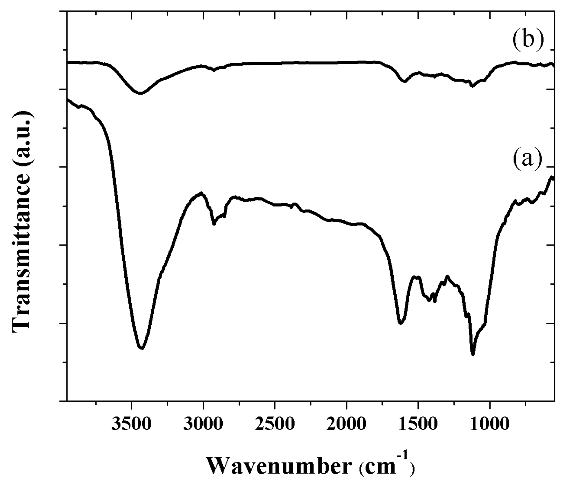
3.1. Raman and FT-IR Characterization

According to Raman analysis, thermal processing at 1000 °C under an Ar atmosphere produced the simultaneous formation of the silicon nanoparticles or carbon–silicon nanowires and GO reduction. Similar results regarding the reduction level and the silicon–silicon carbide nanoparticles formation were obtained for both samples, A and B.
Figure 1 shows Raman spectrum (sample B) of (a) as-deposited GO and (b) one corresponding to GO–Si hybrid nanocomposite on the Si substrate. The as-deposited GO Raman spectrum exhibits the G and D bands at 1598 and 1357 cm−1, respectively. As frequently reported, they originate from the in-plane vibrations of carbon sp2 bonds (G band), and structural defects (D band) [36,37]. After the thermal process (Figure 1b), both bands changed in position and intensity, consistently with the GO reduction degree [38]. That is, the G and D peaks underwent a red-shift of about 13 and 10 cm−1, respectively. The red shift of the G band suggests the reduction of graphene oxide and the recovery of the sp2 domain, while the D band shift is associated with the size of the in-plane sp2 domain [37,39]. Likewise, the increase in the I(D)/I(G) ratio from 0.91 to 1.21 indicates the formation of numerous aromatic domains of smaller overall size in graphene [40]. Note that Chan Lee et al. [41] reported the effective reduction of sprayed-GO films by Si.
Raman spectrum of rGO-Si nanocomposite (Figure 1b) displays the GO Raman bands and those belonging to silicon ~515 and 950 cm−1. The sharp band at 515 cm−1 could be assigned to TO vibration of Si–Si bond [42], the red shift from the assigned value of bulk silicon (~520 cm−1) could be attributed to the presence of nanocrystals in the nanowire [43]. The low intensity Raman band at 950 cm−1 appears to correspond to nanosized silicon, as reported by Meier et al. [44], however, the HR-TEM analysis of prepared material revealed that polycrystalline nanoparticles composed of Si and SiC were obtained.
On the other hand, the FT-IR characterization served to confirm the effective GO reduction as indicated by Raman spectroscopy. As-deposited GO (Figure 2a) shows absorption bands at 1117, 1201, 1427, 1622, and 3425 cm−1, corresponding to C–O stretching vibrations, C–OH stretching vibrations, O–H deformation, C=C stretching (skeletal vibrations from unoxidized graphitic domains), and O–H stretching vibrations, respectively, all of them in good agreement with the wavenumber localization reported for GO prepared by the Hummers’ method [45,46].
The FT-IR spectrum of GO–Si nanoparticle composite (Figure 2b) also suggests the reduction of thermally processed GO with the temperature, since all the absorption bands associated with the abovementioned oxygenated groups decreased in intensity. It was even observed that the thermal process led to the entire vanishing of some bands. In the FT-IR spectra, both of the silicon nanoparticles and of the carbon and silicon nanowires, the bands associated to Si–C or Si–O cannot be appreciated in Figure 2b, since the signals are screened, due to the core–shell structure [47].

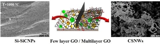
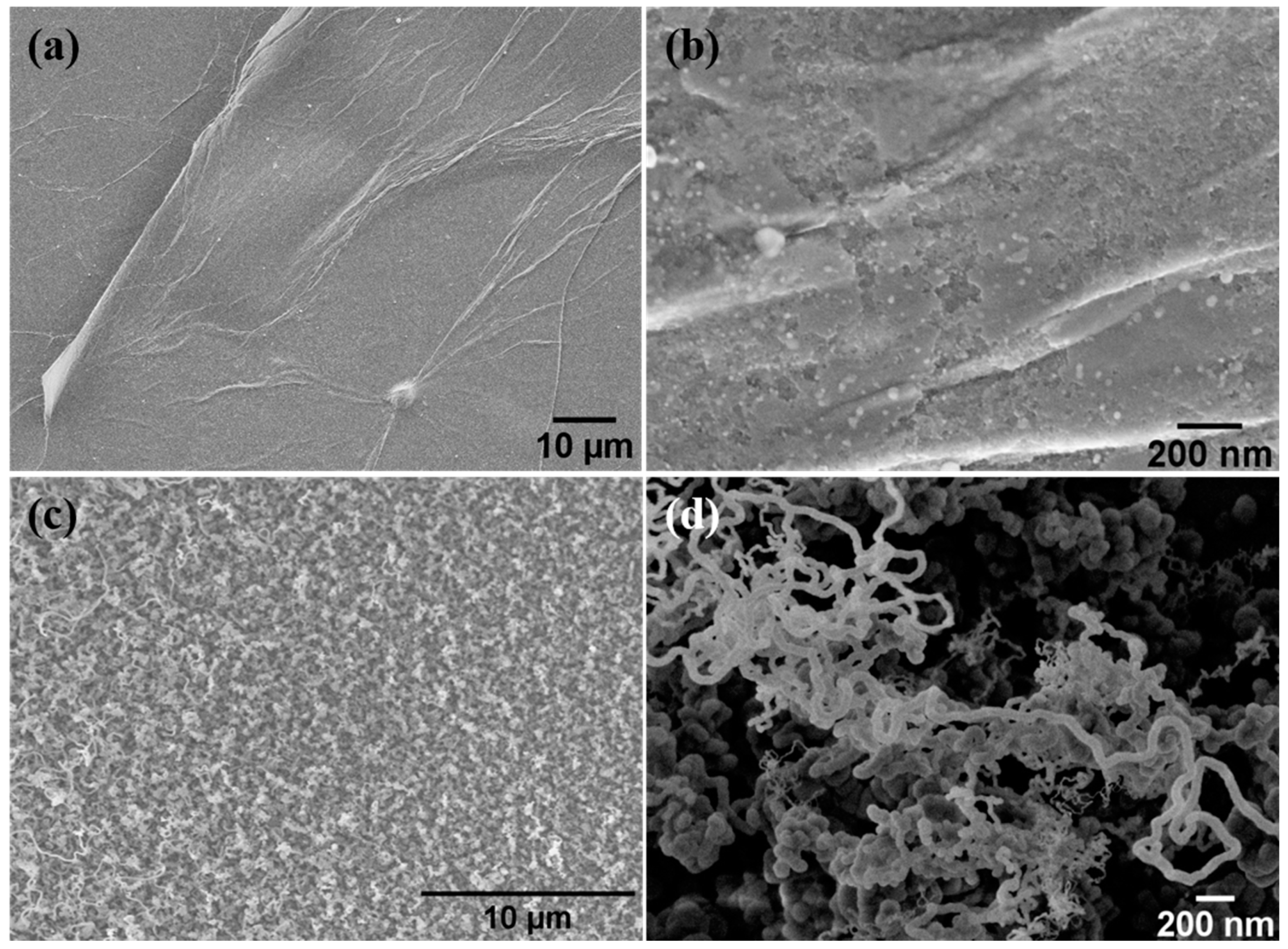
3.2. Morphology and Structure

After being prepared, the structure and morphology of samples A and B were examined by FE-SEM and HR-TEM. It was found that the thermal annealing led to the formation of silicon-derived nanoparticles at the GO/Si interface, and their morphology and mean particle size strongly depended on the GO film thickness. The HR-TEM analysis revealed that the nanoparticles are multiphase, comprising Si and SiC as dominant phases. The sample A (GO film thickness of around 100 nm) consists of Si–SiC nanoparticles of 20 nm mean size decorating the GO sheet surface (Figure 3a,b). On the other hand, in sample B (GO film thickness of 1 μm), Si–SiC nanoparticles (30 nm mean size) were self-assembled into worm-like hybrid nanostructures, as shown in the FE-SEM images at low- and high-magnification (Figure 3c,d, respectively). These hybrid rGO-Si–SiC worm-like nanostructures are mostly 10–100 nm in diameter with a length of several micrometers, covering a relatively large area of the Si wafer surface (note the magnitude scale of FE-SEM image in Figure 3d).
The TEM and HRTEM images in Figure 4 display the morphological features of samples A and B. Figure 4a corroborates the FE-SEM characterization result in that Si-based nanoparticles decorate the rGO sheets in the sample A. On the other hand, Figure 4c,d displays the striking morphology of sample B, which consists of different-sized nanoparticles that self-assembled to develop the worm-like structures, as those shown in Figure 3d. TEM images, Figure 4c,d, suggest that silicon-derived nanoparticles are embedded into 1D self-assembled rGO sheets. In Figure 4d, a magnified image of the framed zone in Figure 4b is shown. It provides a more detailed view of the branched characteristics of the worm-like nanostructures, as they are formed by rGO-supported individual nanoparticles.
The HR-TEM images of individual nanoparticles of samples A and B are shown in Figure 4b,e, respectively. It is seen that both are 30 nm diameter ball-shaped nanoparticles, apparently coated with an rGO shell. A careful determination of interplanar spacing revealed that various crystalline phases coexist in the formed nanoparticles, that is, they are multiphase polycrystalline entities; geometric shapes in Figure 4c were used to indicate the coexisting crystalline phases.
We report fast Fourier Transform (FTT) images in the inset of Figure 4b, and the areas selected in Figure 4c were used to estimate interplanar distances, which agree well with that reported for the spacing of (100), (002), (110), (111), and (131) planes of cubic SiC, (111), (113), and (353) of Si, and (110), (011), (302), and (300) of graphite (C). Note that, if they exist, we were unable to detect silicon oxide-derived phases.

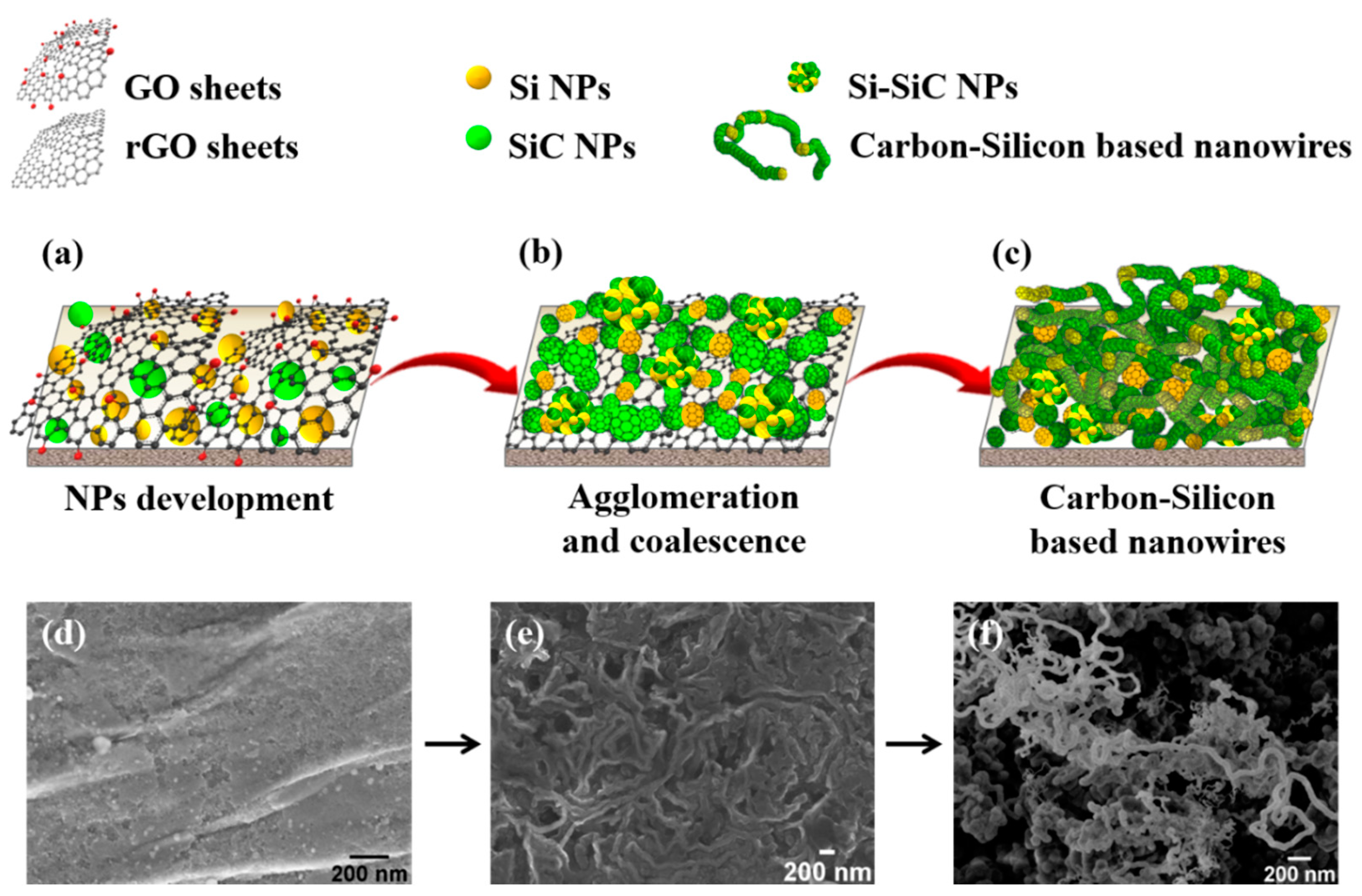
3.3. Mechanism Proposed for the CSNW Formation

The morphological characterization by FE-SEM and HR-TEM suggests that polycrystalline Si–SiC nanoparticles arise as the primary building blocks to develop more complex nanostructures. Both the mean particle size and morphology are strongly associated to the GO film thickness. Indeed, experiments carried out on silicon wafer GO-free surface were unsuccessful in growing silicon nanoparticles. After being formed, they interact, leading to a self-assembly process that produces the worm-like structures.
To explain the silicon nanoparticle formation, we have assumed that they originate from melted silicon at the silicon surface through a nucleation process that starts at the high energy edges of GO sheets. Since the Si melting point is around 1414 °C [48], and the hybrid materials were made at 1000 °C, we proposed that impurities and structural defects at the silicon wafer surface might promote the melting of silicon surface (pre-melting effect) at temperatures lower than the nominal silicon melting point. Also, it is quite probable that GO has a certain participation in the melting of silicon surface, because recent reports suggest that GO could act as a high temperature reactor [49]. Thus, we believe that the synergy between the pre-melting effect and the ability of GO to absorb IR radiation [50] promotes melting of the silicon surface. Additional support for the silicon surface pre-melting at temperatures lower than its melting point is provided by the roughness change observed in thermal oxidation at the silicon wafer surface, at temperatures of 900–1000 °C [51,52,53].
Regarding the phase composition of nanoparticles, it is known that the temperature of GO pyrolysis strongly depends on GO sheet size. It is quite probable that the combined participation of both GO pyrolysis and CO2 emission by GO reduction supply elemental carbon to react with silicon and, in so doing, form the observed silicon carbide. The formed nanoparticles are stabilized by the rGO network.
Accordingly, we propose that the observed worm-like hybrid nanostructures develop as illustrated in Figure 5.
At first, small Si–SiC nanoparticles develop (Figure 5a), then, they diffuse across the melted silicon surface to interact and, finally, they coalesce to form larger nanostructures (Figure 5b). The worm-like structure originates from the GO-promoted self-assembly of individual Si, SiC, and Si–SiC polycrystalline nanoparticles, with the latter formed by the coalescence among Si and SiC (see Figure 5c), as suggested by HR-TEM (Figure 4). The FE-SEM images (Figure 5d–f) were added to support the proposed mechanism for the nanoparticle self-assembly.

4. Conclusions

In summary, we have presented the development of silicon–silicon carbide (Si–SiC) nanoparticles at the graphene oxide/silicon interface. Depending on the GO film thickness, the obtained nanoparticles disperse on the silicon surface, or they self-assemble into a few-micrometer 1D worm-like hybrid nanostructure. It was demonstrated that dispersed silicon nanoparticles develop on graphene oxide layers, whilst 1D nanostructures comprise GO-embedded self-assembled Si–SiC nanoparticles. It was assumed that the silicon surface melts, and that Si and SiC nanoparticles originated through a graphene oxide-induced nucleation of melted silicon. In addition, a mechanism for the formation of the (CSNW) was proposed.

Author Contributions

M.A.P.-G. and R.O.-A. participated in the conceptualization, investigation, and writing draft preparation, Y.M. and A.M.E.-R. participated in the methodology, validation, writing draft, and editing, J.M.-C. and J.S.-S. had participated in the data curation and writing review and editing, M.O.-L. participated in the conceptualization, supervision, and writing review and editing.

Funding

This research received no external funding.

Acknowledgments

This project is supported by the National Council of Science and Technology (CONACyT) scholarships Nos. 354945 (M.A.P.-G.) and 355201 (R.O.-A.). The authors are very thankful to Daniel Bahena Uribe for his valuable assistance for HR-TEM characterization and Jorge Roque De la Puente Ibarra for the FE-SEM images, both from LANE-Cinvestav. We are also grateful to Arturo Ponce-Pedraza from Physics Department and to the Kleberg Advanced Microscopy Center, University of Texas at San Antonio, for FE-SEM characterization. Finally, we would like to thank to Miguel Luna Arias from SEES, Cinvestav, for the profilometer measurements.

Conflicts of Interest

The authors declare no conflict of interest.

References

  1. Ghosh, B.; Sarma, S.; Pontsho, M.; Ray, S.C. Tuning of magnetic behaviour in nitrogenated graphene oxide functionalized with iron oxide. Diam. Relat. Mater. 2018, 89, 35–42. [Google Scholar] [CrossRef]
  2. Velasco-Soto, M.A.; Pérez-García, S.A.; Alvarez-Quintana, J.; Cao, Y.; Nyborg, L.; Licea-Jiménez, L. Selective band gap manipulation of graphene oxide by its reduction with mild reagents. Carbon 2015, 93, 967–973. [Google Scholar] [CrossRef]
  3. Wang, R.; Lu, K.-Q.; Tang, Z.-R.; Xu, Y.-J. Recent progress in carbon quantum dots: Synthesis, properties and applications in photocatalysis. J. Mater. Chem. A 2017, 5, 3717–3734. [Google Scholar] [CrossRef]
  4. Lucien, R.; Sunjie, Y.; Samuel, C.T.M.; Kevin, C.; Coletta, P.L.; Stephen, D.E. Morphological control of seedlessly-synthesized gold nanorods using binary surfactants. Nanotechnology 2018, 29, 135601. [Google Scholar] [Green Version]
  5. Zhu, K.; Ju, Y.; Xu, J.; Yang, Z.; Gao, S.; Hou, Y. Magnetic Nanomaterials: Chemical Design, Synthesis, and Potential Applications. Acc. Chem. Res. 2018, 51, 404–413. [Google Scholar] [CrossRef] [PubMed]
  6. Chen, F.; Hableel, G.; Zhao, E.R.; Jokerst, J.V. Multifunctional nanomedicine with silica: Role of silica in nanoparticles for theranostic, imaging, and drug monitoring. J. Colloid Interface Sci. 2018, 521, 261–279. [Google Scholar] [CrossRef] [PubMed]
  7. Wu, Z.-S.; Zhou, G.; Yin, L.-C.; Ren, W.; Li, F.; Cheng, H.-M. Graphene/metal oxide composite electrode materials for energy storage. Nano Energy 2012, 1, 107–131. [Google Scholar] [CrossRef]
  8. Thomas, V.J.; Ramaswamy, S. Application of Graphene and Graphene Compounds for Environmental Remediation. Sci. Adv. Mater. 2016, 8, 477–500. [Google Scholar] [CrossRef]
  9. Bai, S.; Shen, X. Graphene-inorganic nanocomposites. RSC Adv. 2012, 2, 64–98. [Google Scholar] [CrossRef]
  10. Huang, J.; Li, Y.; Jia, X.; Song, H. Preparation and tribological properties of core–shell Fe3O4@C microspheres. Tribol. Int. 2019, 129, 427–435. [Google Scholar] [CrossRef]
  11. Hou, L.; Zheng, H.; Cui, R.; Jiang, Y.; Li, Q.; Jiang, X.; Gao, J.; Gao, F. Silicon carbon nanohybrids with expandable space: A high-performance lithium battery anodes. Microporous Mesoporous Mater. 2019, 275, 42–49. [Google Scholar] [CrossRef]
  12. Hong, W.G.; Kim, B.H.; Lee, S.M.; Yu, H.Y.; Yun, Y.J.; Jun, Y.; Lee, J.B.; Kim, H.J. Agent-free synthesis of graphene oxide/transition metal oxide composites and its application for hydrogen storage. Int. J. Hydrogen Energy 2012, 37, 7594–7599. [Google Scholar] [CrossRef]
  13. Sarkar, S.; Howli, P.; Das, B.; Das, N.S.; Samanta, M.; Das, G.C.; Chattopadhyay, K.K. Novel Quaternary Chalcogenide/Reduced Graphene Oxide-Based Asymmetric Supercapacitor with High Energy Density. ACS Appl. Mater. Interfaces 2017, 9, 22652–22664. [Google Scholar] [CrossRef] [PubMed]
  14. Piao, S.H.; Choi, H.J. Smart Graphene Oxide Based Composite Materials and their Electric and Magnetic Stimuli-response. Procedia Eng. 2017, 171, 64–70. [Google Scholar] [CrossRef]
  15. Sun, S.; Zhou, A.; Gu, D.; Hu, X.; Li, Z.; Chen, L.; Ma, C.; Dong, L.; Yin, Y.; Chang, X. A general strategy for the synthesis of reduced graphene oxide-based composites. Ceram. Int. 2015, 41, 7661–7668. [Google Scholar] [CrossRef]
  16. Ge, M.; Rong, J.; Fang, X.; Zhang, A.; Lu, Y.; Zhou, C. Scalable preparation of porous silicon nanoparticles and their application for lithium-ion battery anodes. Nano Res. 2013, 6, 174–181. [Google Scholar] [CrossRef]
  17. Miyano, M.; Endo, S.; Takenouchi, H.; Nakamura, S.; Iwabuti, Y.; Shiino, O.; Nakanishi, T.; Hasegawa, Y. Novel Synthesis and Effective Surface Protection of Air-Stable Luminescent Silicon Nanoparticles. J. Phys. Chem. C 2014, 118, 19778–19784. [Google Scholar] [CrossRef]
  18. Lal, S.; Caseley, E.A.; Hall, R.M.; Tipper, J.L. Biological Impact of Silicon Nitride for Orthopaedic Applications: Role of Particle Size, Surface Composition and Donor Variation. Sci. Rep. 2018, 8, 9109. [Google Scholar] [CrossRef] [PubMed]
  19. Ege, D.; Kamali, A.R.; Boccaccini, A.R. Graphene Oxide/Polymer-Based Biomaterials. Adv. Eng. Mater. 2017, 19, 1700627. [Google Scholar] [CrossRef] [Green Version]
  20. O’Farrell, N.; Houlton, A.; Horrocks, B.R. Silicon nanoparticles: Applications in cell biology and medicine. Int. J. Nanomed. 2006, 1, 451–472. [Google Scholar] [CrossRef]
  21. Su, S.; He, Y.; Zhang, M.; Yang, K.; Song, S.; Zhang, X.; Fan, C.; Lee, S.-T. High-sensitivity pesticide detection via silicon nanowires-supported acetylcholinesterase-based electrochemical sensors. Appl. Phys. Lett. 2008, 93, 023113. [Google Scholar] [CrossRef]
  22. Arunmetha, S.; Vinoth, M.; Srither, S.R.; Karthik, A.; Sridharpanday, M.; Suriyaprabha, R.; Manivasakan, P.; Rajendran, V. Study on Production of Silicon Nanoparticles from Quartz Sand for Hybrid Solar Cell Applications. J. Electron. Mater. 2018, 47, 493–502. [Google Scholar] [CrossRef]
  23. Zywietz, U.; Evlyukhin, A.B.; Reinhardt, C.; Chichkov, B.N. Laser printing of silicon nanoparticles with resonant optical electric and magnetic responses. Nat. Commun. 2014, 5, 3402. [Google Scholar] [CrossRef] [PubMed] [Green Version]
  24. Garín, M.; Fenollosa, R.; Alcubilla, R.; Shi, L.; Marsal, L.F.; Meseguer, F. All-silicon spherical-Mie-resonator photodiode with spectral response in the infrared region. Nat. Commun. 2014, 5, 3440. [Google Scholar] [CrossRef] [PubMed] [Green Version]
  25. Shavel, A.; Guerrini, L.; Alvarez-Puebla, R.A. Colloidal synthesis of silicon nanoparticles in molten salts. Nanoscale 2017, 9, 8157–8163. [Google Scholar] [CrossRef] [PubMed]
  26. Shen, C.; Barrios, E.; Zhai, L. Bulk Polymer-Derived Ceramic Composites of Graphene Oxide. ACS Omega 2018, 3, 4006–4016. [Google Scholar] [CrossRef]
  27. Jeong, M.-G.; Du, H.L.; Islam, M.; Lee, J.K.; Sun, Y.-K.; Jung, H.-G. Self-Rearrangement of Silicon Nanoparticles Embedded in Micro-Carbon Sphere Framework for High-Energy and Long-Life Lithium-Ion Batteries. Nano Lett. 2017, 17, 5600–5606. [Google Scholar] [CrossRef] [PubMed]
  28. Chen, Y.; Hu, Y.; Shen, Z.; Chen, R.; He, X.; Zhang, X.; Li, Y.; Wu, K. Hollow core–shell structured silicon@carbon nanoparticles embed in carbon nanofibers as binder-free anodes for lithium-ion batteries. J. Power Sources 2017, 342, 467–475. [Google Scholar] [CrossRef]
  29. Huang, R.; Fan, X.; Shen, W.; Zhu, J. Carbon-coated silicon nanowire array films for high-performance lithium-ion battery anodes. Appl. Phys. Lett. 2009, 95, 133119. [Google Scholar] [CrossRef]
  30. Wang, J.; Fan, F.; Liu, Y.; Jungjohann, K.L.; Lee, S.W.; Mao, S.X.; Liu, X.; Zhu, T. Structural Evolution and Pulverization of Tin Nanoparticles during Lithiation-Delithiation Cycling. J. Electrochem. Soc. 2014, 161, F3019–F3024. [Google Scholar] [CrossRef]
  31. Gribov, B.G.; Zinov’ev, K.V.; Kalashnik, O.N.; Gerasimenko, N.N.; Smirnov, D.I.; Sukhanov, V.N.; Kononov, N.N.; Dorofeev, S.G. Production of Silicon Nanoparticles for Use in Solar Cells. Semiconductors 2017, 51, 1675–1680. [Google Scholar] [CrossRef]
  32. Zyuzin, M.V.; Baranov, D.G.; Escudero, A.; Chakraborty, I.; Tsypkin, A.; Ushakova, E.V.; Kraus, F.; Parak, W.J.; Makarov, S.V. Photoluminescence quenching of dye molecules near a resonant silicon nanoparticle. Sci. Rep. 2018, 8, 6107. [Google Scholar] [CrossRef] [PubMed]
  33. Hardman, R. A Toxicologic Review of Quantum Dots: Toxicity Depends on Physicochemical and Environmental Factors. Environ. Health Perspect. 2006, 114, 165–172. [Google Scholar] [CrossRef] [PubMed]
  34. Ortega-Amaya, R.; Matsumoto, Y.; Flores-Conde, A.; Pérez-Guzmán, M.A.; Ortega-López, M. In situ formation of rGO quantum dots during GO reduction via interaction with citric acid in aqueous medium. Mater. Res. Express 2016, 3, 105601. [Google Scholar] [CrossRef]
  35. Ortega-Amaya, R.; Matsumoto, Y.; Pérez-Guzmán, M.A.; Ortega-López, M. In situ synthesis of Cu2O and Cu nanoparticles during the thermal reduction of copper foil-supported graphene oxide. J. Nanopart. Res. 2015, 17, 397. [Google Scholar] [CrossRef]
  36. Sobon, G.; Sotor, J.; Jagiello, J.; Kozinski, R.; Zdrojek, M.; Holdynski, M.; Paletko, P.; Boguslawski, J.; Lipinska, L.; Abramski, K.M. Graphene Oxide vs. Reduced Graphene Oxide as saturable absorbers for Er-doped passively mode-locked fiber laser. Opt. Express 2012, 20, 19463–19473. [Google Scholar] [CrossRef] [PubMed]
  37. Chen, W.; Yan, L. Preparation of graphene by a low-temperature thermal reduction at atmosphere pressure. Nanoscale 2010, 2, 559–563. [Google Scholar] [CrossRef] [PubMed]
  38. Ji, Z.; Shen, X.; Li, M.; Zhou, H.; Zhu, G.; Chen, K. Synthesis of reduced graphene oxide/CeO2 nanocomposites and their photocatalytic properties. Nanotechnology 2013, 24, 115603. [Google Scholar] [CrossRef] [PubMed]
  39. Zhang, Y.; Ma, H.-L.; Zhang, Q.; Peng, J.; Li, J.; Zhai, M.; Yu, Z.-Z. Facile synthesis of well-dispersed graphene by [gamma]-ray induced reduction of graphene oxide. J. Mater. Chem. 2012, 22, 13064–13069. [Google Scholar] [CrossRef]
  40. Stankovich, S.; Dikin, D.A.; Piner, R.D.; Kohlhaas, K.A.; Kleinhammes, A.; Jia, Y.; Wu, Y.; Nguyen, S.T.; Ruoff, R.S. Synthesis of graphene-based nanosheets via chemical reduction of exfoliated graphite oxide. Carbon 2007, 45, 1558–1565. [Google Scholar] [CrossRef]
  41. Chan Lee, S.; Some, S.; Wook Kim, S.; Jun Kim, S.; Seo, J.; Lee, J.; Lee, T.; Ahn, J.-H.; Choi, H.-J.; Chan Jun, S. Efficient Direct Reduction of Graphene Oxide by Silicon Substrate. Sci. Rep. 2015, 5, 12306. [Google Scholar] [CrossRef] [PubMed]
  42. Kole, A.; Chaudhuri, P. Growth of silicon quantum dots by oxidation of the silicon nanocrystals embedded within silicon carbide matrix. AIP Adv. 2014, 4, 107106. [Google Scholar] [CrossRef] [Green Version]
  43. Parul, S.; Anguita, J.V.; Stolojan, V.; Henley, S.J.; Silva, S.R.P. The growth of silica and silica-clad nanowires using a solid-state reaction mechanism on Ti, Ni and SiO2 layers. Nanotechnology 2010, 21, 295603. [Google Scholar]
  44. Meier, C.; Lüttjohann, S.; Kravets, V.G.; Nienhaus, H.; Lorke, A.; Wiggers, H. Raman properties of silicon nanoparticles. Phys. E Low-Dimens. Syst. Nanostruct. 2006, 32, 155–158. [Google Scholar] [CrossRef]
  45. Dong, J.; Liu, W.; Li, H.; Su, X.; Tang, X.; Uher, C. In situ synthesis and thermoelectric properties of PbTe-graphene nanocomposites by utilizing a facile and novel wet chemical method. J. Mater. Chem. A 2013, 1, 12503–12511. [Google Scholar] [CrossRef]
  46. Shen, J.; Yan, B.; Shi, M.; Ma, H.; Li, N.; Ye, M. One step hydrothermal synthesis of TiO2-reduced graphene oxide sheets. J. Mater. Chem. 2011, 21, 3415–3421. [Google Scholar] [CrossRef]
  47. Necmi, S.; Tülay, S.; Şeyda, H.; Yasemin, Ç. Annealing effects on the properties of copper oxide thin films prepared by chemical deposition. Semicond. Sci. Technol. 2005, 20, 398. [Google Scholar]
  48. Durand, F.; Duby, J.C. Carbon solubility in solid and liquid silicon—A review with reference to eutectic equilibrium. J. Phase Equilib. 1999, 20, 61. [Google Scholar] [CrossRef]
  49. Barman, B.K.; Nanda, K.K. Ultrafast-Versatile-Domestic-Microwave-Oven Based Graphene Oxide Reactor for the Synthesis of Highly Efficient Graphene Based Hybrid Electrocatalysts. ACS Sustain. Chem. Eng. 2018, 6, 4037–4045. [Google Scholar] [CrossRef]
  50. Bae, J.J.; Yoon, J.H.; Jeong, S.; Moon, B.H.; Han, J.T.; Jeong, H.J.; Lee, G.-W.; Hwang, H.R.; Lee, Y.H.; Jeong, S.Y.; et al. Sensitive photo-thermal response of graphene oxide for mid-infrared detection. Nanoscale 2015, 7, 15695–15700. [Google Scholar] [CrossRef] [PubMed]
  51. Araki, K.; Takeda, R.; Sudo, H.; Izunome, K.; Zhao, X. Dependence of Atomic-Scale Si(110) Surface Roughness on Hydrogen Introduction Temperature after High-Temperature Ar Annealing. J. Surf. Eng. Mater. Adv. Technol. 2014, 4, 249–256. [Google Scholar] [CrossRef]
  52. Shive, L.W.; Gilmore, B.L. Impact of Thermal Processing on Silicon Wafer Surface Roughness. ECS Trans. 2008, 16, 401–405. [Google Scholar]
  53. Shi, Z.; Shao, S.; Wang, Y. Improved the Surface Roughness of Silicon Nanophotonic Devices by Thermal Oxidation Method. J. Phys. Conf. Ser. 2011, 276, 012087. [Google Scholar] [CrossRef] [Green Version]
Figure 1. Raman spectra of as-deposited graphene oxide (GO) (a) and reduced graphene oxide (rGO)-Si hybrid nanocomposite (b). The latter displays Raman bands of Si (namely, the substrate) at 515 cm−1 and nanosized Si at 950 cm−1.
Nanomaterials 08 00954 g001
Figure 2. FT-IR spectra of (a) as-deposited GO and annealed sample at (b) 1000 °C for 1 h.
Nanomaterials 08 00954 g002
Figure 3. FE-SEM images of sample A (a,b) (nanoparticles decorating rGO sheets) and sample B (c,d) (the CSNW obtained from the thermal annealing of the GO at 1000 °C, using a Si wafer as support).
Nanomaterials 08 00954 g003
Figure 4. TEM and HR-TEM images of the sample A (a,b) and the sample B (ce) after thermal annealing of GO at 1000 °C. (a) rGO sheets decorated by Si-based polydispersed nanoparticles. (b) HR-TEM of an irregularly shaped nanoparticle, where the inset corresponds to the FTT of (b). (c,d) Images of carbon–silicon-based nanowires (CSNW) which consist of Si-based nanoparticles embedded into 1D self-assembled rGO sheets. (e) HR-TEM of a nanoparticle, where it can be observed that it is polycrystalline. (f) The FTT of selected areas in (e).
Nanomaterials 08 00954 g004
Figure 5. Scheme of the proposed mechanism for the carbon–silicon-based nanowires formation. (a) Si-based nanoparticle development at the interface GO and Si wafer. (b) nanoparticle agglomeration and coalescence into larger structures. (c) carbon-silicon based nanowires formation. FE-SEM images to support the proposed steps (d) development. (e) agglomeration and coalescence and (f) carbon-silicon based nanowires formation.
Nanomaterials 08 00954 g005

