Article

Fabrication of InxGa1−xN Nanowires on Tantalum Substrates by Vapor-Liquid-Solid Chemical Vapor Deposition

1
Fujian Provincial Key Laboratory of Functional Materials and Applications, School of Materials Science and Engineering, Xiamen University of Technology, Xiamen 361024, China
2
TJU-NIMS International Collaboration Laboratory, School of Materials Science and Engineering, Tianjin University, Nankai District, Tianjin 300072, China
*
Author to whom correspondence should be addressed.
Nanomaterials 2018, 8(12), 990; https://doi.org/10.3390/nano8120990
Submission received: 5 November 2018 / Revised: 23 November 2018 / Accepted: 27 November 2018 / Published: 29 November 2018

Abstract

:
InxGa1−xN nanowires (NWs) have drawn great attentions for their applications in optoelectronic and energy conversion devices. Compared to conventional substrates, metal substrates can offer InxGa1−xN NW devices with better thermal conductivity, electric conductivity, and mechanic flexibility. In this article, InxGa1−xN NWs were successfully grown on the surface of a tantalum (Ta) substrate via vapor-liquid-solid chemical vapor deposition (VLS-CVD), as characterized by X-ray diffraction (XRD), scanning electron microscope (SEM), scanning and transmission electron microscope (STEM), and photoluminescence spectroscopy (PL). It was found that the surface pretreatment of Ta and the composition of metallic catalysts played important roles in the formation of NWs. A dimpled nitrided Ta surface combined with a catalyst of nickle is suitable for VLS-CVD growth of the NWs. The obtained InxGa1−xN NWs grew along the [1100] direction with the presence of basal stacking faults and an enriched indium composition of ~3 at.%. The successful VLS-CVD preparation of InxGa1−xN nanowires on Ta substrates could pave the way for the large-scale manufacture of optoelectronic devices in a more cost-effective way.

1. Introduction

InxGa1−xN alloys are important optoelectronic materials, which have been widely used in light emitting diodes and laser diodes due to their tunable band-gaps [1]. InxGa1−xN alloys are also very promising for energy conversion applications such as solar water splitting [2], photocatalytic reduction of CO2 [3], lithium ion batteries [4], and supercapacitors [5]. InxGa1−xN nanowires (NWs), especially, have drawn great attention due to their large surface area and improved carrier collection efficiency. A variety of InxGa1−xN NW devices have been prepared and exhibited excellent performances [6,7,8,9,10]. Another advantage of InxGa1−xN NWs is that they can accommodate lateral lattice mismatch with the substrate and, therefore, suppress the formation of threading dislocations. Other than conventional substrates such as sapphire, SiC, and Si, InxGa1−xN NWs have been successfully grown on Ti [11,12], Mo [13], Ta [14], Hf [15], Ni [16], copper [17], stainless steel [18], carbon paper [4,5], etc. [19]. These new substrates have offered the InxGa1−xN NW devices with better thermal conductivity, electric conductivity, and mechanic flexibility. Most of these growths were implemented by molecular beam epitaxy (MBE) or metallorganic chemical vapour deposition (MOCVD). Compared to MBE and MOCVD, chemical vapor deposition (CVD) is less expensive, making it more attractive to fabricate large-area devices at a lower cost.
In this article, a vapor-liquid-solid (VLS)-CVD technique was employed to grow InxGa1−xN NWs on a pure tantalum (Ta) substrate. Ta was chosen as a substrate based on the fact that after CVD growth Ta surface would form tantalum oxides, oxynitrides, and tantalum nitrides, such as Ta2O5, TaON, Ta3N5, and TaxNy subnitrides. These tantalum oxides or nitrides are either conductive themselves, or have matched energy band structures with InxGa1−xN. Ta2O5, for example, is a potential coating material, catalyst, capacitor, resistor, and optical device itself. Ta2O5 can be synthesized by thermal oxidation or electrochemically anodic oxidation [20,21]. Electrochemical anodic oxidation of Ta has been carried out to obtain a highly ordered dimpled Ta surface as a template for Au nanoparticle arrays [22], which can be used as catalyst arrays for VLS-CVD growth of nanowires. Furthermore, ammonolysis of Ta2O5 can achieve TaON and Ta3N5, both of which are promising visible-light photocatalysts [23,24]. Besides, Ta2O5, TaON, and Ta3N5 all have matched energy band structures with InxGa1−xN [25]. Nitridation of the Ta2O5 film would also result in TaxNy subnitrides, which can work as conductive layers between the film and the Ta substrate [26]. Based on the above analysis, we employed both thermal oxidation and electrochemical oxidation to obtain Ta2O5 films on the surfaces of the Ta substrates. After a post-nitridation process, CVD growth of InxGa1−xN NWs was carried out on the surface of the Ta substrates. It was found that InxGa1−xN NWs can only be successfully fabricated on a specifically pretreated tantalum surface when Ni-Au alloys with certain compositions were used as catalysts. The microstructures of the obtained InxGa1−xN NWs/Ta samples were extensively characterized.

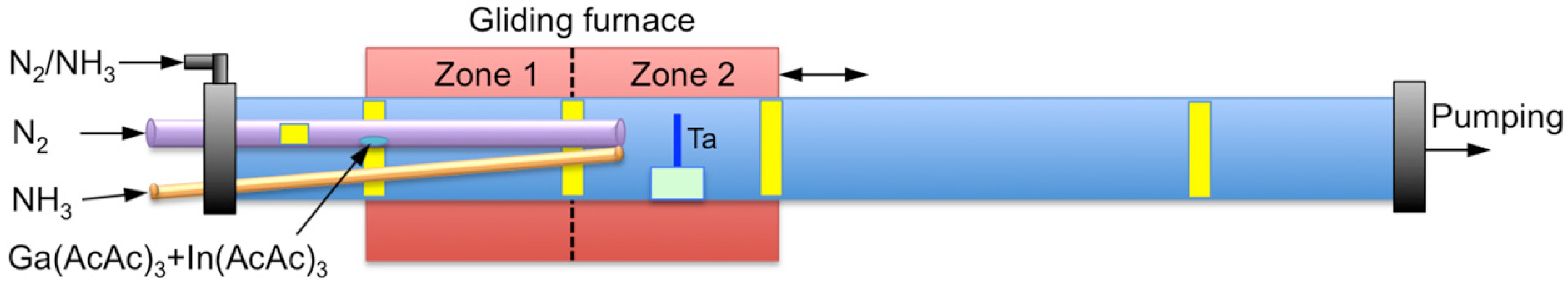
2. Materials and Methods

Three surface states of polished Ta (99.95 %) plates were employed as substrates for the NWs growth: native, oxidative, and nitrided. Oxidative state was obtained by the heat-treatment of the polished Ta plates under atmosphere at 500 °C for 4 h. Nitrided Ta surface was achieved by a high voltage anodization followed by a high temperature nitridation. The polished Ta plates were electrochemically anodized in a two-electrode system using a platinum foil (10 × 10 mm) as the counter-electrode. The anodization was operated at 80 V in a stirred solution of concentrated H2SO4 (95–98%), H2O, and HF (48%) in a volume ratio of 9:4:1 for around 5–10 min until the oxide film was peeled off. The residue white films were further removed by sonication in the deionized water. The samples were then nitridated at 950 °C under 1 atm for 2 h with NH3 of 100 standard-state cubic centimetres per minute (sccm).
The treated tantalum plates were then coated with mixed salts of Ni(NO3)2 and HAuCl4·4H2O as catalysts, with a volumetric percentage of the Ni(NO3)2 ethanol solution as 100%, 50%, 33.3%, 20%, and 0%, respectively. The catalysts were specified as Ni, Ni1Au1, Ni1Au2, Ni1Au4, and Au, accordingly. The treated tantalum plates with catalysts were dried at 40 °C in air before CVD growth.
The CVD growth was carried out in a horizontal gliding furnace as shown in Figure 1 to realize fast heating and cooling. A mixture of gallium acetylacetonate (Ga(AcAc)3) and indium acetylacetonate (In(AcAc)3) (99.99%) were used as the metallic precursors to react with NH3 to produce InxGa1−xN NWs [27]. The furnace has two heating zones, which were set as 400 °C and 800 °C, respectively. When the desired temperatures were attained, the furnace was glided from right to the left to align the edge of zone 1 with the metallic source, which is a mixture of 0.15 g Ga(AcAc)3 and 0.06 g In(AcAc)3. The center of zone 2 would correspond to the location of the treated Ta plate. H2 (20 sccm) was introduced to reduce Ni catalyst when the temperature was ramping up. Once the desired temperatures were recovered, H2 was turned off and N2 (20 sccm) was used as a carrier gas along an inner quartz tube (Φ30 mm) to transport metallic precursors to react with NH3 (80 sccm), which flowed through a separate inner quartz tube (Φ10 mm) to prevent parasitic reactions. The pressure was kept as 2000 Pa for 30 min. Upon the completion of the CVD growth, the furnace was glided away, and N2 and NH3 were switched to the outer quartz tube (Φ100 mm) to accelerate the cooling process.
The morphologies of the obtained samples were examined using a field emission scanning electron microscope (SEM, Zeiss Sigma 500, Netherland). The structures were identified by X-ray diffraction (XRD, Philips, PANalytical X’pert, Netherland, Cu Ka radiation (λ = 1.5417 Å)). The microstrucutre characterization of the obtained NWs was performed with Transmission Electron Microscope (TEM) using a TEM/STEM system (FEI Talos F200X, Hillsboro, OR, USA) equipped with 2 Super-X SDDs. Low temperature photoluminescence (RT-PL) was performed at 77 K with an excited wavelength of 267 nm (Horiba JobinYvon Fluorlog 3-21, USA) to evaluate the optical properties of the obtained NWs.

3. Results and Discussion

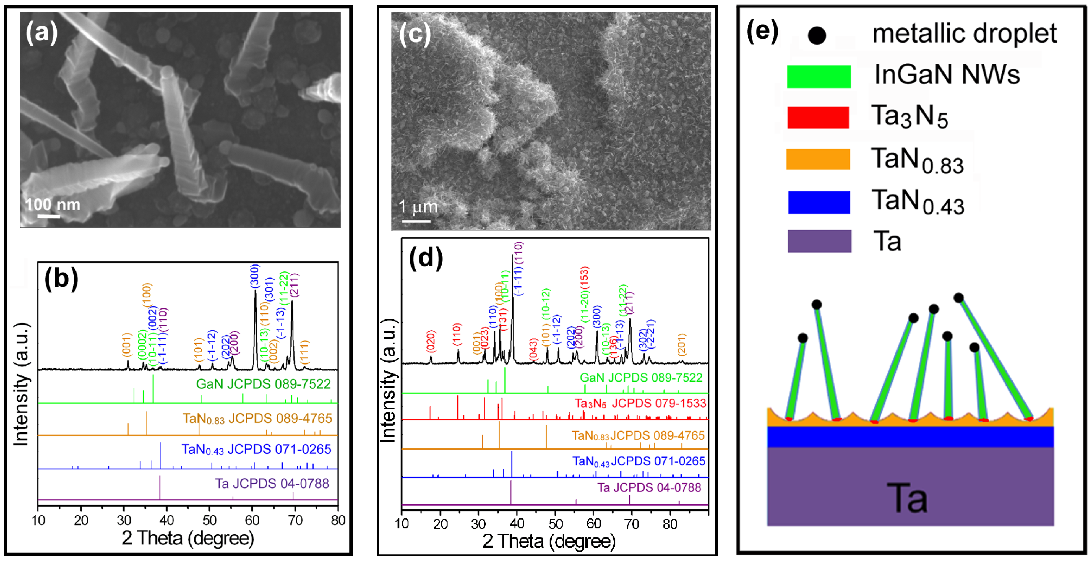
3.1. CVD Growth on the Native and Oxidative Ta Substrates

After the CVD growth, neither native nor oxidative Ta surfaces can lead to the growth of NWs. On the surface of the oxidative Ta substrates, only metallic clusters, polish scratches, and film cracks can be observed in the SEM images as shown by Figure 2a–c. XRD spectra in Figure 2d showed that a crystalline β-Ta2O5 phase formed on the Ta surface, whose peak intensities decreased with increasing substrate temperatures in the order of 700 °C, 725 °C, and 750 °C. The observation indicated that the volatile nature of the Ta2O5 films could be the reason why the NWs growth failed on the native and oxidative Ta substrates. The other possibility could be originated from the reductive reaction between the Ta2O5 film and the hydrogen and ammonia during the high temperature CVD growth.

3.2. CVD Growth on the Nitrided Ta Substrates

The above results indicated that rather than an oxidative Ta surface, a nitrided Ta surface is more likely to be a substrate for the CVD grown InxGa1−xN NWs. Nitridation of the thermally oxidative Ta substrates, however, resulted in a peeled film off the Ta substrate. As a consequence, electrochemical anodic oxidative Ta was used for the post-nitridation process. Short-time anodization of the Ta plates usually produced a thick sealed tubular oxide film with many cracks as shown by the inset of Figure 3a. On the top of the thick tubular oxide film existed a continuous passive film, which has been demonstrated to work as surface recombination centers of the electron-hole pairs and to deteriorate the device properties [28]. To solve these problems, a prolonged anodization process was used instead, which exfoliated the tubular film and exposed the underlying surface. The exposed surface contained a thin continuous oxide layer that exhibited a morphology of regular dimples ~250 nm in diameter (Figure 3a). After nitridation, the dimpled morphology was maintained and no cracks appeared on the surface (Figure 3b). XRD (Figure 3c) suggested the existence of Ta3N5, TaN0.83, and TaN0.43 on the nitrided Ta surface. The distributions of the phases were drawn schematically in Figure 3d, where it was proposed that the post-nitridation transformed the thin dimpled oxide layer into a thin dimpled Ta3N5 layer, with intermediate layers of TaN0.83 and TaN0.43 formed between the surface Ta3N5 layer and the Ta substrate.
After VLS-CVD growth, homogeneous distributions of long NWs were achieved only for the catalysts of Ni and Ni1Au1 (Figure 4a–e). SEM images also show that the more the content of Au, the less the density of NWs. The large particles distributed on the surface of the nitrided Ta substrates (Figure 4c–e) were revealed to be Au particles dissolved with a large amount of Ga and In (Figure 4f). It has been reported that Au atoms can detach and migrate along GaN nanowires grown on Si during the plasma-enhanced CVD process [29]. In our case, it seems that Au atoms were dewetting on the nitrided Ta surface and coalesced to form particles, whose sizes were too large to catalyze NWs growth.
For the catalyst of Ni1Au1, the obtained NWs had rough facets on the sidewalls and droplets on the top (Figure 5a). The later clearly indicated a VLS growth mechanism of the NWs. For the nitrided dimpled Ta surface with NWs, XRD spectrum in Figure 5b clearly revealed the presence of phases of GaN, TaN0.83, TaN0.43, and Ta, while the Ta3N5 phase was obviously missing. When a thick tubular Ta3N5 layer was used as the substrate (Figure 5c), the Ta3N5 phase remained in the XRD spectrum as shown by Figure 5d, indicating a stable Ta3N5 phase under a pressure of 2000 Pa at 800 °C. The absence of Ta3N5 peaks in Figure 5b could thereby be ascribed to the reduction of the thin dimpled Ta3N5 layer by hydrogen during the CVD growth. Although not detected by XRD, a small amount of Ta3N5 should still be present to bond the NWs and the TaN0.83 layer together, as shown schematically by Figure 5e. The survived Ta3N5 could be owing to the protection of the catalyst droplets. The stable Ta3N5 intermediate layer should be the main reason for the successful fabrication of nitride NWs on the Ta surface.

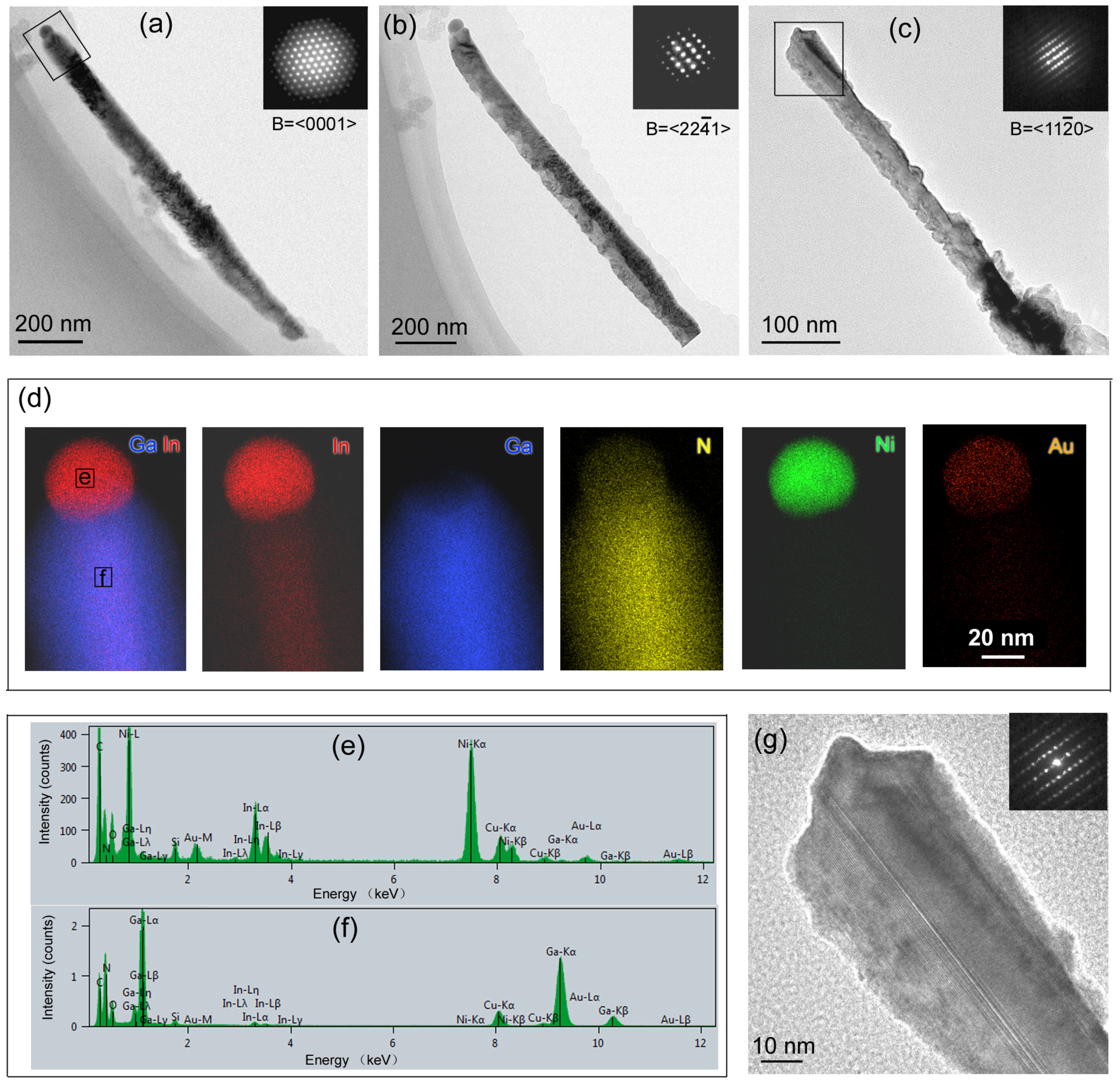
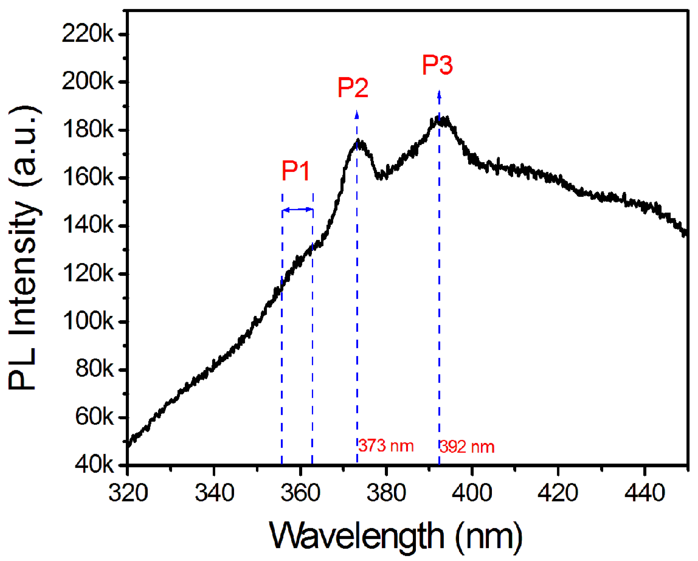
3.3. TEM Characterization of InxGa1−xN NWs on Nitrided Ta Substrates

TEM characterizations were performed on the NWs, which were removed from the Ta substrate by sonication in a methanol solution and collected by the copper grids with a carbon film. Bright-field (BF) TEM images showed that the diameter of the NWs ranges from 50 to 100 nm, and their length is on the order of microns. The converged beam electron diffraction (CBED) patterns viewed along three different directions all verified a wurtzite structure with a NW growth direction of [1100] (Figure 6a–c). According to the element mappings (Figure 6d) and the EDS spectra (Figure 6e,f), neither droplets nor NWs contained Ta atoms. Instead, the droplet consisted of nitrogen and three metallic elements with a relative concentration of 75.8 at.% Ni, 22.5 at.% In, and 1.7 at.% Au (Figure 6e). The ratio of Au in the droplet was much less than the original catalyst solution (Ni1Au1), which is consistent with the SEM observation that Au atoms tend to migrate on the nitrided Ta surface. EDS/STEM mapping in Figure 6d also revealed a core-shell structure for the NW with an InxGa1−xN core around 20–30 nm in diameter and a GaN-shell around 10–20 nm in thickness. Repeated EDS/STEM measurements were conducted on the core regions in different NWs and a typical EDS spectrum was shown in Figure 6f. Quantification results showed that the InxGa1−xN cores had “x” varying between 1.3 to 3.5 at.%. It should be noted that since the InxGa1−xN core was wrapped with a GaN shell, the obtained indium composition “x” is actually an average composition of the NW and could be lower than the true value of the core. High resolution TEM (HRTEM) of the NWs found no dislocations but showed the presence of the basal stacking faults (BSFs) inside the InxGa1−xN cores (Figure 6g).
Low-temperature (LT) PL was employed to characterize the NWs as shown by Figure 7. The sample showed a weak PL shoulder (P1) between 355–362 nm, which could correspond to the neutral donor bound A exciton (D0, XA) recombination (358 nm/3.472 eV) and free A exciton (XA) recombination (357.5 nm/3.477 eV) of the thin GaN shells in the NWs [14,15,30,31]. The second peak P2 is located at 373 nm, which can be attributed to the XA peak from InxGa1−xN core. Based on P2, the band gap energy of the InxGa1−xN cores in the NWs can be estimated as 3.32 eV. The average indium concentration x in the NW cores can be obtained by using equation Eg = 0.7x + 3.477(1 − x) − bx(1 − x), where Eg, 0.7, and 3.477 are the bandgap energy of InxGa1−xN, InN, and GaN, respectively, and b represents the bowing parameter [32]. The indium concentration x in the NW cores can therefore be calculated to be 2.4 at.% or 3.8 at.%, depending on the choice of bowing parameter b as 3.6 eV [33] or 1.4 eV [32]. The indium concentration calculated from P2 peak in PL matches quite well with those measured from EDS/STEM. The third peak P3 at 392 nm could arise from two reasons. The first one is the XA peak from InxGa1−xN with higher indium composition, which is vetoed since a thorough TEM examination has been carried out and neither NW nor quantum dots with high indium concentration can be found. Therefore, it is more likely to be true to associate the relatively broad P3 peak with the structural defects such as basal stacking fault in the InxGa1−xN core [14,15,30,31,34], which has been observed in the InxGa1−xN core as shown in Figure 6g.
To summarize, our investigation showed that tantalum oxide is not stable under the CVD growth conditions. Instead, tantalum nitrides were demonstrated to be more suited as a substrate for InxGa1−xN NWs. The nitrided dimpled Ta surface contained a thin continuous Ta3N5 layer, which can work as an intermediate layer to bond the InxGa1−xN NWs and the substrate. The underlying substrate contained TaN0.83, TaN0.43, and Ta, all of which are conductive. Therefore, in terms of the transport of the photo-generated carriers, Ta should be superior to the conventional Si substrate because of an insulated SixNy layer formed on the surface of Si [19]. On a dimpled surface of tantalum nitrides, Au atoms tend to coalesce rather than form nano-droplets to catalyze NW growth. Ni was proved to be the suitable catalyst for the VLS-CVD growth of InxGa1−xN NWs. The obtained core-shell structure for the NWs could be explained by an initial VLS-growth of the InxGa1−xN core and a subsequent VS-growth of the GaN shell, which will be investigated and discussed in the future. Although not affected by the Ta substrate, the composition of InxGa1−xN NWs should be further adjusted by changing the CVD growth parameters, such as temperature and pressure. Once higher indium content can be achieved in InxGa1−xN NWs, a matched energy band structure can be established between the InxGa1−xN NWs and the Ta3N5 surface layer. Furthermore, the BSFs in the m-InxGa1−xN NWs could also help to accelerate the separation of photogenerated hole-electron pairs in the devices such as solar cells and photo-detectors. Therefore, VLS-CVD fabrication of the InxGa1−xN NWs/Ta electrode holds great promise as a large-scale manufacture method for solar cells, photo-detectors, and photo-catalytic devices.

4. Conclusions

InxGa1−xN NWs were successfully grown on Ta substrates via VLS-CVD. A Ta surface pretreatment method was developed by a combination of electrochemical anodization and high temperature nitridation, leading to a dimpled Ta3N5 surface layer with underlying intermediate layers of TaN0.83 and TaN0.43. Ni rather than Au was demonstrated as the suitable catalyst for VLS-CVD growth of NWs on the Ta templates. The obtained InxGa1−xN NWs grew along a [1100] direction and processed an InxGa1−xN core/GaN shell structure with the presence of basal SFs in the InxGa1−xN core.

Author Contributions

Methodology and writing, Y.-L.H.; Investigation, Y.Z., H.J., Q.L., A.F., X.W., G.X., H.Y., J.L., J.S., D.S.; Review & Editing: D.W.

Funding

This work is supported by the National Natural Science Foundation of China (No. 51402249 and No. 51572191), the Natural Science Foundation of Fujian Province (No. 2017J01593), the Research Fund Programs for Returnees of Xiamen (No. 2016166), the Fundamental Research Funds for the Central Universities (No. 30916014103), Open fund of Fujian Provincial Key Laboratory of Functional Materials and Applications (Xiamen University of Technology), and the Program for Innovative Research Team in Science and Technology in Fujian Province University (IRTSTFJ).

Conflicts of Interest

The authors declare no conflict of interest.

References

  1. Nakamura, S.; Fasol, G. The Blue Laser Diode: GaN Based Light Emitters and Lasers; Springer: Berlin/Heidelberg, Germany, 1997; ISBN-10: 3540615903. [Google Scholar]
  2. Fujii, K.; Kusakabe, K.; Ohkawa, K. Photoelectrochemical Properties of InGaN for H2 Generation from Aqueous Water. Jpn. J. Appl. Phys. 2005, 44, 7433–7435. [Google Scholar] [CrossRef]
  3. AlOtaibi, B.; Fan, S.; Wang, D.; Ye, J.; Mi, Z. Wafer-Level Artificial Photosynthesis for CO2 Reduction into CH4 and CO Using GaN Nanowires. ACS Catal. 2015, 5, 5342–5348. [Google Scholar] [CrossRef]
  4. Wang, S.; Sun, C.; Shao, Y.; Wu, Y.; Zhang, L.; Hao, X. Self-Supporting GaN Nanowires/Graphite Paper: Novel High-Performance Flexible Supercapacitor Electrodes. Small 2017, 13, 1603330. [Google Scholar] [CrossRef] [PubMed]
  5. Wang, S.; Zhang, L.; Sun, C.; Shao, Y.; Wu, Y.; Lv, J.; Hao, X. Gallium Nitride Crystals: Novel Supercapacitor Electrode Materials. Adv. Mater. 2016, 28, 3768–3776. [Google Scholar] [CrossRef] [PubMed]
  6. Wang, D.; Pierre, A.; Kibria, M.G.; Cui, K.; Han, X.; Bevan, K.H.; Guo, H.; Paradis, S.; Hakima, A.-R.; Mi, Z. Wafer-Level Photocatalytic Water Splitting on GaN Nanowire Arrays Grown by Molecular Beam Epitaxy. Nano Lett. 2011, 11, 2353–2357. [Google Scholar] [CrossRef] [PubMed]
  7. Kuykendall, T.; Ulrich, P.; Aloni, S.; Yang, P. Complete Composition Tunability of InGaN Nanowires Using a Combinatorial Approach. Nat. Mater. 2007, 6, 951–956. [Google Scholar] [CrossRef] [PubMed]
  8. Kuykendall, T.R.; Schwartzberg, A.M.; Aloni, S. Gallium Nitride Nanowires and Heterostructures: Toward Color-Tunable and White-Light Sources. Adv. Mater. 2015, 27, 5805–5812. [Google Scholar] [CrossRef] [PubMed]
  9. Ra, Y.-H.; Wang, R.; Woo, S.Y.; Djavid, M.; Sadaf, S.Md.; Lee, J.; Botton, G.A.; Mi, Z. Full-Color Single Nanowire Pixels for Projection Displays. Nano Lett. 2016, 16, 4608–4615. [Google Scholar] [CrossRef] [PubMed]
  10. Fan, S.; Woo, S.Y.; Vanka, S.; Botton, G.A.; Mi, Z. An In0.5Ga0.5N Nanowire Photoanode for Harvesting Deep Visible Light Photons. APL Mater. 2016, 4, 076106. [Google Scholar] [CrossRef]
  11. Zhao, C.; Ng, T.K.; Wei, N.; Prabaswara, A.; Alias, M.S.; Janjua, B.; Shen, C.; Ooi, B.S. Facile Formation of High-Quality InGaN/GaN Quantum-Disks-in-Nanowires on Bulk-Metal Substrates for High-Power Light-Emitters. Nano Lett. 2016, 16, 1056–1063. [Google Scholar] [CrossRef] [PubMed]
  12. Wolz, M.; Hauswald, C.; Flissikowski, T.; Gotschke, T.; Fernandez-Garrido, S.; Brandt, O.; Grahn, H.T.; Geelhaar, L.; Riechert, H. Epitaxial Growth of GaN Nanowires with High Structural Perfection on a Metallic TiN Film. Nano Lett. 2015, 15, 3743–3747. [Google Scholar] [CrossRef] [PubMed]
  13. Sarwar, A.G.; Carnevale, S.D.; Yang, F.; Kent, T.F.; Jamison, J.J.; McComb, D.W.; Myers, R.C. Semiconductor Nanowire Light-Emitting Diodes Grown on Metal: A Direction Toward Large-Scale Fabrication of Nanowire Devices. Small 2015, 11, 5402–5408. [Google Scholar] [CrossRef] [PubMed]
  14. May, B.J.; Sarwar, A.T.M.G.; Myers, R.C. Nanowire LEDs Grown Directly on Flexible Metal Foil. Appl. Phys. Lett. 2016, 108, 141103. [Google Scholar] [CrossRef]
  15. Bae, S.-Y.; Lekhal, K.; Lee, H.-J.; Mitsunari, T.; Min, J.-W.; Lee, D.-S.; Kushimoto, M.; Honda, Y.; Amano, H. Selective-area Growth of Vertically Oriented GaN Nanostructures with a Hafnium Pre-orienting Layer. J. Cryst. Growth 2017, 468, 110–113. [Google Scholar] [CrossRef]
  16. Zhong, M.M.; Qin, F.W.; Liu, Y.M.; Wang, C.; Bian, J.M.; Wang, E.P.; Wang, H.; Zhang, D. Low-temperature Growth of High c-orientated Crystalline GaN Films on Amorphous Ni/glass Substrates with ECR-PEMOCVD. J. Alloy. Compd. 2014, 583, 39–42. [Google Scholar] [CrossRef]
  17. Li, H.; Zhao, G.; Wang, L.; Chen, Z.; Yang, S. Morphology Controlled Fabrication of InN Nanowires on Brass Substrates. Nanomaterials 2016, 6, 195. [Google Scholar] [CrossRef] [PubMed]
  18. Pendyala, C.; Jasinski, J.B.; Kim, J.H.; Vendra, V.K.; Lisenkov, S.; Menond, M.; Sunkara, M.K. Nanowires as Semi-rigid Substrates for Growth of Thick, InxGa1−xN (x > 0.4) Epi-layers without Phase Segregation for Photoelectrochemical Water Splitting. Nanoscale 2012, 4, 6269–6275. [Google Scholar] [CrossRef] [PubMed]
  19. Zhao, C.; Alfaraj, N.; Subedi, R.C.; Liang, J.W.; Alatawi, A.A.; Alhamoud, A.A.; Ebaid, M.; Alias, M.S.; Ng, T.K.; Ooi, B.S. III-nitride Nanowires on Unconventional Substrates: From Materials to Optoelectronic Device Applications. Progress Quantum Electron. 2018, 61, 1–31. [Google Scholar] [CrossRef]
  20. Chaneliere, C.; Autran, J.L.; Devine, R.A.B.; Balland, B. Tantalum Pentoxide (Ta2O5) Thin Films for Advanced Dielectric Application. Mater. Sci. Eng. R 1998, 22, 269–322. [Google Scholar] [CrossRef]
  21. Allam, N.K.; Feng, X.J.; Grimes, C.A. Self-Assembled Fabrication of Vertically Oriented Ta2O5 Nanotube Arrays, and Membranes Thereof, by One-Step Tantalum Anodization. Chem. Mater. 2008, 20, 6477–6481. [Google Scholar] [CrossRef]
  22. El-Sayed, H.A.; Molero, H.M.; Birss, V.I. The Impact of Fabrication Conditions on the Quality of Au Nanoparticle Arrays on Dimpled Ta Templates. Nanotechnology 2012, 23, 435602. [Google Scholar] [CrossRef] [PubMed]
  23. Dabirian, A.; Krol, R. High-Temperature Ammonolysis of Thin Film Ta2O5 Photoanodes: Evolution of Structural, Optical, and Photoelectrochemical Properties. Chem. Mater. 2015, 27, 708–715. [Google Scholar] [CrossRef]
  24. Hara, M.; Chiba, E.; Ishikawa, A.; Takata, T.; Kondo, J.N.; Domen, K. Ta3N5 and TaON Thin Films on Ta Foil: Surface Composition and Stability. J. Phys. Chem. B 2003, 107, 13441–13445. [Google Scholar] [CrossRef]
  25. Chun, W.-J.; Ishikawa, A.; Fujisawa, H.; Takata, T.; Kondo, J.N.; Hara, M.; Kawai, M.; Matsumoto, Y.; Domen, K. Conduction and Valence Band Positions of Ta2O5, TaON, and Ta3N5 by UPS and Electrochemical Methods. J. Phys. Chem. B 2003, 107, 1798–1803. [Google Scholar] [CrossRef]
  26. Wang, L.; Zhou, X.; Nguyen, N.T.; Hwang, I.; Schmuki, P. Strongly Enhanced Water Splitting Performance of Ta3N5 Nanotube Photoanodes with Subnitrides. Adv. Mater. 2016, 28, 2432–2438. [Google Scholar] [CrossRef] [PubMed]
  27. Chen, L.-Y.; Liao, C.-I.; Peng, H.-Y. Influence of Gas Flow Rates on the Formation of III-nitride Nanowires. Phys. Status Solidi C 2010, 7, 40–43. [Google Scholar] [CrossRef]
  28. Li, M.; Luo, W.; Cao, D.; Zhao, X.; Li, Z.; Yu, T.; Zou, Z. A Co-catalyst-Loaded Ta3N5 Photoanode with a High Solar Photocurrent for Water Splitting upon Facile Removal of the Surface Layer. Angew. Chem. Int. Ed. 2013, 52, 11016–11020. [Google Scholar] [CrossRef] [PubMed]
  29. Hou, W.-C.; Chen, L.-Y.; Tang, W.-C.; Hong, F.C.N. Control of Seed Detachment in Au-Assisted GaN Nanowire Growths. Cryst. Growth Des. 2011, 11, 990–994. [Google Scholar] [CrossRef]
  30. Calabrese, G.; Corfdir, P.; Gao, G.; Pfuller, C.; Trampert, A.; Brandt, O.; Geelhaar, L.; Fernández-Garrido, S. Molecular beam epitaxy of single crystalline GaN nanowires on a flexible Ti foil. Appl. Phys. Lett. 2016, 108, 202101. [Google Scholar] [CrossRef] [Green Version]
  31. Liu, R.; Bell, A.; Ponce, F.A.; Chen, C.Q.; Yang, J.W.; Khan, M.A. Luminescence from stacking faults in gallium nitride. Appl. Phys. Lett. 2005, 86, 021908. [Google Scholar] [CrossRef]
  32. Moses, P.G.; Van de Walle, C.G. Band Bowing and Band Alignment in InGaN Alloys. Appl. Phys. Lett. 2010, 96, 021908. [Google Scholar] [CrossRef]
  33. Aschenbrenner, T.; Figge, S.; Schowalter, M.; Rosenauer, A.; Hommel, D. Photoluminescence and Structural Analysis of a-plane InGaN Layers. J. Cryst. Growth 2008, 310, 4992–4995. [Google Scholar] [CrossRef]
  34. Fischer, A.M.; Wu, Z.; Sun, K.; Wei, Q.; Huang, Y.; Senda1, R.; Iida, D.; Iwaya, M.; Amano, H.; Ponce, F.A. Misfit Strain Relaxation by Stacking Fault Generation in InGaN Quantum Wells Grown on m-Plane GaN. Appl. Phys. Express 2009, 2, 041002. [Google Scholar] [CrossRef]
Figure 1. Schematic diagram of the CVD growth apparatus.
Nanomaterials 08 00990 g001
Figure 2. (ac) The top-view SEM images and (d) the corresponding XRD spectra of the oxidative Ta samples after CVD growth using a catalyst of Ni1Au1 with the substrate temperatures of (a) 700 °C, (b) 725 °C, and (c) 750 °C.
Nanomaterials 08 00990 g002
Figure 3. (a) The top-view SEM image of the Ta sample anodized at 80V for 10 min (with the inset showing the one anodized at 80V for 2 min). (b) The top-view SEM image and (c) XRD of the nitrided Ta sample. (d) Cross-sections schematic diagrams of the Ta surfaces.
Nanomaterials 08 00990 g003
Figure 4. Top-view SEM images of the InxGa1−xN NWs grown on the nitrided Ta surfaces using catalysts of (a) Ni, (b) Ni1Au1, (c) Ni1Au2, (d) Ni1Au4, and (e) Au. (f) The EDS spectrum (spectrum 1) from a large particle in the inset which is the top-view SEM image of a nitrided dimpled Ta surface after CVD growth using catalysts of Ni1Au4.
Nanomaterials 08 00990 g004
Figure 5. (a) The enlarged top-view SEM image and (b) XRD spectrum of the nitrided sample from a thin dimpled Ta surface; (c) the top-view SEM image and (d) XRD spectrum of the nitrided Ta sample with a thick tubular oxide film after CVD growth using catalysts of Ni1Au1. (e) The cross-section schematic diagram of the nitrided sample from a thin dimple Ta surface after the CVD growth.
Nanomaterials 08 00990 g005
Figure 6. (ac) BF TEM images and the corresponding CBED patterns (insets) of the InxGa1−xN NWs using the Ni1Au1 as a catalyst; (d) STEM/EDS element mappings of the region enclosed in Figure 4a; STEM/EDS spectra of the NW from the locations (e,f) in Figure 4d. (g) The HRTEM image and the corresponding SADP pattern viewed along [1120] for the region enclosed in Figure 4c.
Nanomaterials 08 00990 g006
Figure 7. PL measurement at 77 K of InxGa1−xN NWs on a pretreated Ta substrate using Ni as a catalyst.
Nanomaterials 08 00990 g007

