Exfoliation and Characterization of V2Se9 Atomic Crystals
by
 , and
, and
Bum Jun Kim
1,†, 
Byung Joo Jeong
2,†,
Seungbae OH
2,
Sudong Chae
2,
Kyung Hwan Choi
1,
Tuqeer Nasir
1,
Sang Hoon Lee
2,
Kwan-Woo Kim
2,
Hyung Kyu Lim
2,
Ik Jun Choi
2,
Ji-Yun Moon
3,
Hak Ki Yu
3,
Jae-Hyun Lee
3,* and
Jae-Young Choi
1,2,* 1
SKKU Advanced Institute of Nanotechnology, Sungkyunkwan University, Suwon 16419, Korea
2
School of Advanced Materials Science and Engineering, Sungkyunkwan University, Suwon 16419, Korea
3
Department of Materials Science and Engineering and Department of Energy Systems Research, Ajou University, Suwon 16499, Korea
*
Authors to whom correspondence should be addressed.
†
These authors contributed equally to this work.
Nanomaterials 2018, 8(9), 737; https://doi.org/10.3390/nano8090737
Submission received: 31 August 2018
/
Revised: 12 September 2018
/
Accepted: 18 September 2018
/
Published: 18 September 2018
(This article belongs to the Special Issue Preparation and Properties of 2D Materials)
Abstract
:Mass production of one-dimensional, V2Se9 crystals, was successfully synthesized using the solid-state reaction of vanadium and selenium. Through the mechanical exfoliation method, the bulk V2Se9 crystal was easily separated to nanoribbon structure and we have confirmed that as-grown V2Se9 crystals consist of innumerable single V2Se9 chains linked by van der Waals interaction. The exfoliated V2Se9 flakes can be controlled thickness by the repeated-peeling method. In addition, atomic thick nanoribbon structure of V2Se9 was also obtained on a 300 nm SiO2/Si substrate. Scanning Kelvin probe microscopy analysis was used to explore the variation of work function depending on the thickness of V2Se9 flakes. We believe that these observations will be of great help in selecting suitable metal contacts for V2Se9 and that a V2Se9 crystal is expected to have an important role in future nano-electronic devices.
1. Introduction
To overcome the high-density integration of electronic technology, which faces physical limitations (e.g., fabrication process and reduction in charge carrier mobility), researchers have been intensively trying to develop a new device architecture or novel materials [1,2,3,4]. A range of diverse candidate materials have been proposed since the 2000s. Among them, graphene, which is a single layer of carbon atoms arranged in a hexagonal lattice, is considered to be a promising solution for future electronic devices because of its superior physical properties such as high carrier mobility and excellent chemical stability; however, it has the fatal disadvantage in that it has difficulty forming a band gap [1,2,5,6,7]. Therefore, the development of applications for graphene-based electronic devices, the most promising field, does not meet public’ expectation yet. Graphene nanoribbons (GNRs) are presented as the effective way to open the bandgap of graphene but it is difficult to produce a uniform width in large area [6,7]. In addition, the transport behavior of GNRs and newly introduced two-dimensional (2D) materials (e.g., transition metal dichalcogenides (TMDCs) and black phosphorous), with appropriate bandgaps, are reduced dramatically because of dangling bonds at the side edges and domain boundaries [8,9,10,11]. Unfortunately, most of the studies of the 2D material-based electronic devices thus far contain an etching process to define the conducting channel. Thus, the discovery of one-dimensional (1D) nanomaterials, which are free from edge and grain boundary scattering, is a key solution in the development of nano-electronic device.
Carbon nanotubes (CNTs), which exhibit high carrier mobility, ultimate mechanical strength, and chemical stability, have been considered as representative building blocks for next-generation transistors, chemical sensors, and nanocomposites [12,13,14]. However, the wide range of electronic structures that arise from the different chirality of the CNTs curtails the reliability of the manufacturing process of the nano-electronic devices [15]. Therefore, separation of single-chirality CNTs from the bulk CNTs or control of the chirality during the growth of the CNTs is required. Recently, studies on the synthesis and application of a new family of 1D nanomaterials in the form of three-dimensional (3D) bundles of numerous single-molecular chains coupled by weak van der Waals interactions have been reported [16,17,18,19,20,21]. For example, extensive studies on bulk synthesis and atomic-scale dispersion of the bio-compatible Mo6S9−xIx have been reported [21,22,23]. In addition, Sb2S3 was developed as an optoelectronic device by effectively reducing exciton decay due to the absence of dangling bonds [24]. Moreover, VS4 was utilized for an electrochemical energy storage device by using the van der Waals gap between the chains [25,26]. However, in the majority of studies on these materials, they have been utilized only as a thin-film structure, although the benefits of the layered characteristics can be exploited. In addition, the crystal structure of Mo6S9−xIx is not well defined because the position of the sulfur and iodine atoms bridged to the molybdenum atoms may vary even for the same stoichiometric composition.
In this study, we succeeded in mass producing 1D semiconductor V2Se9 crystals via a simple transport method. Through the mechanical exfoliation method, we confirmed that as-grown V2Se9 crystals consist of innumerable single V2Se9 chains linked via the van der Waals interaction, like graphite. In addition, a nanoribbons structure of V2Se9 which is capable of thickness control was obtained through repetitive mechanical exfoliation of the V2Se9 crystals. Lastly, the change in work function according to the thickness change of the V2Se9 flakes was analyzed by scanning Kelvin probe microscopy (SKPM) measurement.
2. Materials and Methods
Synthesis: V2Se9 was synthesized using V (Powder, −325 mesh, 99.5%, Sigma-Aldrich, St. Louis, MO, USA) and Se (powder, 99+%, Alfa Aesar, Haverhill, MA, USA). The mixture of V (0.2038 g) and Se (1.4213 or 1.9898 g) with a V to Se ratio of 2:9 or 2:12.6 was pelletized and then sealed in a 10 cm-long evacuated quartz tube. The quartz ampoule was heated for 120 h at a temperature of 300–400 °C (at 5.5 °C/h) and then cooled (at 10 °C/h). The resulting material was a dark gray sintered powder. The unreacted Se was sublimated by heat treatment in a tube furnace at 250 °C under Ar atmosphere for 24 h.
Mechanical exfoliation: The bulk V2Se9 was placed on wafer dicing tape (BT150EKL, Nitto Denko, Umeda, Osaka, Japan) and the materials were stuck several times to yield thinner-than-bulk materials. A substrate (300 nm SiO2/Si or bare Si) was cleaned by ultrasonication in acetone, ethanol, and DI water for 15 min, followed by heating at 100 °C in order to remove the moisture from the substrate. The polymer tape was adhered strongly to and pressed against the substrate. After adhesion, the polymer tape was removed from the substrate; this process was repeated for exfoliation.
Characterization: Powder X-ray diffraction (Mac Science, M18XHF22, Tokyo, Japan) was performed using Cu-Kα radiation (λ = 0.154 nm). Field emission-scanning electron microscopy (FE-SEM, Hitachi, S4300SE, Chiyoda, Tokyo, Japan) was operated at an acceleration voltage of 15 kV. Atomic force microscopy (AFM, Park systems, NX 10, Suwon, South Korea) was performed in a non-contact mode for the topographic analysis of the mechanically exfoliated V2Se9 on 300 nm Si/SiO2. The surface potentials of V2Se9 on Si substrate were measured by SKPM (Park systems, NX10, Suwon, South Korea) measurement using Si tips coated with Cr-Pt (Multi75-G, Budget Sensors Inc., 1113 Sofia, Bulgaria) with resonance frequencies of 75 kHz, a scan rate of 0.3 Hz, and sample bias of ±1 V.
3. Results and Discussion
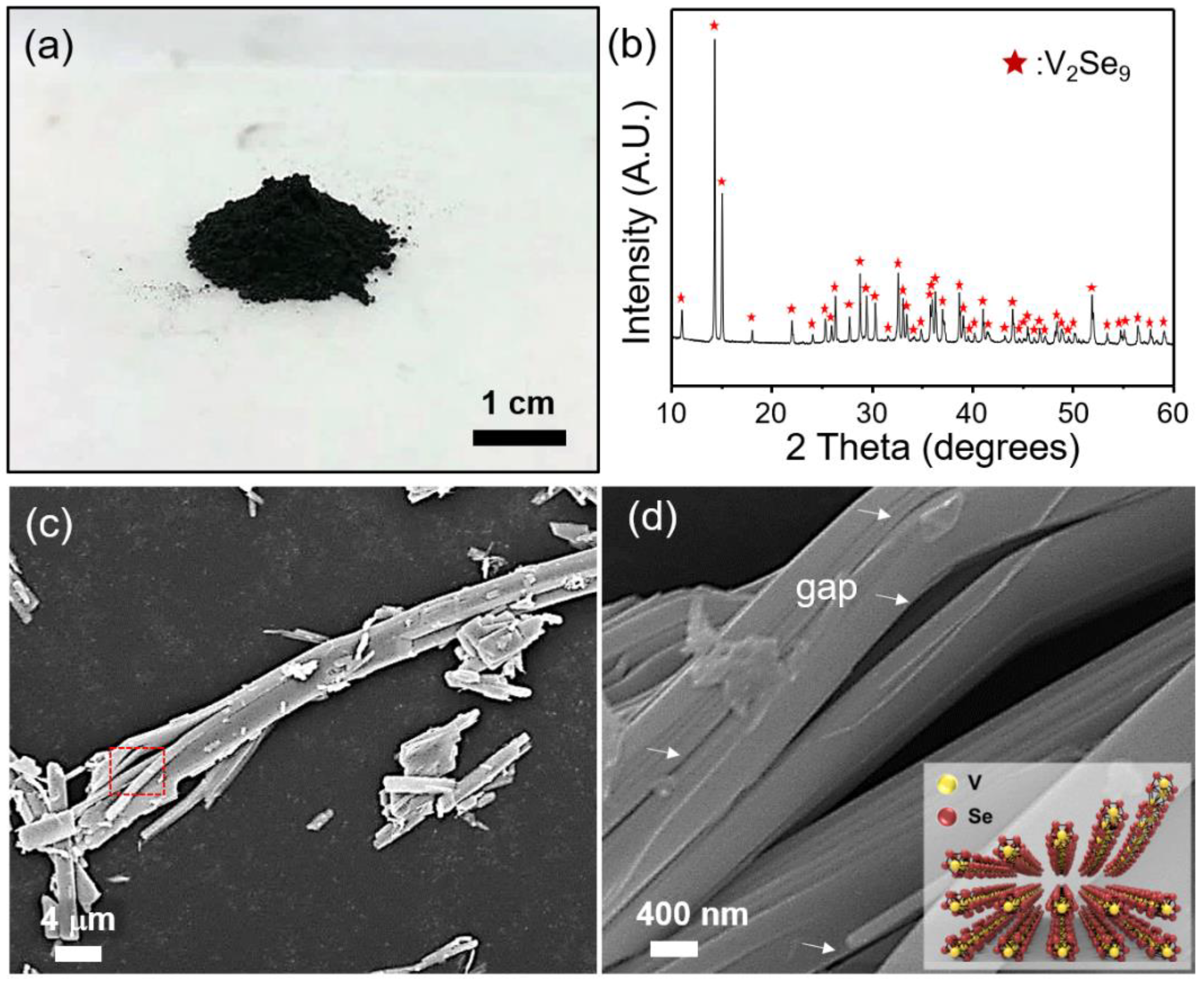
Since the transition metal vanadium has the outermost 3d orbital, it can produce various forms of compounds (e.g., V5Se4 to V2Se9) through a chemical reaction with selenium (see the phase diagram in Figure S1). Therefore, to synthesize V2Se9 crystals with a high-purity and high-crystallinity, the ratio of V:Se and the synthesis temperature should be considered carefully. For example, if the atomic mixing ratio of V and Se powder is adjusted precisely to 2:9 to synthesize V2Se9 crystals, unpredictable fluctuation occurs in the synthetic tube and VSe2, which is an undesirable impurity, is formed. We corrected these parameters experimentally, and as a result obtained pure V2Se9 crystals with an exact stoichiometry ratio of 2:9 by adding them in excess of Se, as shown in Figure 1a (V:Se atomic mixing ratio of 2:12.6). The crystallinity of the bulk V2Se9 crystal was verified by the X-ray diffraction (XRD) pattern (JCPDS 01-077-1589) (Figure 1b). The SEM images in Figure 1c,d clearly shows the 1D nanowire structures and the gaps generated during transfer of the sample onto the Si substrate.
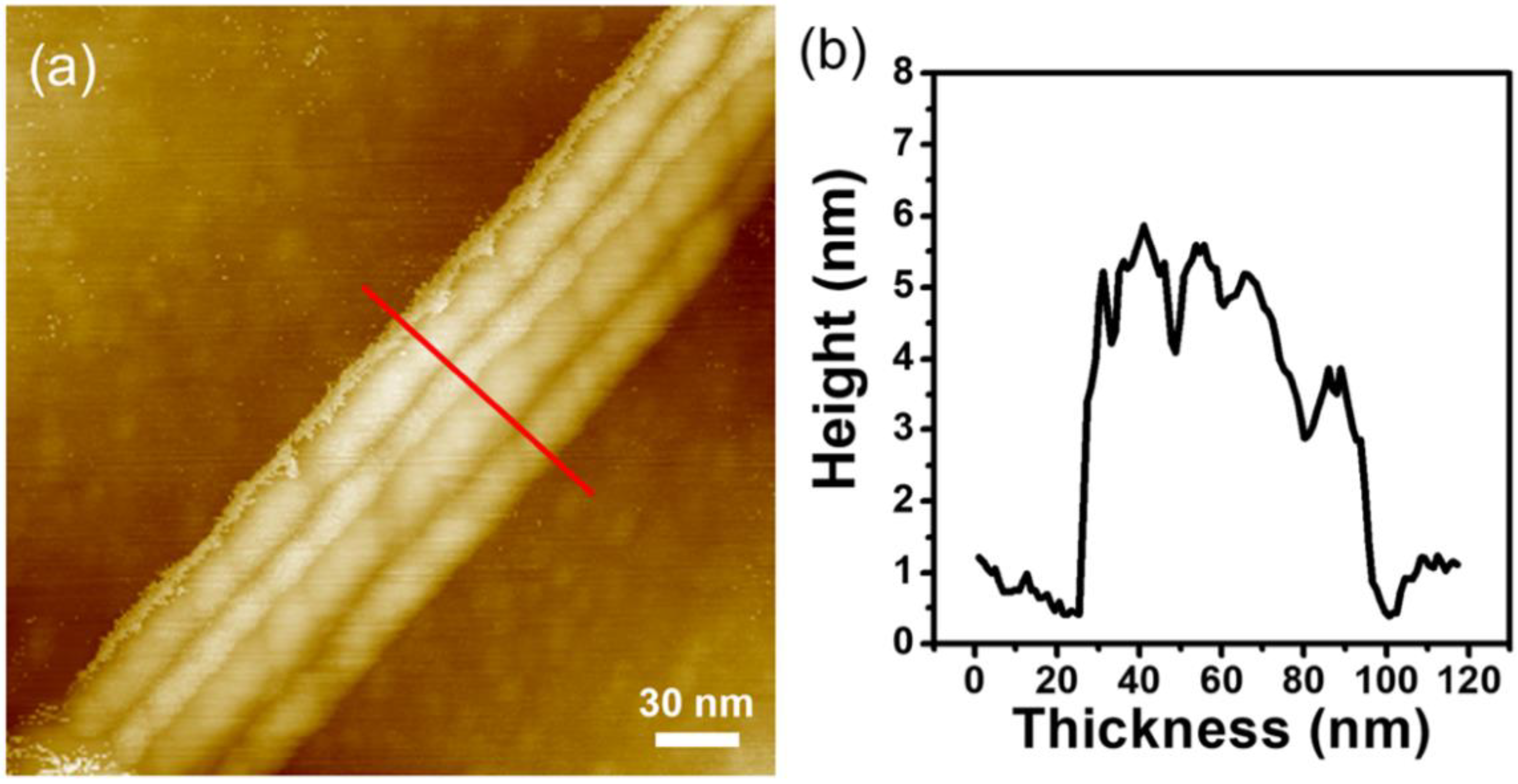
To investigate the structural characteristics of nanoscale V2Se9, the bulk V2Se9 crystal was mechanically exfoliated using the well-known tape method [1]. Although each single V2Se9 chains are linked by weak van der Waals interaction, we obtained a thin V2Se9 nanoribbon on a 300 nm SiO2/Si substrate (see in Figure 2). Unlike typical 2D materials, an exfoliated V2Se9 nanoribbon shows a rough surface.
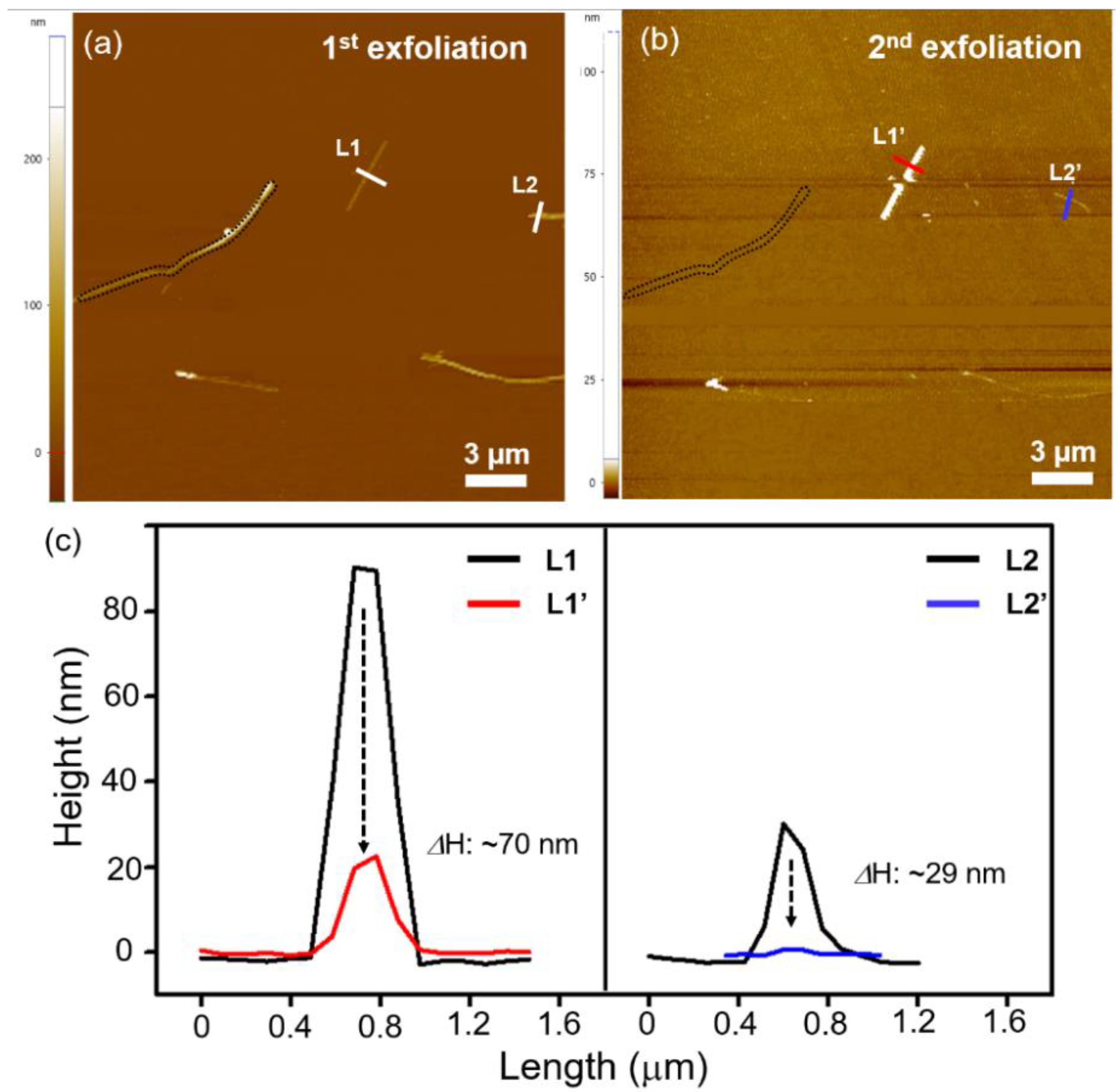
We attempted a further delamination at the sample position using the tape, and found that some of them had been torn out (black dotted line) and that the thickness decreased from 90 to 20 nm (L1 to L1′), and from 31 to 2 nm (L2 to L2′) (see Figure 3).
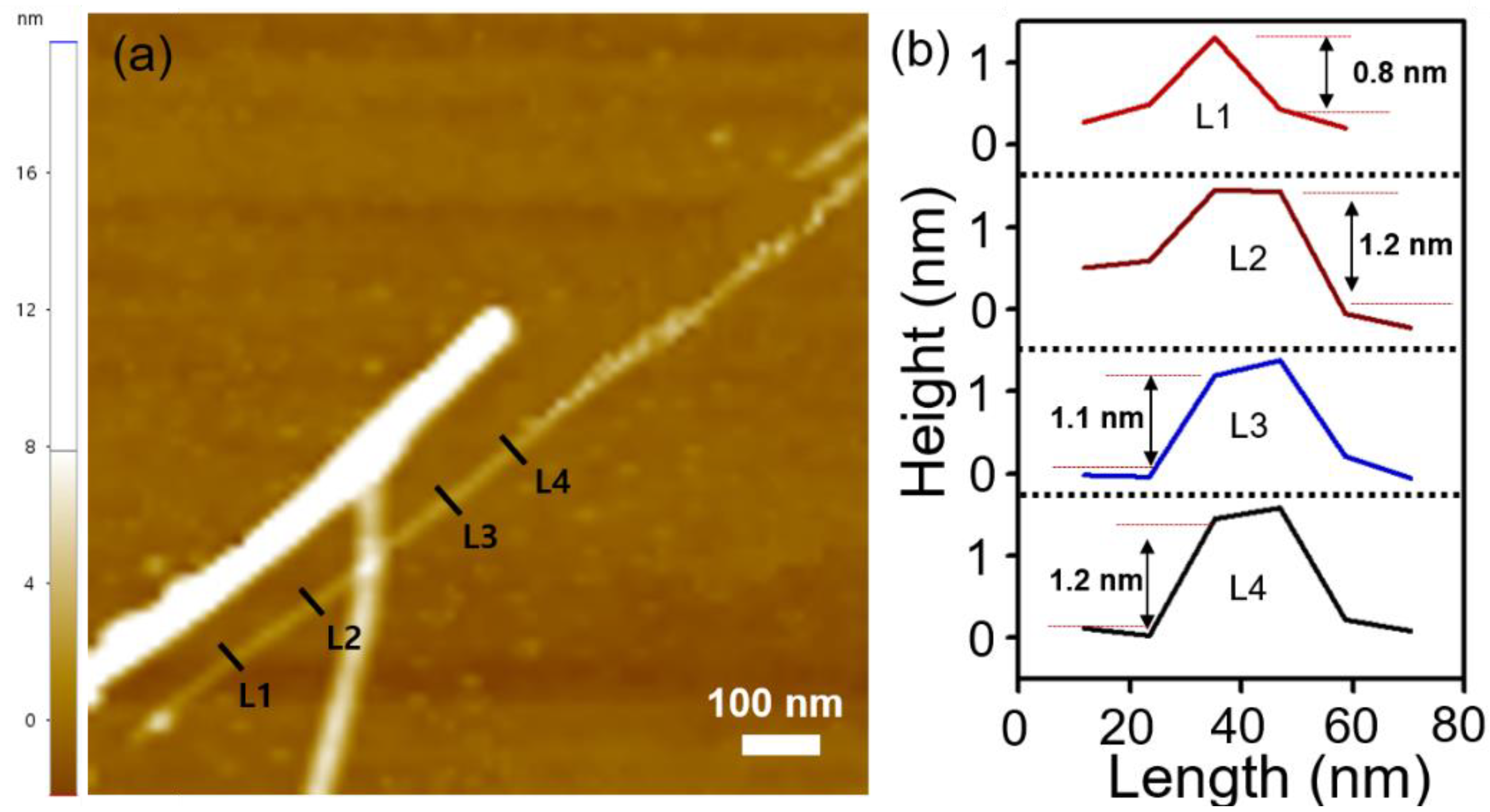
Figure 4a shows the AFM image of an isolated V2Se9 nanoribbon on the 300 nm SiO2/Si substrate. The nanoribbon has an atomic scale thickness and a width of approximately 20 nm (Figure 4b). Since V2Se9 has a bundle structure in which single chains are bonded by van der Waals forces, we expect that V2Se9 nanoribbons may exhibit ideal transport characteristics without degradation due to edge scattering.
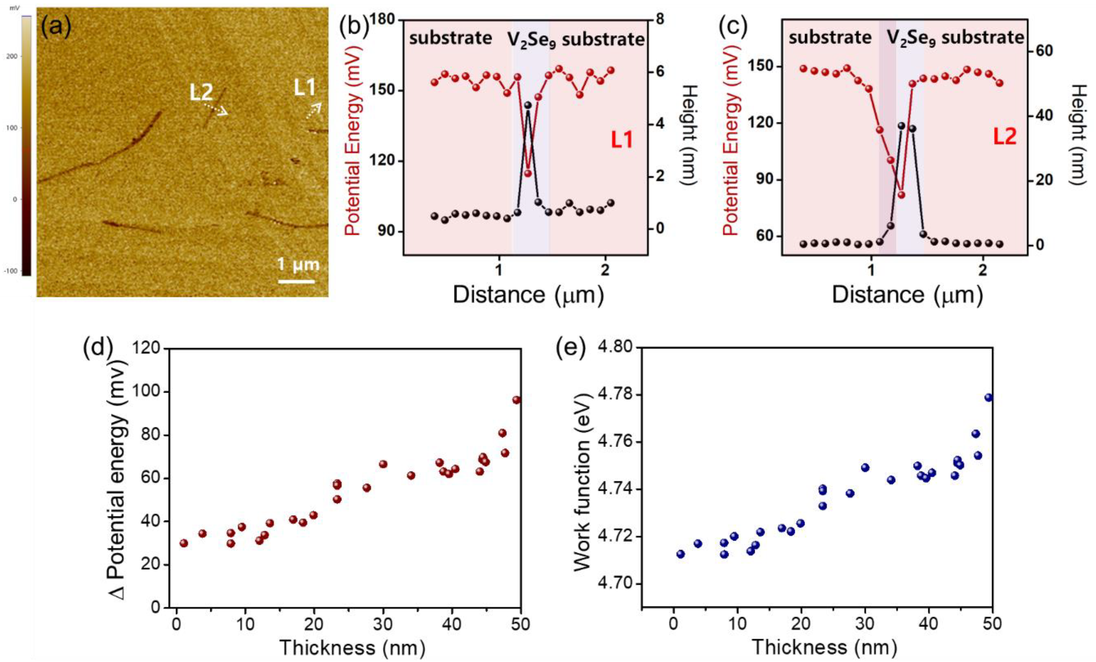
To investigate the electrical properties of V2Se9 flakes with a different number of layers, we performed an SKPM analysis, which is a non-destructive analytical tool that can investigate the local surface potential energy and work function by measuring the contact potential difference between the tip and the sample (VCPD) [27,28]. Because the V2Se9 nanoribbons were on the bare Si substrate, the work function of V2Se9 flakes can be calculated using the following equation:
where φt, φs and φf represent the work functions of the tip, Si substrate, and V2Se9 flake, respectively.
As shown in Figure 5a, the surface potential energy varies with the thickness of the V2Se9 flakes. For example, the surface potential energy differences (Δ potential energy) between the V2Se9 flakes with thicknesses of 5 and 40 nm and the Si substrate were 38 and 60 mV, respectively (Figure 5b,c). A Statistical analysis of more than 27 samples shows that as the thickness of the V2Se9 flake is less than 25 nm, the surface potential energy difference and the work function become to decrease simultaneously (Figure 5d,e). These phenomena can be explained using an interlayer screening effect, which is also observed in typical 2D materials [27,28,29]. In general, the native Si oxide (e.g., SiOx), which forms naturally on the surface of the Si wafer, has a hydrophilic property, which caused a large number of charge-trapping sites owing to the moisture in the air. Therefore, it affected the charge transfer between the V2Se9 flakes and the Si substrate [27]. Since the effective area of the interlayer screening effects increases with decreasing flake thickness, the surface potential difference and the work function of 25 nm thick V2Se9 flakes decreased from that of the bulk V2Se9 (See in Figure S2).
4. Conclusions
In conclusion, the mass production of the high-purity and high-crystalline 1D material V2Se9 crystals was successfully demonstrated using the solid-state reaction of V and Se. Through the mechanical exfoliation method, we confirmed that as-grown V2Se9 crystals consist of innumerable covalently bonded V2Se9 chains linked by the van der Waals interaction. In addition, atomic nanoribbons structures of V2Se9 was obtained on the 300 nm SiO2/Si substrate. We used SKPM analysis to investigate the electrical characteristics of V2Se9 and established that the work function decreased with decreasing thickness of the V2Se9 flakes owing to the interlayer screening effect. These results will be of great help in selecting suitable metal contacts for V2Se9; these will have a significant influence on the overall performance. We believe that the 1D semiconductor V2Se9 crystal is expected to be a new family of 2D materials that will be considered essential in future device applications.
Supplementary Materials
The following are available online at https://www.mdpi.com/2079-4991/8/9/737/s1, Figure S1: Phase diagram of V-Se binary system, Figure S2: SKPM image of exfoliated 1D V2Se9 flake.
Author Contributions
J.-Y.C. designed the experiments, and B.J.K. and B.J.J. supported the elemental analysis. S.O. and S.C. performed the chemical reaction experiments and K.H.C., T.N. and S.H.L. support the chemical reaction experiment and K.-W.K., H.K.L., I.J.C. and J.-Y.M. supported structural analysis. H.K.Y., J.-H.L. and J.-Y.C. conceived and supervised this study and provided intellectual and technical guidance.
Funding
This work was supported by the Technology Innovation Program (or Industrial Strategic Technology Development Program) (10063400, Development of Growth and Transfer Technology for Defectless 350 × 350 mm2 Single Crystalline Graphene) funded By the Ministry of Trade, Industry and Energy (MOTIE, Korea). J.H.L. acknowledges support from the Presidential Postdoctoral Fellowship Program of the National Research Foundation in Korea (2014R1A6A3A04058169).
Conflicts of Interest
The authors declare no conflict of interest.
References
- Novoselov, K.S.; Geim, A.K.; Morozov, S.V.; Jiang, D.; Katsnelson, M.I.; Grigorieva, I.V.; Dubonos, S.V.; Firsov, A. Two-dimensional gas of massless Dirac fermions in graphene. Nature 2005, 438, 197–200. [Google Scholar] [CrossRef] [PubMed] [Green Version]
- Zhang, Y.; Tan, Y.-W.; Stormer, H.L.; Kim, P. Experimental observation of the quantum Hall effect and Berry’s phase in graphene. Nature 2005, 438, 201–204. [Google Scholar] [CrossRef] [PubMed]
- Yang, H.; Heo, J.; Park, S.; Song, H.J.; Seo, D.H.; Byun, K.E.; Kim, P.; Yoo, I.; Chung, H.J.; Kim, K. Graphene barristor, a triode device with a gate-controlled Schottky barrier. Science 2012, 336, 1140–1143. [Google Scholar] [CrossRef] [PubMed]
- Geim, A.K.; Grigorieva, I.V. Van der Waals heterostructures. Nature 2013, 499, 419–425. [Google Scholar] [CrossRef] [PubMed] [Green Version]
- Lee, C.; Wei, X.; Kysar, J.W.; Hone, J. Measurement of the elastic properties and intrinsic strength of monolayer graphene. Science 2008, 321, 385–388. [Google Scholar] [CrossRef] [PubMed]
- Son, Y.W.; Cohen, M.L.; Louie, S.G. Half-metallic graphene nanoribbons. Nature 2006, 444, 347–349. [Google Scholar] [CrossRef] [PubMed] [Green Version]
- Avouris, P.; Chen, Z.; Perebeinos, V. Carbon-based electronics. Nat. Nanotechnol. 2007, 2, 605–615. [Google Scholar] [CrossRef] [PubMed]
- Radisavljevic, B.; Radenovic, A.; Brivio, J.; Giacometti, I.V.; Kis, A. Single-layer MoS2 transistors. Nat. Nanotechnol. 2011, 6, 147–150. [Google Scholar] [CrossRef] [PubMed]
- Qiao, J.; Kong, X.; Hu, Z.X.; Yang, F.; Ji, W. High-mobility transport anisotropy and linear dichroism in few-layer black phosphorus. Nat. Commun. 2014, 5, 4474. [Google Scholar] [CrossRef] [PubMed]
- Mayorov, A.S.; Gorbachev, R.V.; Morozov, S.V.; Britnell, L.; Jalil, R.; Ponomarenko, L.A.; Blake, P.; Novoselov, K.S.; Watanabe, K.; Taniguchi, T.; et al. Micrometer-scale ballistic transport in encapsulated graphene at room temperature. Nano Lett. 2011, 11, 2396–2399. [Google Scholar] [CrossRef] [PubMed]
- Schwierz, F. Graphene transistors. Nat. Nanotechnol. 2010, 5, 487–496. [Google Scholar] [CrossRef] [PubMed]
- Avouris, P.; Freitag, M.; Perebeinos, V. Carbon-nanotube photonics and optoelectronics. Nat. Photonics 2008, 2, 341–350. [Google Scholar] [CrossRef]
- Wang, J.; Musameh, M. Carbon nanotube/teflon composite electrochemical sensors and biosensors. Anal. Chem. 2003, 75, 2075–2079. [Google Scholar] [CrossRef] [PubMed]
- Chen, Z.; Augustyn, V.; Wen, J.; Zhang, Y.; Shen, M.; Dunn, B.; Lu, Y. High-performance supercapacitors based on intertwined CNT/V2O5 nanowire nanocomposites. Adv. Mater. 2011, 23, 791–795. [Google Scholar] [CrossRef] [PubMed]
- Kusunoki, M.; Suzuki, T.; Honjo, C.; Hirayama, T.; Shibata, N. Selective synthesis of zigzag-type aligned carbon nanotubes on SiC (0 0 0–1) wafers. Chem. Phys. Lett. 2002, 366, 458–462. [Google Scholar] [CrossRef]
- McCarthy, D.N.; Nicolosi, V.; Vengust, D.; Mihailovic, D.; Compagnini, G.; Blau, W.J.; Coleman, J.N. Dispersion and purification of Mo6S3I6 nanowires in organic solvents. J. Appl. Phys. 2007, 101, 014317. [Google Scholar] [CrossRef]
- Golden, J.H.; DiSalvo, F.J.; Fréchet, J.M.J.; Silcox, J.; Thomas, M.; Elman, J. Subnanometer-diameter wires isolated in a polymer matrix by fast polymerization. Science 1996, 273, 782–784. [Google Scholar] [CrossRef] [PubMed]
- Messer, B.; Song, J.H.; Huang, M.; Wu, Y.; Kim, F.; Yang, P. Surfactant-induced mesoscopic assemblies of inorganic molecular chains. Adv. Mater. 2000, 12, 1526–1528. [Google Scholar] [CrossRef]
- Heidelberg, A.; Bloeß, H.; Schultze, J.W.; Booth, C.J.; Samulski, E.T.; Boland, J.J. Electronic properties of LiMo3Se3 nanowires and Mo3Se3 nanowire-networks for nanoscale electronic devices. Z. Phys. Chem. 2003, 217, 573–585. [Google Scholar] [CrossRef]
- Osterloh, F.E.; Hiramatsu, H.; Dumas, R.K.; Liu, K. Fe3O4LiMo3Se3 nanoparticle clusters as superparamagnetic nanocompasses. Langmuir 2005, 21, 9709–9713. [Google Scholar] [CrossRef] [PubMed]
- Meden, A.; Kodre, A.; Gomilšek, J.P.; Arčon, I.; Vilfan, I.; Vrbanic, D.; Mrzel, A.; Mihailovic, D. Atomic and electronic structure of Mo6S9−xIx nanowires. Nanotechnology 2005, 16, 1578–1583. [Google Scholar] [CrossRef]
- Ploscaru, M.I.; Kokalj, S.J.; Uplaznik, M.; Vengust, D.; Turk, D.; Mrzel, A.; Mihailovic, D. Mo6S9−xIx nanowire recognitive molecular-scale connectivity. Nano Lett. 2007, 7, 1445–1448. [Google Scholar] [CrossRef] [PubMed]
- Sun, N.; McMullan, M.; Papakonstantinou, P.; Gao, H.; Zhang, X.; Mihailovic, D.; Li, M. Bioassembled nanocircuits of Mo6S9−xIx nanowires for electrochemical immunodetection of estrone hapten. Anal. Chem. 2008, 80, 3593–3597. [Google Scholar] [CrossRef] [PubMed]
- Zhou, Y.; Wang, L.; Chen, S.; Qin, S.; Liu, X.; Chen, J.; Xue, D.J.; Luo, M.; Cao, Y.; Cheng, Y.; et al. Thin-film Sb2Se3 photovoltaics with oriented one-dimensional ribbons and benign grain boundaries. Nat. Photonics 2015, 9, 409–415. [Google Scholar] [CrossRef]
- Xu, X.; Jeong, S.; Rout, C.S.; Oh, P.; Ko, M.; Kim, H.; Kim, M.G.; Cao, R.; Shin, H.S.; Cho, J. Lithium reaction mechanism and high rate capability of VS4 graphene nanocomposite as an anode material for lithium batteries. J. Mater. Chem. A 2014, 2, 10847–10853. [Google Scholar] [CrossRef]
- Britto, S.; Leskes, M.; Hua, X.; Hébert, C.A.; Shin, H.S.; Clarke, S.; Borkiewicz, O.; Chapman, K.W.; Seshadri, R.; Cho, J.; et al. Multiple Redox Modes in the Reversible Lithiation of High-Capacity, Peierls-Distorted Vanadium Sulfide. J. Am. Chem. Soc. 2015, 137, 8499–8508. [Google Scholar] [CrossRef] [PubMed] [Green Version]
- Lee, N.J.; Yoo, J.W.; Choi, Y.J.; Kang, C.J.; Jeon, D.Y.; Kim, D.C.; Seo, S.; Chung, H.J. The interlayer screening effect of graphene sheets investigated by Kelvin probe force microscopy. Appl. Phys. Lett. 2009, 95, 222107. [Google Scholar] [CrossRef]
- Choi, S.H.; Shaolin, Z.; Yang, W. Layer-number-dependent work function of MoS2 nanoflakes. J. Korean Phys. Soc. 2014, 64, 1550–1555. [Google Scholar] [CrossRef]
- Li, Y.; Xu, C.-Y.; Zhen, L. Surface potential and interlayer screening effects of few-layer MoS2 nanoflakes. Appl. Phys. Lett. 2013, 102, 143110. [Google Scholar] [CrossRef]
Figure 1.
(a) Photo-image of mass production of V2Se9 crystal. (b) XRD pattern of V2Se9 crystal. (c) Low- and (d) high-magnification SEM images of V2Se9 crystal. The inset shows an illustration of the crystal structure of V2Se9.
Figure 1.
(a) Photo-image of mass production of V2Se9 crystal. (b) XRD pattern of V2Se9 crystal. (c) Low- and (d) high-magnification SEM images of V2Se9 crystal. The inset shows an illustration of the crystal structure of V2Se9.

Figure 2.
(a) Atomic force microscopy (AFM) image of the 1D V2Se9 flake on 300 nm SiO2/Si substrate. (b) Line-profile of a V2Se9 flake as marked in Figure 2a.
Figure 2.
(a) Atomic force microscopy (AFM) image of the 1D V2Se9 flake on 300 nm SiO2/Si substrate. (b) Line-profile of a V2Se9 flake as marked in Figure 2a.

Figure 3.
(a) AFM image of exfoliated V2Se9 on 300 nm SiO2/Si substrate. (b) AFM image of additionally exfoliated V2Se9 on 300 nm SiO2/Si substrate. (c) Line-profile of 1D V2Se9 flakes on 300 nm SiO2/Si substrate before and after 2nd exfoliation.
Figure 3.
(a) AFM image of exfoliated V2Se9 on 300 nm SiO2/Si substrate. (b) AFM image of additionally exfoliated V2Se9 on 300 nm SiO2/Si substrate. (c) Line-profile of 1D V2Se9 flakes on 300 nm SiO2/Si substrate before and after 2nd exfoliation.

Figure 4.
(a) AFM image of the V2Se9 nanoribbon on the 300 nm SiO2/Si substrate. The inset shows an illustration of the V2Se9 nanoribbon. (b) Line-profiles of the V2Se9 nanoribbon as marked L1, L2, L3, and L4 in Figure 4a.
Figure 4.
(a) AFM image of the V2Se9 nanoribbon on the 300 nm SiO2/Si substrate. The inset shows an illustration of the V2Se9 nanoribbon. (b) Line-profiles of the V2Se9 nanoribbon as marked L1, L2, L3, and L4 in Figure 4a.

Figure 5.
(a) Scanning Kelvin probe microscopy (SKPM) image of exfoliated 1D V2Se9 flakes on the Si substrate. (b,c) Height and potential energy profiles of the V2Se9 flakes and Si substrate as labeled in Figure 5a. (d,e) Variation in potential energy difference and work function depending as a function of thickness of V2Se9 flakes.

© 2018 by the authors. Licensee MDPI, Basel, Switzerland. This article is an open access article distributed under the terms and conditions of the Creative Commons Attribution (CC BY) license (http://creativecommons.org/licenses/by/4.0/).
Share and Cite
MDPI and ACS Style
Kim, B.J.; Jeong, B.J.; OH, S.; Chae, S.; Choi, K.H.; Nasir, T.; Lee, S.H.; Kim, K.-W.; Lim, H.K.; Choi, I.J.; et al. Exfoliation and Characterization of V2Se9 Atomic Crystals. Nanomaterials 2018, 8, 737. https://doi.org/10.3390/nano8090737
AMA Style
Kim BJ, Jeong BJ, OH S, Chae S, Choi KH, Nasir T, Lee SH, Kim K-W, Lim HK, Choi IJ, et al. Exfoliation and Characterization of V2Se9 Atomic Crystals. Nanomaterials. 2018; 8(9):737. https://doi.org/10.3390/nano8090737
Chicago/Turabian StyleKim, Bum Jun, Byung Joo Jeong, Seungbae OH, Sudong Chae, Kyung Hwan Choi, Tuqeer Nasir, Sang Hoon Lee, Kwan-Woo Kim, Hyung Kyu Lim, Ik Jun Choi, and et al. 2018. "Exfoliation and Characterization of V2Se9 Atomic Crystals" Nanomaterials 8, no. 9: 737. https://doi.org/10.3390/nano8090737
Note that from the first issue of 2016, this journal uses article numbers instead of page numbers. See further details here.