Electrical Properties and Interfacial Issues of HfO2/Ge MIS Capacitors Characterized by the Thickness of La2O3 Interlayer


Key Laboratory for Wide Band Gap Semiconductor Materials and Devices of Education, School of Microelectronics, Xidian University, Xi’an 710071, China
*
Author to whom correspondence should be addressed.
Nanomaterials 2019, 9(5), 697; https://doi.org/10.3390/nano9050697
Submission received: 24 February 2019
/
Revised: 25 April 2019
/
Accepted: 29 April 2019
/
Published: 4 May 2019
(This article belongs to the Special Issue Design and Development of Nanostructured Thin Films)
Abstract
:Effects of the La2O3 passivation layer thickness on the interfacial properties of high-k/Ge interface are investigated systematically. In a very thin range (0~15 cycles), the increase of La2O3 passivation layer deposition cycles improves the surface smoothness of HfO2/Ge structures. The capacitance-voltage (C-V) characteristics show that the thickness of La2O3 passivation layer can affect the shift of flat band voltage (VFB), hysteretic behaviors, and the shapes of the dual-swept C-V curves. Moreover, significant improvements in the gate leakage current and breakdown characteristics are also achieved with the increase of La2O3 interlayer thickness.
1. Introduction
Along with the continuing scaling of complementary metal oxide semiconductor (CMOS) technology according to Moore’s Law, insulation oxides with higher permittivity have been introduced to replace SiO2 for acceptable gate leakage current density and low power consumption [1]. However, other than reducing feature size, technological progress to gain high-speed operation is also needed with the development of integrated circuit (IC) technology. Considering this, high mobility semiconductors have been considered as alternative channel materials for obtaining high drive current. Among the high mobility semiconductors, germanium (Ge) is compatible with standard Si CMOS process, and both the electron and hole bulk mobility are higher than those of Si substrate [2,3]. Therefore, Ge has been regarded as one of the most promising alternative channel materials. Unfortunately, different from the perfect interfacial properties of SiO2/Si interface, the poor thermal stability of GeO2/Ge interface results in the deterioration of interfacial properties to a great extent [4]. When most gate dielectric materials deposited on the unpassivated Ge substrate, the generation of unstable Ge oxides is unavoidable during the high temperature post-deposition annealing (PDA) process, and the decomposition or desorption from GeO2 to volatile GeO would bring in a great deal of defects. Consequently, to get acceptable electrical properties of high-k/Ge structures, a suitable surface passivation treatment is a necessary technical issue prior to the deposition of high-k gate dielectrics on Ge substrates [5].
Owing to the much better thermodynamic stability than that of GeO2/Ge, fewer interface traps exist at the interface between La-based oxides and Ge substrates [6]. Consequently, La-based oxides have been considered as one kind of the alternative gate dielectric materials deposited on Ge to realize good electrical performance of Ge-based metal-insulator-semiconductor (MIS) devices [7,8]. However, the hygroscopicity of La2O3 layer limits its application as gate insulators [9]. In a previous study, we have proved that a ~2 nm La2O3 interlayer could effectively improve the electrical performance of Ge MIS devices, resulting in more than one order of magnitude decrease in the gate leakage current density [10]. In this work, a further investigation was performed on the impacts of La2O3 passivation layer thickness on the interfacial properties of HfO2 insulators and Ge substrates.
2. Materials and Methods
La2O3 and HfO2 were deposited on Sb-doped n-type Ge (100) wafers with a doping concentration of 1 × 1016 cm−3 by atomic layer deposition (ALD) method (R-150, Picosun, Espoo, Finland). Prior to the deposition, all the wafers were treated using acetone and alcohol, followed by dipping into HF (2%) and deionized water by cyclic cleaning for 5 times to remove the defective native Ge oxide. Tris(isopropyl-cyclopentadienyl) lanthanum (La(i-PrCp)3) and tetrakis (ethylmethylamino) hafnium (TEMAH) were used as La and Hf precursor, while H2O was used as oxidant with reference to the reported literatures [11,12]. Under the chamber temperature of 300 °C, La2O3 layers were deposited by alternately introducing La(i-PrCp)3 and H2O precursors to the reactor chamber using high purity N2 (>99.999%) as the carrier gas with a typical ALD growth cycle of 0.3 s La(i-PrCp)3 pulse/4 s N2 purge/0.3 s H2O pulse/9 s N2 purge. Using these process parameters, the steady-state growth rate of La2O3 was approximately 0.85 Å/cycle. For an ALD growth cycle of HfO2, TEMAH was pulsed into the chamber by carrier gas for 0.3 s with a 8 s N2 purge, and then H2O was pulsed for 0.1 s followed by a 8 s N2 purge. As a result, a stable growth rate of 0.75 Å/cycle was obtained for HfO2. The thickness of the La2O3 passivation layer was tuned by varying the number of ALD cycles, and the cycle numbers of 5, 10, and 15 cycles were chosen. Then ~6 nm HfO2 was deposited as the gate insulator materials after the deposition of La2O3 passivation layer. For comparison, the sample with only ~6 nm HfO2 as the gate oxide was also fabricated as a control sample. After the deposition of gate insulators, rapid thermal annealing (RTA) was carried out at 400 °C for 90 s in N2 ambient for all the wafers. For simplicity, the control sample is assigned as S1, and samples with 5, 10, and 15 ALD cycles of La2O3 passivation layers are assigned as S2, S3, and S4, respectively.
The physical thickness of the deposited films was optically measured using the Woollam M2000U spectroscopic ellipsometry (SE, Woollam Co. Inc., Lincoln, NE, USA), and the ellipsometry data were fitted using a Gen-Osc mode consisting of Gaussian and Tauc-Lorentz oscillators. The chemical bonding states of the interfaces between the deposited films and Ge substrates were examined by X-ray photoelectron spectroscopy (XPS, Axis Ultra DLD, Kratos Analytical, UK) measurements. Cross-sectional high-resolution transmission electron microscopy (HRTEM, TECNAI F20 system, ThermoFisher Scientific, Waltham, MA, USA) and energy dispersive X-ray spectroscopy (EDX) line scan measurements were performed to observe the microstructures and atomic compositions of the deposited films. The surface morphology of the films was monitored using atomic force microscopy (AFM, Dimension 3100, Veeco Digital Instruments by Bruker, Billerica, MA, USA) in tapping mode. The electrical properties of the HfO2/La2O3 gate stacks were evaluated using MIS capacitor structures. MIS capacitors were fabricated by ion-beam etching (IBE, IBE-A-150, Beijing Chuangshi Weina Technology Co., Ltd., Beijing, China) of e-beam evaporated 150 nm Al through a shadow mask with a diameter of 300 µm as the top gate electrode and 100 nm Al as the back ohmic contact. Then, the electrical properties of the fabricated MIS capacitors were measured using an Agilent B1500A parameter analyzer (Santa Clara, CA, USA).
3. Results and Discussion
3.1. Chemical Bonding States of the Interfaces between the Deposited Films and Ge Substrates
The chemical bonding states near the interface of HfO2 and HfO2/La2O3 gate stacks deposited on Ge substrate were investigated by XPS measurements. Prior to the measurements, the wafers S1~S4 were etched by Ar+ ion beam bombardment for 25 s, 30 s, 30 s, and 35 s, respectively, under the etch rate of ~0.20 nm/s to remove the influence of the surface impurities and to analyze the chemical bonding states in the interfacial region. The XPS data were calibrated by setting the C 1s peak originated from the carbon impurities in the spectra at 284.6 eV for all the wafers. Figure 1 shows the variations of the O 1s XPS spectra for the HfO2 film and HfO2/La2O3 gate stacks deposited on Ge substrates. For the control sample (S1), the O 1s spectra consist of three Gaussian–Lorentzian line shape peaks. These peaks are located at 530.2, 531.0, and 531.9 eV, corresponding to the chemical bonding states of Hf–O–Hf, Hf–O–Ge, and Ge–O–Ge, respectively [13,14]. The existence of Hf–O–Ge and Ge–O–Ge peaks indicate that HfGeOx and GeOx were generated at the HfO2/Ge interface during the deposition of HfO2 and post-deposition annealing (PDA) process. As for the HfO2/La2O3/Ge structures, the O 1s core level spectra are deconvoluted into four peaks, three of which are at 529.0 (I), 530.2 (II), and 531.9 (IV) eV. These peaks correspond to the chemical bonds of La–O–La, Hf–O–Hf, and Ge–O–Ge, respectively [15]. The other peak (III) at around 530.9 eV originates from the Hf–O–Ge and/or La–O–Ge bonding states, indicating the generation of germanate (LaGeOx and HfGeOx) compound at the interface of HfO2/La2O3 gate stacks and Ge substrates. It is worth noting that the position of peak (III) shifts to lower binding energies from sample S1 to S4. This phenomenon is attributed to the transformation from Hf-rich to La-rich interfacial layer (IL) with the increase of La2O3 passivation layer thickness, owing to the stronger reaction between La2O3 and outdiffused Ge atoms than that of HfO2 with outdiffused Ge atoms [16,17].
To further discuss the variation tendency of Ge oxides at high k dielectrics/Ge interfaces with the increase of La2O3 passivation layer thickness, investigations on the Ge 3d XPS spectra are shown in Figure 2. A substrate peak (Ge 3d0) located at ~28.6 eV with additional peaks at higher binding energies in relation to the IL (consisting of Ge oxides and germanate) could be observed in all spectra. The Ge 3d0 substrate peak is fitted with a doublet of Ge 3d5/2 and Ge 3d3/2 with spin-orbit splitting of 0.6 eV and intensity ratio of 3:2, respectively [18]. The Ge oxides (GeOx) consist of four peaks (Ge1+, Ge2+, Ge3+, Ge4+), which are at higher binding energy respect to the Ge 3d0 with energy shifts of 0.8, 1.8, 2.6, and 3.4 eV, respectively [19]. Compared with the control sample shown in Figure 2a, the intensity of the Ge2+(GeO) peak decreases with the increase of La2O3 passivation layer thickness, while the intensity of the LaGeOx peak shows an increasing trend. Consequently, with the increase of La2O3 passivation layer thickness, the variation tendency of the interfacial components extracted from the Ge 3d XPS spectra is consistent with the results extracted from the O 1s XPS spectra.
3.2. Microstructures of the Deposited Films on Ge Substrates
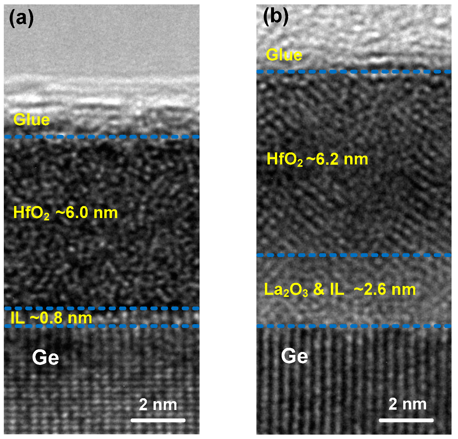
Additional microstructure information of the deposited films is provided by cross-sectional HRTEM analysis as shown in Figure 3. For the control sample without La2O3 passivation layer, the HfO2 layer exhibits an amorphous structure as no nanometer-sized crystal or long-range ordered crystal region is observed. However, in sample S4 with 15 ALD cycles of La2O3 passivation layer (as shown in Figure 3b), nanometer-sized crystals could be observed in the HfO2 layer, indicating the incomplete crystallization state of the HfO2 film. It is noteworthy that upon the same RTA condition at 400 °C for 90 s in N2 ambient, the HfO2 films in sample S1 and S4 show different crystalline characteristics. This difference could be attributed to the RTA-induced Ge diffusion from the substrate into the HfO2 layer as shown in the EDX profiles near the interfaces between the deposited films and Ge substrates (Figure 4). The EDX data were dealt with normalization method after eliminating the influence of impurity elements, and the depth values were calibrated by HRTEM results. During the RTA process, in sample S1 as shown in Figure 4a, the substrate Ge atoms would diffuse easily to the upper HfO2 layer and react with the oxygen nearby the HfO2/Ge interface, which would prevent the formation of crystalline HfO2 precipitates [20] and cause the formation of IL (~0.8 nm) consisting of HfGeOx and GeOx, as analyzed in the above XPS results. As for the HfO2/La2O3/Ge structure in sample S4 (Figure 4b), due to the high affinity of La2O3 for Ge atoms [21], the out-diffused Ge atoms would react with La2O3 passivation layer, leading to the spontaneous formation of stable LaGeOx IL. As a result, few Ge atoms would diffuse into the HfO2 layer, and the crystallization phenomenon occurs after the RTA treatment.
3.3. Surface Morphology of HfO2 and HfO2/La2O3 Gate Stacks on Ge Substrates
The AFM images of HfO2/La2O3 gate stacks on Ge substrates with 0, 5, 10, and 15 ALD cycles of La2O3 interfacial passivation layer are shown in Figure 5. The scan size of each AFM image was set as 10 × 10 µm2. The AFM images were captured from the AFM data by the software named Gwyddion. The root mean square (RMS) roughness of samples S1~S4 is extracted to be 0.63, 0.51, 0.28, and 0.25 nm, respectively. The small RMS roughness values of all the samples illustrate the smooth and crack-free surfaces of the deposited HfO2/La2O3 gate stacks, indicating that ALD is a good deposition method for high-k dielectric films and stacks. On the basis of the smooth surfaces, a decrease in the RMS roughness values is observed after inserting a La2O3 interfacial passivation layer, and the RMS roughness values decrease with the increase of La2O3 layer thickness. It has been reported that the outdiffused Ge atoms from substrates and the desorption of volatile species GeO during the high temperature annealing process could bring in large roughness [22]. After inserting La2O3 interfacial passivation layer, the stable LaGeOx layer could suppress the formation of unstable GeOx layer, which contributes to the decrease of the RMS roughness value. With the increase of La2O3 thickness, more La2O3 reacts with the outdiffused Ge atoms and unstable Ge oxides, which effectively suppresses desorption from GeO2 to volatile GeO, resulting in a smoother surface. It is found that when the thickness of La2O3 layer increase above 15 cycles, the variation in the RMS roughness values becomes negligible. The variation tendency of RMS roughness illustrates that 15 ALD cycles of La2O3 layer are thick enough to improve the surface smoothness for HfO2/Ge structures.
3.4. Electrical Performance of Al/HfO2/Ge and Al/HfO2/La2O3/Ge MIS Capacitors
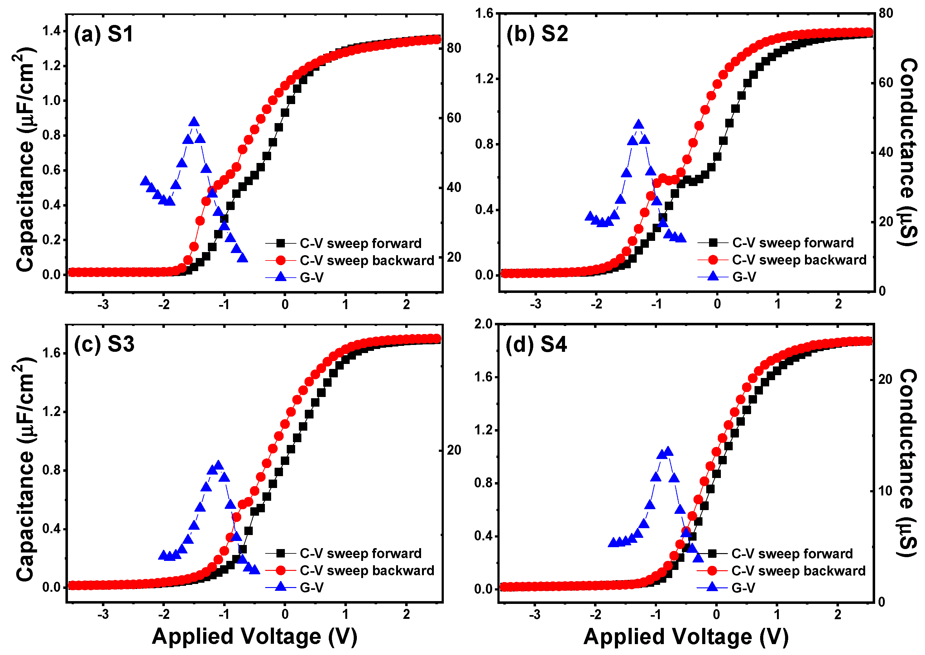
The capacitance-voltage (C-V) and conductance-voltage (G-V) characteristics of the fabricated Al/HfO2/n-Ge and Al/HfO2/La2O3/n-Ge MIS capacitors are shown in Figure 6. Dual-swept C-V curves were obtained by sweeping from inversion to accumulation (forward) and sweeping back (backward) at the frequency of 100 kHz. G-V curves were obtained simultaneously with the C-V curves measured forward. To quantitatively characterize the effects of La2O3 passivation layer thickness on electrical performance of HfO2/Ge MOS structures, some parameters are extracted from the dual-swept C-V curves. The accumulation capacitance (Cac) values for gate stacks S1~S4 are obtained to be 1.35, 1.48, 1.69, and 1.87 μF/cm2, respectively. Then, the oxide capacitance (Cox) and dielectric constant values of gate stacks could be calculated following the equations [23,24]:
where Cac is the capacitance value at accumulation region, Gac is the conductance corresponding to the accumulation region of the C-V curves, ω is the angular frequency, Cox is the oxide capacitance of gate stacks, A is the area of the top electrode, CET is the capacitance equivalent thickness of deposited gate stacks (including IL), tox is the measured thickness of deposited gate stacks (including IL), ε0 and εSiO2 are the permittivity values of vacuum and SiO2, respectively. The physical thickness of gate stacks (including IL) in S1, S2, S3, and S4 is optically measured to be 6.71, 7.89, 8.26, and 8.95 nm, respectively. The corresponding 95% confidence interval for the average thickness of the deposited films was shown in Table S1 in the Supplementary Materials to evaluate the discrete degree of thickness testing data. Therefore, according to Equations (1)–(3), the effective k values of S1~S4 are achieved to be 10.69, 13.43, 15.97, and 18.46, respectively. It is found that the dielectric constant value of HfO2/La2O3 gate stacks increases with the increase of La2O3 layer thickness. The improvement on the value of dielectric constant for the gate stacks is attributed to the effective suppression of Ge atoms outdiffusion benefiting from the generation of stable LaGeOx, since the k value of La2O3 is much higher than that of GeOx [25]. In addition, as analyzed in the EDX profiles, the HfO2 quality is improved by La2O3 passivation, which should be the other cause that increases the dielectric constant of the deposited films.
Moreover, as shown in Figure 6, varying degrees of anomalous humps in the weak inversion region of C-V curves could be observed. Compared with the control sample (Figure 6a), the anomalous hump phenomenon turns more serious after inserting 5 ALD cycles of La2O3 passivation layer. While with the further increase of La2O3 passivation layer thickness, the humps of C-V curves are obviously reduced. Besides, as the thickness of La2O3 passivation layer increases, different degrees of frequency dispersion phenomenon at the weak inversion regions could be observed from the multi-frequency C-V curves in Figure 7, and the degrees of frequency dispersion phenomenon show a similar variation tendency with the anomalous humps in the C-V curves measured at 100 kHz. It has been reported that the existence of slow interface traps (Qit) should be responsible for the anomalous phenomenon at the weak inversion regions of C-V curves [26,27]. Considering this, the interface state density (Dit) values of S1~S4 are discussed using the following relation of single-frequency approximation method through the forward swept C-V and G-V curves [28]:
where q is the elementary charge (1.602 × 10⁻¹⁹ C), A is the area of the top electrode, Cox is the gate oxide capacitance as defined in Equation (1), Gmax is the peak value of G-V curve, and Cmax is the capacitance corresponding to Gmax at the same gate applied voltage. Following Equation (4), the Dit values for the fabricated MIS capacitors using S1~S4 as insulators are calculated to be 9.18 × 10¹², 9.72 × 10¹², 3.95 × 10¹², and 2.71 × 10¹² eV−1cm−2, respectively. The Dit value increases slightly after inserting 5 ALD cycles of La2O3 passivation layer, which is in consistent with the variation tendency of the humps in C-V curves. The increment of Dit is reported to be caused by an incomplete reaction of the precursor molecules during the first few ALD cycles [29], which brings in extra interface states at the interface. As the ALD cycles of La2O3 passivation layer increase, the improvement of the La2O3 passivation layer on the interfacial properties of gate insulators/Ge interfaces plays a more and more important role, contributing to the decrease of interface traps for the samples S3 and S4. For accuracy, the Dit values were also extracted using conductance method [30] measured from 1 kHz to 1 MHz, as shown in Figure 8. It could be observed that for each energy state, the Dit value extracted by conductance method increases slightly after inserting 5 ALD cycles of La2O3 passivation layer, while with the further increase of La2O3 passivation layer thickness, the Dit value shows decrease trend. This result is in good consistency with the single-frequency approximation method result. The contribution of the La2O3 interfacial passivation layer to the amount of interface traps at the La2O3/Ge interface could be explained as follows: during the ALD process of La(i-PrCp)3 and H2O precursors and the high temperature PDA process, La2O3 is more likely to react with outdiffused Ge atoms and Ge oxides nearby the interface to form stable LaGeOx compound. The stable LaGeOx compound could effectively suppress Ge outdiffusion, and further inhibit the decomposition or desorption from GeO2 to volatile GeO (following the reaction equation of GeO2 + Ge → 2GeO), contributing to the reduction of structural defects and dangling bonds [31,32]. The Dit value (2.71 × 10¹² eV−1cm−2) of sample S4 achieved in our work is comparable with the results obtained in the reported literatures at La2O3/Ge interfaces of 3 × 10¹² [8] and 3.5 × 10¹² eV−1cm−2 [25], indicating that a La2O3 passivation layer with 15 ALD cycles (~1.3 nm) can effectively suppress the generation of interface states at high k dielectrics/Ge interfaces.
It is also observed from the C-V curves that the flat band voltages (VFB) translate toward positive voltages with the increase of La2O3 passivation layer deposition cycles. To further investigate this phenomenon in detail, the VFB values of the capacitors were extracted using the Hauser NCSU CVC simulation software taking into account of quantum-mechanical effects [33]. Considering the work function difference between the top electrode aluminum and the n-type Ge substrate with a doping concentration of 1 × 1016 cm−3, the ideal VFB should be 0.03 V. However, the actual VFB swept forward for the control sample is −0.206 V. The negative VFB shift indicates the existence of effective positive oxide charges in the HfO2 film. The effective positive oxide charges may be attributed to the existence of positive fixed oxide charges and oxide trapped charges mainly consisting of oxygen vacancies and structural defects in the gate insulators and/or nearby the insulators/Ge interface. Compared with the control sample, the forward swept VFB values of MIS capacitors S2~S4 were extracted to be −0.083, −0.071, and −0.048 V, separately. The positive shifts of VFB with the increase of La2O3 passivation layer thickness reveal the reduction of oxide charges after the Ge surface passivation treatment using La2O3 as the passivation layer. Considering this, the trapped charge density (Not) is estimated using the midgap charge separation method through the C-V hysteresis characteristics following the Equation (5) [34]:
where ΔVFB is the hysteresis width of VFB, Cox is the oxide capacitance, q is the elementary charge (1.602 × 10⁻¹⁹ C), and A is the area of the electrode. For the control sample, using the exacted ΔVFB value of 685 mV, a trapped oxide charge density of 6.03 × 1012 cm−2 is obtained according to Equation (5). After the insertion of La2O3 passivation layer, the trapped oxide charge densities of samples S2, S3 and S4 are calculated to be 4.74 × 10¹², 2.87 × 10¹², and 1.79 × 1012 cm−2, respectively. These parameter results concerning the electrical properties are summarized in Table 1. As suspected, the trapped oxide charge density reduces with the increase of La2O3 thickness. We ascribe the decrease of trapped charges to the reduction of oxygen vacancies and structural defects in the gate stack region nearby the interface. At the HfO2/Ge interface, the outdiffused Ge atoms will react with GeO2 to form unstable GeO, which could bring in a large number of oxygen vacancies and structural defects. The LaGeOx compound formed by La2O3 and Ge could effectively suppress the outdiffusion of Ge atoms and the desorption of volatile GeO, contributing to the reduction of Not values.
Figure 9 shows the gate leakage current density as a function of the applied effective field for samples S1~S4. It is observed that the gate leakage current density of gate insulator/Ge structures obviously decreases with the increase of La2O3 layer thickness. At the applied effective field of 3 MV/cm, compared with the control sample, in the sample S4 the gate leakage current density decreases of almost an order of magnitude. The obvious decrease in the gate leakage current density could be ascribed to the reduction in the structural defects in the HfO2/La2O3 gate stack benefiting from the generation of stable LaGeOx component. Moreover, the gate leakage current density-voltage (J-V) characteristics show different breakdown behaviors, which suggests that the incorporation of La2O3 interfacial passivation layer improves the breakdown field strength of HfO2/Ge MIS capacitors. The improvement of the breakdown field strength is reported to be associated with a reduction in defects in gate dielectrics [35]. As mentioned above, the existence of La2O3 interfacial passivation layer could effectively suppress the generation of structural defects, oxygen vacancies and dangling bonds. The reduction of structural defects, oxygen vacancies and dangling bonds decreases the possibility to create a conduction path by forming a continuous chain connecting the gate to the semiconductor, resulting in higher breakdown field.
4. Conclusions
In summary, we investigate the effect of La2O3 passivation layer thickness on the interfacial and electrical properties of HfO2/Ge MIS structures. It is found that the gate leakage current density of the MIS capacitor after inserting 15 ALD cycles (~1.3 nm) of La2O3 passivation layer gains almost one order of magnitude decrease than that of the Al/HfO2/Ge MIS sample. Besides, a relatively low Dit value of 2.71 × 10¹² eV−1cm−2 is achieved. The thickness of the La2O3 passivation layer also affects the dielectric constants, VFB shifts, hysteresis behaviors and the shapes of dual-swept C-V curves. The improvement on the interfacial and electrical properties with the increase of La2O3 passivation layer deposition cycles is related to the formation of a stable LaGeOx layer on the Ge surface, which restrains the decomposition or desorption from GeO2 to volatile GeO, contributing to the decrease of structural defects. These results provide us with quite an effective method for realizing high-quality dielectric/Ge interfaces for Ge-based MIS devices.
Supplementary Materials
The following are available online at https://www.mdpi.com/2079-4991/9/5/697/s1, Table S1: Thickness of the deposited films (including interfacial layer) on Ge substrates.
Author Contributions
L.Z. generated the research idea, analyzed the data, and wrote the paper. L.Z. and Y.W. carried out the experiments and the measurements. S.W. participated in the discussions. H.L. and X.W. have given final approval of the version to be published. All authors read and approved the final manuscript.
Funding
This research was funded by the National Natural Science Foundation of China (Grant No. U1866212), the Foundation for Fundamental Research of China (Grant No. JSZL2016110B003), the China Postdoctoral Science Foundation (Grant No. 2018M633460), and the 111 project (Grant No. B12026).
Acknowledgments
The authors gratefully acknowledge the support provided by the Fundamental Research Funds for the Central Universities and the Innovation Fund of Xidian University.
Conflicts of Interest
The authors declare no conflict of interest.
References
- Lee, B.H.; Oh, J.; Tseng, H.H.; Jammy, R.; Huff, H. Gate Stack Technology for Nanoscale Devices. Mater. Today 2006, 9, 32–40. [Google Scholar] [CrossRef]
- Kamata, Y. High-K/Ge MOSFETs for Future Nanoelectronics. Mater. Today 2008, 11, 30–38. [Google Scholar] [CrossRef]
- Yi, S.H.; Chang-Liao, K.S.; Wu, T.Y.; Hsu, C.W.; Huang, J.Y. High Performance Ge pMOSFETs with HfO2/Hf-Cap/GeOx Gate Stack and Suitable Post Metal Annealing Treatments. IEEE Electron Device Lett. 2017, 38, 544–547. [Google Scholar] [CrossRef]
- Simoen, E.; Mitard, J.; Hellings, G.; Eneman, G.; DeJaeger, B.; Witters, L.; Vincent, B.; Loo, R.; Delabie, A.; Sioncke, S.; et al. Challenges and Opportunities in Advanced Ge pMOSFETs. Mater. Sci. Semicond. Process. 2012, 15, 588–600. [Google Scholar] [CrossRef]
- Houssa, M.; Chagarov, E.; Kummel, A. Surface Defects and Passivation of Ge and III–V Interfaces. MRS Bull. 2009, 34, 504–513. [Google Scholar] [CrossRef]
- Kouda, M.; Suzuki, T.; Kakushima, K.; Ahmet, P.; Iwai, H.; Yasuda, T. Electrical Properties of CeO2/La2O3 Stacked Gate Dielectrics Fabricated by Chemical Vapor Deposition and Atomic Layer Deposition. Jpn. J. Appl. Phys. 2012, 51, 121101. [Google Scholar]
- Liu, Q.Y.; Fang, Z.B.; Liu, S.Y.; Tan, Y.S.; Chen, J.J. Band Offsets of La2O3 Films on Ge Substrates Grown by Radio Frequency Magnetron Sputtering. Mater. Lett. 2014, 116, 43–45. [Google Scholar] [CrossRef]
- Abermann, S.; Bethge, O.; Henkel, C.; Bertagnolli, E. Atomic Layer Deposition of ZrO2/La2O3 High-K Dielectrics on Germanium Reaching 0.5 Nm Equivalent Oxide Thickness. Appl. Phys. Lett. 2009, 94, 262904. [Google Scholar] [CrossRef]
- Calmels, L.; Coulon, P.E.; Schamm-Chardon, S. Calculated and Experimental Electron Energy-Loss Spectra of La2O3, La(OH)3, and LaOF Nanophases in High Permittivity Lanthanum-Based Oxide Layers. Appl. Phys. Lett. 2011, 98, 243116. [Google Scholar] [CrossRef]
- Zhao, L.; Liu, H.X.; Wang, X.; Wang, Y.T.; Wang, S.L. Improvements on the Interfacial Properties of High-K/Ge MIS Structures by Inserting a La2O3 Passivation Layer. Materials 2018, 11, 2333. [Google Scholar] [CrossRef]
- Eom, D.; Hwang, C.S.; Kim, H.J. Thermal Stability of Stack Structures of Aluminum Nitride and Lanthanum Oxide Thin Films. ECS Trans. 2006, 3, 121–127. [Google Scholar]
- Hausmann, D.M.; Kim, E.; Becker, J.; Gordon, R.G. Atomic Layer Deposition of Hafnium and Zirconium Oxides Using Metal Amide Precursors. Chem. Mater. 2002, 14, 4350–4358. [Google Scholar] [CrossRef]
- Cao, D.; Cheng, X.H.; Yu, Y.H.; Li, X.L.; Liu, C.Z.; Shen, D.S.; Mändl, S. Competitive Si and La Effect in HfO2 Phase Stabilization in Multi-Layer (La2O3)0.08(HfO2) Films. Appl. Phys. Lett. 2013, 103, 081607. [Google Scholar] [CrossRef]
- Mitrovic, I.Z.; Althobaiti, M.; Weerakkody, A.D.; Sedghi, N.; Hall, S.; Dhanak, V.R.; Chalker, P.R.; Henkel, C.; Dentoni, L.E.; Hellström, P.E.; et al. Interface Engineering of Ge Using Thulium Oxide: Band Line-Up Study. Microelectron. Eng. 2013, 109, 204–207. [Google Scholar] [CrossRef]
- Song, J.; Kakushima, K.; Ahmet, P.; Tsutsui, K.; Sugii, N.; Hattori, T.; Iwai, H. Improvement of Interfacial Properties with Interfacial Layer in La2O3/Ge Structure. Microelectron. Eng. 2007, 84, 2336–2339. [Google Scholar] [CrossRef]
- Li, X.F.; Liu, X.J.; Cao, Y.Q.; Li, A.D.; Li, H.; Wu, D. Improved Interfacial and Electrical Properties of Atomic Layer Deposition HfO2 Films on Ge with La2O3 Passivation. Appl. Surf. Sci. 2013, 264, 783–786. [Google Scholar] [CrossRef]
- Kim, H.C.; Woo, S.H.; Lee, J.S.; Kim, H.G.; Kim, Y.C.; Lee, H.R.; Jeon, H.T. The Effects of Annealing Ambient on the Characteristics of La2O3 Films Deposited by RPALD. J. Electrochem. Soc. 2010, 157, H479–H482. [Google Scholar] [CrossRef]
- Mitrovic, I.Z.; Althobaiti, M.; Weerakkody, A.D.; Dhanak, V.R.; Linhart, W.M.; Veal, T.D.; Sedghi, N.; Hall, S.; Chalker, P.R.; Tsoutsou, D.; et al. Ge Interface Engineering Using Ultra-Thin La2O3 and Y2O3 Films: A Study into the Effect of Deposition Temperature. J. Appl. Phys. 2014, 115, 114102. [Google Scholar] [CrossRef]
- Schmeisser, D.; Schnell, R.D.; Bogen, A.; Himpsel, F.J.; Rieger, D.; Landgren, G.; Morar, J.F. Surface Oxidation States of Germanium. Surf. Sci. 1986, 172, 455–465. [Google Scholar] [CrossRef]
- Wilka, G.D.; Wallace, R.M. Electrical Properties of Hafnium Silicate Gate Dielectrics Deposited Directly on Silicon. Appl Phys Lett. 1999, 74, 2854–2856. [Google Scholar] [CrossRef]
- Lin, M.H.; Lan, C.K.; Chen, C.C.; Wu, J.Y. Electrical Properties of HfO2/La2O3 Gate Dielectrics on Ge with Ultrathin Nitride Interfacial Layer Formed by in Situ N2/H2/Ar Radical Pretreatment. Appl. Phys. Lett. 2011, 99, 182105. [Google Scholar] [CrossRef]
- Wang, S.K.; Kita, K.; Lee, C.H.; Tabata, T.; Nishimura, T.; Nagashio, K.; Toriumi, A. Desorption Kinetics of GeO from GeO2/Ge Structure. J. Appl. Phys. 2010, 105, 054104. [Google Scholar]
- Bhaisare, M.; Misra, A.; Kottantharayil, A. Aluminum Oxide Deposited by Pulsed-DC Reactive Sputtering for Crystalline Silicon Surface Passivation. IEEE J. Photovolt. 2013, 3, 930–935. [Google Scholar] [CrossRef]
- Cao, D.; Cheng, X.H.; Jia, T.T.; Xu, D.W.; Wang, Z.J.; Xia, C.; Yu, Y.H. Characterization of HfO2/La2O3 Layered Stacking Deposited on Si Substrate. J. Vac. Sci. Technol. B. Nanotechnol. Microelectron. 2013, 31, 01A113. [Google Scholar] [CrossRef]
- Lamagna, L.; Wiemer, C.; Perego, M.; Volkos, S.N.; Baldovino, S.; Tsoutsou, D.; Schamm-Chardon, S.; Coulon, P.E.; Fanciulli, M. O3-Based Atomic Layer Deposition of Hexagonal La2O3 films on Si (100) and Ge (100) Substrates. J. Appl. Phys. 2010, 108, 084108. [Google Scholar] [CrossRef]
- Martens, K.; Chui, C.O.; Brammertz, G.; Jaeger, B.D.; Kuzum, D.; Meuris, M.; Heyns, M.M.; Krishnamohan, T.; Saraswat, K.; Maes, H.E.; et al. On the Correct Extraction of Interface Trap Density of MOS Devices with High-Mobility Semiconductor Substrates. IEEE Trans. Electron Device 2008, 55, 547–556. [Google Scholar] [CrossRef]
- Suzuki, T.; Kouda, M.; Ahmet, P.; Iwai, H.; Kakushima, K.; Yasuda, T. La2O3 Gate Insulators Prepared by Atomic Layer Deposition: Optimal Growth Conditions and MgO/La2O3 Stacks for Improved Metal-Oxide-Semiconductor Characteristics. J. Vac. Sci. Technol. A 2012, 30, 051507. [Google Scholar] [CrossRef]
- Hill, W.A.; Coleman, C.C. A Single-Frequency Approximation for Interface-State Density Determination. Solid State Electron. 1980, 23, 987–993. [Google Scholar] [CrossRef]
- Stesmans, A.; Afanas’ev, V.V. Si Dangling-Bond-Type Defects at the Interface of (100) Si with Ultrathin Layers of SiOx, Al2O3, and ZrO2. Appl. Phys. Lett. 2002, 80, 1957. [Google Scholar] [CrossRef]
- Engel-Herbert, R.; Hwang, Y.; Stemmer, S. Comparison of Methods to Quantify Interface Trap Densities at Dielectric/III–V Semiconductor Interfaces. J. Appl. Phys. 2010, 108, 124101. [Google Scholar] [CrossRef]
- Bethge, O.; Zimmermann, C.; Lutzer, B.; Simsek, S.; Abermann, S.; Bertagnolli, E. ALD Grown Rare-Earth High-K Oxides on Ge: Lowering of the Interface Trap Density and EOT Scalability. ECS Trans. 2014, 64, 69–76. [Google Scholar] [CrossRef]
- Kita, K.; Suzuki, S.; Nomura, H.; Takahashi, T.; Nishimura, T.; Toriumi, A. Direct Evidence of GeO Volatilization from GeO2/Ge and Impact of Its Suppression on GeO2/Ge Metal-Insulator-Semiconductor Characteristics. Jpn. J. Appl. Phys. 2008, 47, 2349–2353. [Google Scholar] [CrossRef]
- Hauser, J.R.; Ahmed, K. Characterization of Ultra-Thin Oxides Using Electrical C-V and I-V Measurements. AIP Conf. Proc. 1998, 445, 235. [Google Scholar]
- SZE, S.M.; NG, K.K. Physics of Semiconductor Devices, 3rd ed.; John Wiley & Sons Inc.: Hoboken, NJ, USA, 2006; pp. 223–236. [Google Scholar]
- Spahr, H.; Bülow, T.; Nowak, C.; Hirschberg, F.; Reinker, J.; Hamwi, S.; Johannes, H.H.; Kowalsky, W. Impact of Morphological Defects on the Electrical Breakdown of Ultra-Thin Atomic Layer Deposition Processed Al2O3 Layers. Thin Solid Films 2013, 534, 172–176. [Google Scholar] [CrossRef]
Figure 1.
O 1s XPS spectra of HfO2 film and HfO2/La2O3 gate stacks deposited on Ge substrates.

Figure 2.
Ge 3d XPS spectra of the deposited gate stacks with different ALD cycles of La2O3 passivation layer on Ge substrates. (a) The control sample; (b) 5 ALD cycles of La2O3 passivation layer; (c) 10 ALD cycles of La2O3 passivation layer; and (d) 15 ALD cycles of La2O3 passivation layer.
Figure 2.
Ge 3d XPS spectra of the deposited gate stacks with different ALD cycles of La2O3 passivation layer on Ge substrates. (a) The control sample; (b) 5 ALD cycles of La2O3 passivation layer; (c) 10 ALD cycles of La2O3 passivation layer; and (d) 15 ALD cycles of La2O3 passivation layer.

Figure 3.
Cross-sectional HRTEM images showing the interfaces with Ge substrates for (a) the control sample; (b) sample S4 with 15 ALD cycles of La2O3 passivation layer.
Figure 3.
Cross-sectional HRTEM images showing the interfaces with Ge substrates for (a) the control sample; (b) sample S4 with 15 ALD cycles of La2O3 passivation layer.

Figure 4.
EDX profiles near the interfaces between the deposited films and Ge substrates. (a) the control sample; (b) sample S4 with 15 ALD cycles of La2O3 passivation layer.
Figure 4.
EDX profiles near the interfaces between the deposited films and Ge substrates. (a) the control sample; (b) sample S4 with 15 ALD cycles of La2O3 passivation layer.

Figure 5.
Three-dimensional AFM images of the deposited gate stacks with different ALD cycles of La2O3 passivation layer on Ge substrates. (a) The control sample; (b) 5 ALD cycles of La2O3 passivation layer; (c) 10 ALD cycles of La2O3 passivation layer; and (d) 15 ALD cycles of La2O3 passivation layer.
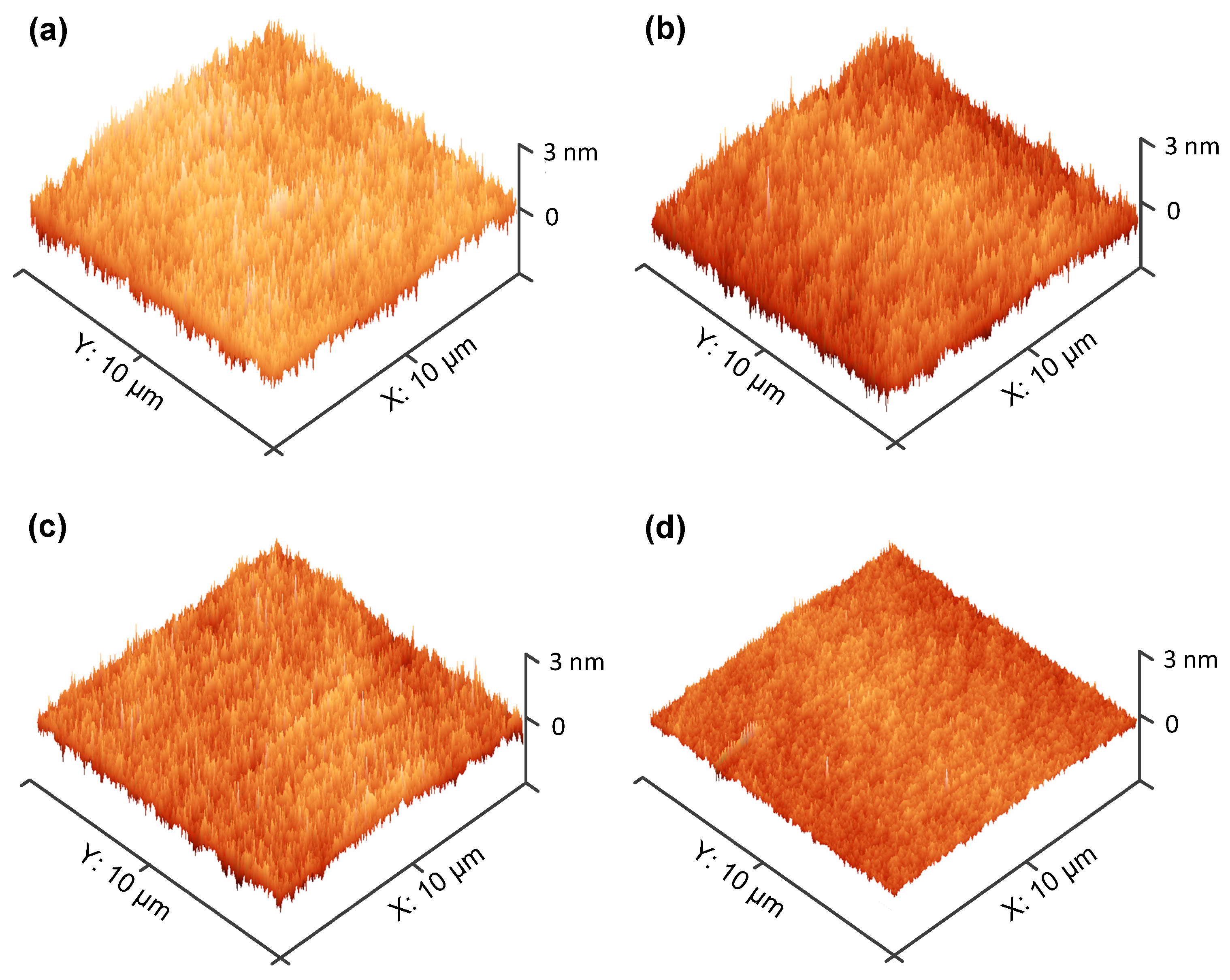
Figure 6.
C-V curves and G-V characteristics of the fabricated Al/HfO2/La2O3/Ge MIS capacitors with different ALD cycles of La2O3 passivation layer. (a) The control sample; (b) 5 ALD cycles of La2O3 passivation layer; (c) 10 ALD cycles of La2O3 passivation layer; and (d) 15 ALD cycles of La2O3 passivation layer. The curves were measured at the frequency of 100 kHz.

Figure 7.
Multi-frequency C-V characteristics measured of the fabricated Al/HfO2/La2O3/Ge MIS capacitors with different ALD cycles of La2O3 passivation layer. (a) The control sample; (b) 5 ALD cycles of La2O3 passivation layer; (c) 10 ALD cycles of La2O3 passivation layer; and (d) 15 ALD cycles of La2O3 passivation layer.

Figure 8.
Energy distribution of the interface states at the interface between the deposited films and Ge substrates.
Figure 8.
Energy distribution of the interface states at the interface between the deposited films and Ge substrates.

Figure 9.
J–V characteristics of Al/HfO2/Ge and Al/HfO2/La2O3/Ge MIS capacitors.


Table 1.
The electrical parameters extracted from the fabricated MIS capacitors without and with La2O3 interfacial passivation layers.
Table 1.
The electrical parameters extracted from the fabricated MIS capacitors without and with La2O3 interfacial passivation layers.
| Sample | Cox (µF/cm2) | k | △VFB (mV) | Dit (eV−1cm−2) | Not (cm−2) |
|---|---|---|---|---|---|
| S1 | 1.411 | 10.69 | 685 | 9.18 × 10¹² | 6.03 × 10¹² |
| S2 | 1.510 | 13.43 | 504 | 9.72 × 10¹² | 4.74 × 10¹² |
| S3 | 1.712 | 15.97 | 269 | 3.95 × 10¹² | 2.87 × 10¹² |
| S4 | 1.883 | 18.46 | 152 | 2.71 × 10¹² | 1.79 × 10¹² |
© 2019 by the authors. Licensee MDPI, Basel, Switzerland. This article is an open access article distributed under the terms and conditions of the Creative Commons Attribution (CC BY) license (http://creativecommons.org/licenses/by/4.0/).
Share and Cite
MDPI and ACS Style
Zhao, L.; Liu, H.; Wang, X.; Wang, Y.; Wang, S. Electrical Properties and Interfacial Issues of HfO2/Ge MIS Capacitors Characterized by the Thickness of La2O3 Interlayer. Nanomaterials 2019, 9, 697. https://doi.org/10.3390/nano9050697
AMA Style
Zhao L, Liu H, Wang X, Wang Y, Wang S. Electrical Properties and Interfacial Issues of HfO2/Ge MIS Capacitors Characterized by the Thickness of La2O3 Interlayer. Nanomaterials. 2019; 9(5):697. https://doi.org/10.3390/nano9050697
Chicago/Turabian StyleZhao, Lu, Hongxia Liu, Xing Wang, Yongte Wang, and Shulong Wang. 2019. "Electrical Properties and Interfacial Issues of HfO2/Ge MIS Capacitors Characterized by the Thickness of La2O3 Interlayer" Nanomaterials 9, no. 5: 697. https://doi.org/10.3390/nano9050697
Note that from the first issue of 2016, this journal uses article numbers instead of page numbers. See further details here.