Tunable Duplex Metalens Based on Phase-Change Materials in Communication Range
by
 ,
,
Wei Bai
1,2,3,4, 
Ping Yang
1,3,
Shuai Wang
1,3,
Jie Huang
2,
Dingbo Chen
2,
Zhaojian Zhang
2,
Junbo Yang
2,* and
Bing Xu
1,3,* 1
The Key Laboratory of Adaptive Optics, Chinese Academy of Sciences, Chengdu 610209, China
2
Center of Material Science, National University of Defense Technology, Changsha 410073, China
3
Institute of Optics and Electronics, Chinese Academy of Sciences, Chengdu 610209, China
4
University of Chinese Academy of Sciences, Beijing 100049, China
*
Authors to whom correspondence should be addressed.
Nanomaterials 2019, 9(7), 993; https://doi.org/10.3390/nano9070993
Submission received: 30 May 2019
/
Revised: 6 July 2019
/
Accepted: 9 July 2019
/
Published: 10 July 2019
(This article belongs to the Special Issue Nanophotonics and Its Applications)
Abstract
:Metalenses recently have attracted attention because of their more compact size in comparison with conventional lenses; they can also achieve better optical performance with higher resolution. Duplexer is an interesting function of a metalens that can distinguish different sources and divide them into two parts for specific purposes. In this article, we design tunable duplex metalenses with phase-change material Ge2Sb2Te5 for the first time. Two types of special unit cells are designed to modulate the incident lights, and four metalenses are designed based on the two types of unit cells. Specific phase profiles are calculated for different sections of metalens in which the corresponding unit cells are settled; accordingly, the metalenses can focus the incident lights at any positions according to our design. Moreover, the metalenses become selectable via tuning the state of phase-change material, which means that the output light field can be actively controlled. The proposal of our tunable duplex metalenses will offer new opportunities for active three-dimensional imaging or optical coding.
1. Introduction
Recently, researchers have begun to pay increasing attention to metasurfaces due to their extraordinary performance in electromagnetism fields [1,2,3,4,5,6,7,8,9,10,11,12,13,14,15,16,17,18,19,20,21]. As 2D, artificial, photonic metamaterials, metasurfaces can manipulate the electromagnetic wave freely. By shaping the subwavelength resonators of metasurfaces, the amplitude, phase, polarization, and propagation direction of light can be easily controlled [1,2,3,4]. With the completion of new theories and technologies in this field, they have been applied to various functions, such as to ultrathin metalens [5,6], cloaking [7,8], nonlinear device [9,10], holograms [11,12], surface plasmon launcher [13], computing [14,15], biosensing [16,17], switching [18,19] and many novel photonic devices [20,21]. Metalens has become an exciting research topic that holds great promise to the applications of metasurfaces. Metalens can not only show better optical performance but also be smaller and lighter, which is more suitable for compact devices in comparison with conventional lens. Recently, excellent research about metalens have been reported. For example, Khorasaninejad et al. verified the exceptional ability of metalens experimentally [5]. Also, other functions such as chromatic aberration correction [6,22,23,24] and active tuning [25,26,27] have been proposed or proved. However, there are still various functions to be achieved, owing to the subwavelength manipulation to the electromagnetic field.
Duplexer can divide a light source into two parts for distinct uses. Using this as inspiration, we can design duplex metalens that can separate light sources and focus or image them at designed positions, which is impossible for conventional lenses. This is especially important in beam splitter or three-dimensional imaging. Some previous efforts have explored the novel functions of metalens. For instance, Li et al. focused light with different wavelengths into different positions [28], and Boroviks et al. focused different polarized lights into different positions [29]. Nevertheless, once metalenses are fabricated, the functions are fixed, which makes them inflexible. However, this situation can be improved with the help of tunable phase-change materials.
Phase-change materials have been applied in optical disk storage for many years. Recently, they have been increasingly used for electrical nonvolatile memories in which their refractive index can be selectively tuned [30,31,32]. As a typical phase-change material, Ge2Sb2Te5 (GST) alloy has two different states: the amorphous state and the crystalline state. Different phase states correspond to different lattice arrangements such as amorphous, metastable, face-centered cubic (Fcc), and stable hexagon, all of which result in great complex permittivity contrast at near-infrared (NIR) and middle-infrared (MIR). Especially, the state transition between amorphous and crystalline can be precisely controlled by appropriate thermal, optical, or electrical stimuli [30,31,32]. The amorphous GST is gradually crystallized when it is heated to the temperature between the transition temperature (160 °C) and the melting temperature (627 °C) [33]. After a short, high-density laser pulse melts the GST and is it quickly quenched, the crystallized GST returns to an amorphous state (the reamorphization temperature is 640 °C) [34]. GST has become the most promising candidate for the next generation of controllable, nonvolatile photonic devices due to its ultrafast switching speed (occurring in a nanosecond or less) [32], high-switching stability (potentially up to 1015 cycles) [35], and compatibility with Complementary Metal Oxide Semiconductor (CMOS) technology. Lately, the combination of GST with metasurfaces has attracted increasing interest because active control is desirable in many nano-photonic devices. Several metadevices, such as display [36], filter [37], absorber [38], beam steering [39], modulation [40,41,42] and other novel devices [34,43,44,45,46], all of which are based on phase change materials, have been investigated. All devices have demonstrated the great potentialities of GST in active and flexible control of nano-devices.
In this work, we design the tunable duplex metalens based on phase-change material GST in the communication wavelengths (1.55 μm and 1.31 μm) for the first time. Two unit cells and four metalenses have been designed to test our method. The metalenses are composed of a series of well-designed GST nanocube resonators accompanying Pancharatnam-Berry (P-B) phase shift. Importantly, the metalenses were divided into two sections, and different sections were arranged with different unit cells to achieve duplex function. When the GST structures remained at the amorphous state, the corresponding light was able to pass through. When the GST structures stayed at the crystalline state, the corresponding light was shut off. Accordingly, we can selectively control the focused light on demand by adjusting the state of GST when the incident light is 1.31 μm, 1.55 μm, or both. We believe that the proposed tunable duplex metalens could be applied in active three-dimensional imaging or optical coding.
2. Single-Wavelength Tunable Duplex Metalenses
The structure of the unit cell is depicted in Figure 1a. A nanocuboid waveguide GST was placed on the transparent SiO2 substrate. The orientation of GST formed an angle θ with x axis as shown in Figure 1b; Figure 1c is the side view of the unit cell. A 30-nm thin transparent film of indium tin oxide (ITO) was sandwiched between the GST and the SiO2 substrate. This film was treated as a conductive layer to tune the state of GST by electrically heating the structured GST.
In this work, P-B phase shift is adopted to achieve phase control. A left/right circularly polarization (LCP/RCP) incident light passes through the unit cell, propagating along +z direction; by applying the Jones matrix theory, the output field can be simplified as [28]:
Here, the incident light is the normalized representation of Jones matrix for LCP and RCP separately, and , where to and te represent the complex transmission coefficients along the optical fast axis and slow axis which is determined by the parameters of the unit cell
(p, l, w, h, ε(ω)), and the symbol “” distinguishes the co-polarization and cross-polarization light, respectively. According to the formula, the incident CP light is divided into two cross polarization outputs. The co-polarization light only receives the amplitude modulation but the cross-polarization light has the phase modulation simultaneously. 2π phase tuning can be achieved for the cross-polarization light if the angle rotates from 0 to π. When the state of the GST is changed, the transmission is changed simultaneously; thus the output of the unit cell can be actively controlled.
The simulation of all the unit cells was performed using finite-element method in frequency domain with the unit cell boundary in xy direction and the open boundary in z direction; the minimum size of the mesh was 20 nm. All unit cells were settled in free space. The information of the system used for computing this structures is as follows: The CPU of the system was Intel(R) Xeon(R) CPU E5-2420 v2; the RAM was 24 GB; the duration of the calculation for one unit cell was approximately several minutes; the HDD space was 1.72 TB. In the simulation, the incident LCP plane wave propagated along +z direction through the substrate. The GST data were obtained from the experimental data in reference [47], in which the dielectric function ε(ω) was investigated by infrared spectroscopy and spectroscopic ellipsometry. The conversion efficiency from LCP to RCP and the phase modulation of the unit cell were calculated from the simulations on the unit cell. After optimization at the wavelength of 1.31 μm, the parameters of the unit cell U1 were determined to be p = 600 nm, h =700 nm, l = 230 nm and w = 180 nm. According to the theoretical analysis from Equation (1), a part of incident light will be changed into RCP light with phase modulation of . When , the conversion efficiency from LCP to RCP for two different GST states is shown in Figure 2a. When the GST remained at amorphous state, the conversion efficiency was as high as 87% at the wavelength of 1.31 μm; in contrast, the conversion efficiency was only 16% at the wavelength of 1.55 μm (used for another purpose). When the GST was in crystalline state, the ε(ω) changed and the conversion efficiency was tuned lower than 5%, which can be treated as turning off in the whole range from 1.31 μm to 1.55 μm. Next, the incident light was fixed at 1.31 μm, at which point the angle of structure was rotated from 0 to π; the corresponding phase modulation is shown in Figure 2b. For amorphous GST, the simulation showed no difference with theoretical analysis; however, the phase modulation linearly covered the entire 2π range. Figure 2c shows that the conversion efficiency remained largely unchanged when the angle was rotated from 0 to π, which indicates that the angle had little influence in the conversion efficiency for two different states of GST. All simulations demonstrated that the unit cell is a good candidate for tunable metalens.
To focus like a conventional spherical lens, the phase profile of the metalens should satisfy:
Where λ is the designed wavelength, f is the focal length. (x, y, 0) represents the position of the unit cell, and (xd, yd, f) represents the coordinate of an arbitrary focal point. According to the simulation result of φ = 2θ, the rotating angle of the unit cell in (x, y, 0) should be:
The designed metalens is divided into two equal sections marked as A (x > 0) and B (x < 0). Unit cells U1 were used to construct the metalens M1. Specially, unit cells in section A were arranged as xd = 5 μm, yd = 0, f = 20 μm; unit cells in section B were arranged as xd = −5 μm, yd = 0, f = 20 μm. The radius of the metalens was fixed at 20 μm. The overall structure layout is depicted in Figure 3a. Figure 3b shows the imperfect phase distribution of metalens M1 along the x axis sampling at the center of each unit cell.
The results of all the metalenses were simulated by using finite integrity in time domain and open boundary condition in all directions; the size of the uniform mesh was set at 20 nm along all axes to minimize numerical errors. The entire devices were settled in free space. The duration of the calculation for one metalens was about 24 h (different metalenses spend different time). The light source was set at 1.31 μm LCP plane wave in the simulation. The spatial dimension of incident light is 40 × 40 μm2 and the LCP plane wave can be expressed as:
The incident light was settled at the position lower 1 μm from the metalens. The thickness of the substrate, ITO layer, and GST was 0.2 μm, 0.03 μm, and 0.7 μm, respectively. The output light field was obtained from the position upper 1 μm from the metalens. The spatial dimension of the simulation domain for the full metalens is 40 × 40 × 2.93 μm3. The light field was then exported after finite integrity in time domain and calculated by Matlab with Angular Spectrum Diffraction method in the spatial dimension of 40 × 40 × 40 μm3.
When the GST in both sections remained in an amorphous state, the incident light was separated into two parts: one focused at the position (5.29, 0.32, 19.9) μm, the other focused at the position (−4.64, 0.32, 20.3) μm. The result is illustrated in Figure 4a. Full width at half maximum (FWHM) of the spots in focal plane were 0.95 μm and 0.97 μm, respectively, which indicates that the metalens achieved subwavelength resolution. The deviance from the expected result (5, 0, 20) μm came from the discrete phase distribution, as depicted in Figure 3b. By applying appropriate electrical current pulse through the ITO layer, the state of the GST can be changed. When the GST in section A remained in an amorphous state and the GST in section B was changed into a crystalline state, the incident light was focused at the position (−4.64, 0.32, 20.3) μm with FWHM of 0.95 μm, as shown in Figure 4b. When the GST in section A was changed into a crystalline state while the GST in section B was in an amorphous state, the incident light was focused at the position (5.29, 0.32, 19.9) μm with FWHM of 0.97 μm, as shown in Figure 4c. The result of the GST in both sections changing to a crystalline state is shown in Figure 4d. There was no light focusing because the conversion efficiency from LCP to RCP is very low when GST remains in a crystalline state. The results prove that the focusing effect of our tunable duplex metalens can be actively controlled in horizontal direction and will bring some convenience to integrated optical systems.
Although metalens M1 was designed to have the focus spots arranged in horizontal, in this study, we designed metalens M2 to have the focus spots arranged in vertical. Metalens M2 was also constructed by unit cells U1. Differently, unit cells in section A were arranged as xd = 0, yd = 0, f = 15 μm, and unit cells in section B were arranged as xd = 0, yd = 0, f = 25 μm. The phase distribution of metalens M2 along the x axis is shown in Figure 3c. The conditions of simulation remained unchanged, and the incident light remained 1.31 μm LCP plane wave. When the GST in both sections remained in an amorphous state, the incident light was focused at two different positions: (0.27, 0.27, 15.2) μm and (0.35, 0.35, 24.7) μm. The distribution of light field is depicted in Figure 5a. FWHM of the spot at z = 15.2 μm was 0.83 μm and FWHM of the spot at z = 24.7 μm was 1.03 μm. This is reasonable because longer focal length means smaller numerical aperture (NA), resulting in a larger focal spot. When the GST in section A stayed in an amorphous state and the GST in section B changed to a crystalline state, the incident light was focused at the position (0.27, 0.27, 15.2) μm with FWHM of 0.83 μm, as shown in Figure 5b. When the GST in section A was changed into a crystalline state but the GST in section B remained in an amorphous state, the incident light was focused at the position (0.35, 0.35, 24.7) μm with FWHM of 1.03 μm, as shown in Figure 5c. When the GST in both sections was changed into crystalline state, the metalens was turned off completely, as seen in Figure 5d. These results demonstrate that our tunable duplex metalens can actively control the focusing in vertical direction, and it may have potential in three-dimension imaging.
3. Dual-Wavelength Tunable Duplex Metalenses
When incident light becomes a mixed light of 1.55 μm and 1.31 μm, one single structure apparently can not accomplish the task to distinguish the two different frequencies of lights. Accordingly, another unit cell, U2, needs to be designed to modulate the phase at wavelength of 1.55 μm. The parameters of U2 are determined to be p = 600 nm, h = 700 nm, l = 505 nm, and w = 100 nm after optimization. The same period and height as unit cell U1 was selected to make sure that the different unit cells can be fabricated in the same steps. In this simulation, the LCP plane wave passed through U2 along +z direction. When the angle θ = 0, the conversion efficiency from LCP to RCP for two different states of GST is shown in Figure 6a. When GST stayed at amorphous state, the conversion efficiency was as high as 97% at the wavelength of 1.55 μm; however, the conversion efficiency was only 23% at the wavelength of 1.31 μm. The two unit cells U1 and U2 were designed specially; U1 let the 1.31 μm light pass but turned off the 1.55 μm light whereas U2 let the 1.55 μm light pass but turned off the 1.31 μm light, which will be very useful to separate multi-wavelength incident lights. When the GST stayed in crystalline state, the conversion efficiency was lower than 23% in the range from 1.31 μm to 1.55 μm, which can be treated as turning off in comparison with the effect of the amorphous GST. Next, the incident light was fixed at the wavelength of 1.55 μm. The angle of the structure was rotated from 0 to π, affecting the corresponding phase modulation, as depicted in Figure 6b. The results fit well with theoretical analysis because the phase modulation covers the whole 2π range linearly when the GST stays in amorphous state. Figure 6c demonstrates the relationship between conversion efficiency and the rotating angle, and the results prove that the rotating angle has no influence on the conversion efficiency for unit cell U2.
Metalens M3 is constructed by unit cells U1 and U2 together. Unit cells U1 are arranged in section A as xd = 5 μm, yd = 0, f = 20 μm, and unit cells U2 are arranged in section B as xd = −5 μm, yd = 0, f = 20 μm. Figure 3d is the overview of the metalens, in which the green structures represent U1 and the red structures represent U2. The phase distribution of the metalens M3 along the x axis is depicted in Figure 3e.
In this simulation, the conditions remain unchanged except the incident light source was changed into mixed light of two wavelengths at 1.55 μm and 1.31 μm. When the GST in both sections stayed in an amorphous state, the unit cells in section A and B could allow the light of 1.55 μm and 1.31 μm to pass through, respectively. The incident 1.55 μm light was focused at the position (4.93, 0.38, 20.2) μm with FWHM of 1.12 μm and the incident 1.31 μm light was focused at the position (−4.96, 0.38, 20.1) μm with FWHM of 1.00 μm, which have been marked as red spot and green spot, respectively, as seen in Figure 7a. The size of the spot was proportional to the wavelength while the focal lengths were equal. When the GST in section A stayed in an amorphous state but the GST in section B changed into a crystalline state, only the 1.31 μm incident light was focused at the position (−4.96, 0.38, 20.1) μm with FWHM of 1.00 μm, as shown in Figure 7b. When the GST in section A changed to a crystalline state but the GST in section B was in an amorphous state, the 1.55 μm incident light was focused at the position (4.93, 0.38, 20.2) μm with FWHM of 1.12 μm. Simultaneously, the 1.31 μm incident light dissipated, as shown in Figure 7c. When the GST in both sections changed to a crystalline state, the metalens completely turned off without any focusing, as shown in Figure 7d. The results show that metalens M3 can separate two different lights and focus them at different positions in horizontal direction. The output can be controlled on demand by turning the state of the GST in different sections.
Considering metalens M3 separate the incident in horizontal, here we designed another metalens M4 to separate the incident light in vertical. M4 was also constructed by putting unit cells U1 and U2 together. Unit cells U1 were arranged in section A as xd = 0, yd = 0, f = 15 μm, and unit cells U2 were arranged in section B as xd = 0, yd = 0, f = 25 μm. The corresponding phase distribution of metalens M4 along the x axis is depicted in Figure 3f. The incident light remained the mixed light of two wavelengths at 1.55 μm and 1.31 μm. When the GST in both of the two sections was in an amorphous state, Figure 8a demonstrates how the incident light was focused at two different positions in a vertical direction: the 1.55 μm light was focused at the position (0.56, 0.56, 25.4) μm displayed as the red spot with FWHM of 1.27 μm; the 1.31 μm light was focused at the position (0.41, 0.41, 15) μm displayed as the green spot with FWHM of 0.83 μm. When the GST in section A remained in an amorphous state but the GST in section B is turned into a crystalline state, only the 1.31 μm light was focused at the position (0.41, 0.41, 15) μm with FWHM of 0.83 μm, as shown in Figure 8b. When the GST in section A was turned into crystalline state but the GST in section B stayed in an amorphous state, only the 1.55 μm light was focused at the position (0.56, 0.56, 25.4) μm with FWHM of 1.27 μm, as seen in Figure 8c. When the GST in both sections stayed in a crystalline state, Figure 8d shows that the metalens M4 was turned off. These results prove that the tunable duplex metalens M4 can divide the two different lights in a vertical direction and actively control them if necessary. The proposal of the metalens M4 may bring some reference value to three-dimensional colored imaging. Four metalenses (M1, M2, M3 and M4) have been designed to accomplish different functions in this article. The comparison of them can be seen in Table 1.
4. Conclusions
In this paper, by utilizing phase change material GST, we designed two types of unit cells to modulate the phase of incident light: when the GST stays in amorphous state, U1 responds to 1.31 μm light but shuts off at the wavelength of 1.55 μm. In contrast, U2 responds to 1.55 μm light but shuts off at the wavelength of 1.31 μm. When the GST stays in crystalline state, the two unit cells are shut off at either wavelength. On the basis of two other types of unit cells, four metalenses were designed with different functions. Metalens M1 and M2 can divide the single-wavelength light into two parts and focus them at different positions along horizontal and vertical directions, respectively. In comparison, the effects of metalenses can be actively controlled by tuning the state of GST on demand. Metalens M3 and M4 can separate the dual-wavelength light and focus them at designed positions along horizontal and vertical directions, respectively. By tuning the state of GST, the two metalenses can also achieve different focusing effects as necessary. In summary, our tunable duplex metalenses would make metalens more applicable in photonic devices.
Author Contributions
W.B. and J.Y. contributed to the idea. W.B., S.W., J.H., D.C. and Z.Z. collected data for this manuscript. W.B. performed the numerical simulation and data analysis. P.Y., J.Y. and B.X. directed the project. All authors discussed the results and revised the manuscript.
Funding
This research was funded by National Natural Science Foundation of China, grant number 60907003, 61805251 and Program for New Century Excellent Talents in University, grant number NCET-12-0142.
Conflicts of Interest
The authors declare no conflict of interest.
References
- Luo, X.G. Principles of electromagnetic waves in metasurface. Sci. China-Phys. Mech. Astron. 2015, 58, 594201. [Google Scholar] [CrossRef]
- Kildishev, A.V.; Boltasseva, A.; Shalaev, V.M. Planar photonics with metasurfaces. Science 2013, 339, 1232009. [Google Scholar] [CrossRef] [PubMed]
- Yu, N.; Capasso, F. Flat optics with designer metasurfaces. Nat. Mater. 2014, 13, 139. [Google Scholar] [CrossRef] [PubMed]
- Mueller, J.P.B.; Rubin, N.A.; Devlin, R.C.; Groever, B.; Capasso, F. Metasurface polarization optics: Independent phase control of arbitrary orthogonal states of polarization. Phys. Rev. Lett. 2017, 118, 113901. [Google Scholar] [CrossRef] [PubMed]
- Khorasaninejad, M.; Chen, W.T.; Devlin, R.C.; Oh, J.; Zhu, A.Y.; Capasso, F. Metalenses at visible wavelengths: Diffraction-limited focusing and subwavelength resolution imaging. Science 2016, 352, 1190–1194. [Google Scholar] [CrossRef] [PubMed] [Green Version]
- Khorasaninejad, M.; Shi, Z.; Zhu, A.Y.; Chen, W.T.; Sanjeev, V.; Zaidi, A.; Capasso, F. Achromatic metalens over 60 nm bandwidth in the visible and metalens with reverse chromatic dispersion. Nano Lett. 2017, 17, 1819–1824. [Google Scholar] [CrossRef]
- Ni, X.; Wong, Z.; Mrejen, M.; Wang, Y.; Zhang, X. An ultrathin invisibility skin cloak for visible light. Science 2015, 349, 1310–1314. [Google Scholar] [CrossRef]
- Yang, Y.; Jing, L.; Zheng, B.; Hao, R.; Yin, W.; Li, E.; Soukoulis, C.M.; Chen, H. Full-polarization 3D metasurface cloak with preserved amplitude and phase. Adv. Mater. 2016, 28, 6866–6871. [Google Scholar] [CrossRef]
- Li, G.; Zhang, S.; Zentgraf, T. Nonlinear photonic metasurfaces. Nat. Rev. Mater. 2017, 2, 17010. [Google Scholar] [CrossRef]
- Lee, J.; Tymchenko, M.; Argyropoulos, C.; Chen, P.Y.; Lu, F.; Demmerle, F.; Boehm, G.; Amann, M.C.; Alu, A.; Belkin, M.A. Giant nonlinear response from plasmonic metasurfaces coupled to intersubband transitions. Nature 2014, 511, 65. [Google Scholar] [CrossRef]
- Zheng, G.; Mühlenbernd, H.; Kenney, M.; Li, G.; Zentgraf, T.; Zhang, S. Metasurface holograms reaching 80% efficiency. Nat. Nanothechnol. 2015, 10, 308. [Google Scholar] [CrossRef] [PubMed]
- Wang, L.; Kruk, S.; Tang, H.; Li, T.; Kravchenko, I.; Neshev, D.N.; Kivshar, Y.S. Grayscale transparent metasurface holograms. Optica 2016, 3, 1504–1505. [Google Scholar] [CrossRef]
- Jiang, Q.; Bao, Y.; Lin, F.; Zhu, X.; Zhang, S.; Fang, Z. Spin-controlled integrated near- and far-field optical launcher. Adv. Funct. Mater. 2018, 28, 1705503. [Google Scholar] [CrossRef]
- Chizari, A.; Abdollahramezani, S.; Jamali, M.V.; Salehi, J.A. Analog optical computing based on a dielectric meta-reflect array. Opt. Lett. 2016, 41, 3451–3454. [Google Scholar] [CrossRef] [PubMed]
- Abdollahazmezani, S.; Chizari, A.; Dorche, A.E.; Jamali, M.V.; Salehi, J.A. Dielectric metasurfaces solve differential and integro-differential equations. Opt. Lett. 2017, 42, 1197–1200. [Google Scholar] [CrossRef] [PubMed]
- Jakšić, Z.; Vuković, S.; Matovic, J.; Tanasković, D. Negative refractive index metasurfaces for enhanced biosensing. Materials 2011, 4, 1–36. [Google Scholar] [CrossRef]
- Ahmadivand, A.; Gerislioglu, B.; Manickam, P.; Kaushik, A.; Bhansali, S.; Nair, M.; Pala, N. Rapid detection of infectious envelope proteins by magnetoplasmonic toroidal metasensors. ACS Sensors 2017, 2, 1359–1368. [Google Scholar] [CrossRef] [PubMed]
- Buchnev, O.; Podoliak, N.; Kaczmarek, M.; Zheludev, N.I.; Fedotov, V.A. Electrically controlled nanostructured metasurface loaded with liquid crystal: Toward multifunctional photonic switch. Adv. Opt. Mater. 2015, 3, 674–679. [Google Scholar] [CrossRef]
- Ahmadivand, A.; Gerislioglu, B.; Ramezani, Z. Gated graphene islands enabled tunable charge transfer plasmon terahertz metamodulator. Nanoscale 2019, 11, 8091–8095. [Google Scholar] [CrossRef]
- Chen, C.; Ishikawa, A.; Tang, Y.; Shiao, M.; Tsai, D.P.; Tanaka, T. Uniaxial-isotropic metamaterials by three-dimensional split-ring resonators. Adv. Opt. Mater. 2015, 3, 44–48. [Google Scholar] [CrossRef]
- Tittl, A.; Harats, M.G.; Walter, R.; Yin, X.; Schäferling, M.; Liu, N.; Rapaport, R.; Giessen, H. Quantitative angle-resolved small-spot reflectance measurements on plasmonic perfect absorbers: Impedance matching and disorder effects. ACS Nano 2014, 8, 10885–10892. [Google Scholar] [CrossRef] [PubMed]
- Chen, W.T.; Zhu, A.Y.; Sanjeev, V.; Khorasaninejad, M.; Shi, Z.; Lee, E.; Capasso, F. A broadband achromatic metalens for focusing and imaging in the visible. Nat. Nanotechnol. 2018, 13, 220. [Google Scholar] [CrossRef] [PubMed]
- Naga, J.; Campbell, S.D.; Werner, D.H. Apochromatic singlets enabled by metasurface-augmented GRIN lenses. Optica 2018, 5, 99–102. [Google Scholar] [CrossRef]
- Francesco, A.; Genevet, P.; Kats, M.A.; Yu, N.; Blanchard, R.; Gaburro, Z.; Capasso, F. Aberration-free ultrathin flat lenses and axicons at telecom wavelengths based on plasmonic metasurfaces. Nano Lett. 2012, 12, 4932–4936. [Google Scholar] [CrossRef]
- Wang, Z.; Hu, B.; Li, B.; Liu, W.; Li, X.; Liu, J.; Wang, Y. Active focal control of an ultrathin graphene-metal metasurface lens. Mater. Res. Express 2016, 3, 115011. [Google Scholar] [CrossRef]
- Ding, P.; Li, Y.; Shao, L.; Tian, X.; Wang, J.; Fan, C. Graphene aperture-based metalens for dynamic focusing of terahertz waves. Opt. Express 2018, 26, 28038–28050. [Google Scholar] [CrossRef] [PubMed]
- She, A.; Zhang, S.; Shian, S.; Clarke, D.R.; Capasso, F. Adaptive metalenses with simultaneous electrical control of focal length, astigmatism, and shift. Sci. Adv. 2018, 4, eaap9957. [Google Scholar] [CrossRef] [PubMed] [Green Version]
- Li, K.; Guo, Y.; Pu, M.; Li, X.; Ma, X.; Zhao, Z.; Luo, X. Dispersion controlling meta-lens at visible frequency. Opt. Express 2017, 25, 21419–21427. [Google Scholar] [CrossRef]
- Boroviks, S.; Deshpande, R.A.; Mortensen, N.A.; Bozhevolnyi, S.I. Multifunctional metamirror: Polarization splitting and focusing. ACS Photonics 2017, 5, 1648–1653. [Google Scholar] [CrossRef]
- Wuttig, M. Phase-change materials: Towards a universal memory? Nat. Mater. 2005, 4, 265. [Google Scholar] [CrossRef] [PubMed]
- Wuttig, M.; Yamada, N. Phase-change materials for rewriteable data storage. Nat. Mater. 2007, 6, 824. [Google Scholar] [CrossRef] [PubMed]
- Loke, D.; Lee, T.H.; Wang, W.J.; Shi, L.P.; Zhao, R.; Yeo, Y.C.; Chong, T.C.; Elliott, S.R. Breaking the speed limits of phase-change memory. Science 2012, 336, 1566–1569. [Google Scholar] [CrossRef] [PubMed]
- Cao, T.; Wei, C.; Simpson, R.E.; Zhang, L.; Cryan, M.J. Rapid phase transition of a phase-change metamaterial perfect absorber. Opt. Mater. Express 2013, 3, 1101–1110. [Google Scholar] [CrossRef]
- Zhang, M.; Pu, M.; Zhang, F.; Guo, Y.; He, Q.; Ma, X.; Huang, Y.; Li, X.; Yu, H.; Luo, X. Plasmonic metasurfaces for switchable photonic spin-orbit interactions based on phase change materials. Adv. Sci. 2018, 5, 1800835. [Google Scholar] [CrossRef]
- Kim, I.S.; Cho, S.L.; Im, D.H.; Cho, E.H.; Kim, D.H.; Oh, G.H.; Ahn, D.H.; Park, S.O.; Nam, S.W.; Moon, J.T.; et al. High performance PRAM cell scalable to sub-20nm technology with below 4F2 cell size extendable to DRAM applications. In Proceedings of the 2010 Symposium on VLSI Technology, Honolulu, Hawaii, 15–17 June 2010. [Google Scholar] [CrossRef]
- Hosseini, P.; Wright, C.D.; Bhaskaran, H. An optoelectronic framework enabled by low-dimensional phase-change films. Nature 2014, 511, 206. [Google Scholar] [CrossRef] [PubMed]
- Dong, W.; Qiu, Y.; Zhou, X.; Banas, A.; Banas, K.; Breese, M.B.H.; Cao, T.; Simpson, R.E. Tunable mid-infrared phase-change metasurface. Adv. Opt. Mater 2018, 6, 1701346. [Google Scholar] [CrossRef]
- Tittl, A.; Michel, A.U.; Schäferling, M.; Yin, X.; Gholipour, B.; Cui, L.; Wuttig, M.; Taubner, T.; Neubrech, F.; Giessen, H. A switchable mid-infrared plasmonic perfect absorber with multispectral thermal imaging capability. Adv. Mater. 2015, 27, 4597–4603. [Google Scholar] [CrossRef] [PubMed]
- Galarreta, C.R.D.; Alexeev, A.M.; Au, Y.; Lopez-Garcia, M.; Klemm, M.; Cryan, M.; Bertolotti, J.; Wright, C.D. Nonvolatile reconfigurable phase-change metadevices for beam steering in the near infrared. Adv. Funct. Mater. 2018, 28, 1704993. [Google Scholar] [CrossRef]
- Xiong, F.; Liao, A.D.; Estrada, D.; Pop, E. Low-power switching of phase-change materials with carbon nanotube electrodes. Science 2011, 332, 568–570. [Google Scholar] [CrossRef] [PubMed]
- Ahmadivand, A.; Gerislioglu, B.; Sinha, R.; Karabiyik, M.; Pala, N. Optical switching using transition from dipolar to charge transfer plasmon modes in Ge2Sb2Te5 bridged metallodielectric dimers. Sci. Rep. 2017, 7, 42807. [Google Scholar] [CrossRef]
- Nooshnab, V.; Ahmadivand, A. Optothermally functional charge transfer plasmon modulator. IEEE Photonic Tech. Lett. 2017, 29, 1556–1559. [Google Scholar] [CrossRef]
- Chu, C.H.; Tseng, M.L.; Chen, J.; Wu, P.C.; Chen, Y.H.; Wang, H.C.; Chen, T.Y.; Hsieh, W.T.; Wu, H.J.; Sun, G.; et al. Active dielectric metasurface based on phase-change medium. Laser Photonics Rev. 2016, 10, 986–994. [Google Scholar] [CrossRef]
- Cao, T.; Bao, J.; Mao, L.; Zhang, T.; Novitsky, A.; Nieto-Vesperinas, M.; Qiu, C. Controlling lateral Fano interference optical force with Au-Ge2Sb2Te5 hybrid nanostructure. ACS Photonics 2016, 3, 1934–1942. [Google Scholar] [CrossRef]
- Yin, X.; Schäferling, M.; Michel, A.U.; Tittl, A.; Wuttig, M.; Taubner, T.; Giessen, H. Active chiral plasmonics. Nano Lett. 2015, 15, 4255–4260. [Google Scholar] [CrossRef] [PubMed]
- Abdollahramezani, S.; Taghinejad, H.; Fan, T.; Kiarashinejad, Y.; Eftekhar, A.A.; Adibi, A. Reconfigurable multifunctional metasurfaces employing hybrid phase-change plasmonic architecture. arXiv 2018, arXiv:1809.08907. [Google Scholar]
- Shportko, K.; Kremers, S.; Woda, M.; Lencer, D.; Robertson, J.; Wutting, M. Resonant bonding in crystalline phase-change materials. Nat. Mater. 2008, 7, 653–658. [Google Scholar] [CrossRef]
Figure 1.
(a) Overview of the unit cell. The structured GST with period p, height h, length l, width w is settled on the substrate SiO2. A 30-nm thin film ITO is deposited between the GST and substrate as a conductive layer. (b) Top view of the unit cell. The structured GST forms an angle θ with x axis. (c) Side view of the unit cell.

Figure 2.
(a) The conversion efficiency from LCP to RCP versus wavelength for unit cell U1 when GST stays in amorphous state (red line) and crystalline state (greed line). (b) The phase modulation of unit cell U1 versus rotating angle θ for both states of GST at the designed wavelength of 1.31 μm. (c) The conversion efficiency of unit cell U1 from LCP to RCP versus rotating angle θ for both states at the designed wavelength of 1.31 μm.

Figure 3.
(a) The layout of the single wavelength tunable duplex metalens (M1, M2). The metalens is divided into two equal sections A and B, composed of unit cells U1. (b) The phase profile of metalens M1 along the x axis while y = 0, the central position of the metalens is at (0, 0). (c), (e) and, (f) adhere to the same conditions. (c) The phase profile of metalens M2. (d) The layout of the dual wavelength tunable duplex metalens (M3, M4). Section A is constructed with unit cells U1 and section B is constructed with unit cells U2. (e) The phase profile of metalens M3. (f) The phase profile of metalens M4.

Figure 4.
The light field distribution of metalens M1. (a) The GST in both sections are in amorphous state. (b) The GST in section A stays in amorphous state but the GST in section B stays in crystalline state. (c) The GST in section A stays in crystalline state but the GST in section B stays in amorphous state. (d) The GST in both sections are in crystalline state.
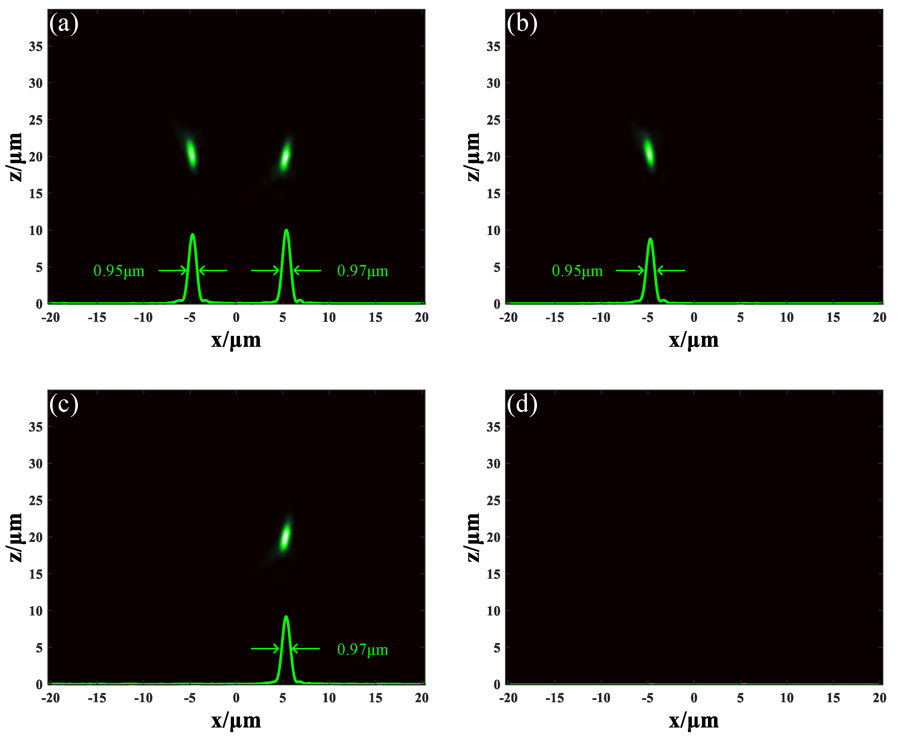
Figure 5.
The light field distribution of metalens M2. (a) The GST in both sections are in amorphous state. (b) The GST in section A stays in amorphous state, but the GST in section B stays in crystalline state. (c) The GST in section A stays in crystalline state, but the GST in section B stays in amorphous state. (d) The GST in both sections are in crystalline state.
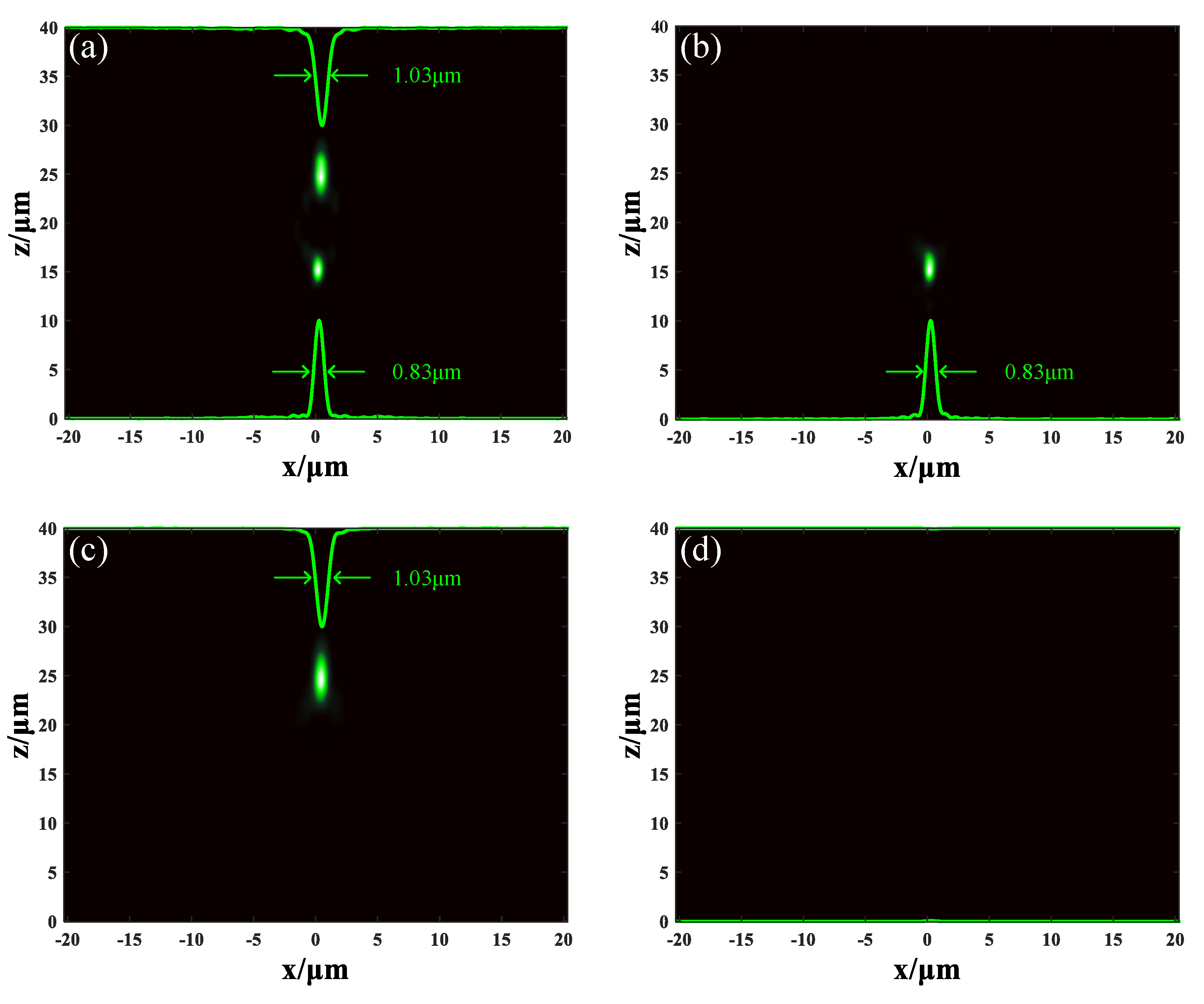
Figure 6.
(a) The conversion efficiency from LCP to RCP versus wavelength for unit cell U2 when GST stays in different states. (b) The phase modulation of unit cell U1 versus rotating angle θ for different states of GST at the designed wavelength of 1.55 μm. (c) The conversion efficiency of unit cell U1 from LCP to RCP versus rotating angle θ for different states of GST at the designed wavelength of 1.55 μm.

Figure 7.
The light field distribution of metalens M3. The red profile and green profile indicate the 1.55 μm and 1.31 μm light respectively. (a) The GST in both sections are in amorphous state. (b) The GST in section A stays in amorphous state but the GST in section B stays in crystalline state. (c) The GST in section A stays in crystalline state but the GST in section B stays in amorphous state. (d) The GST in both sections are in crystalline state.
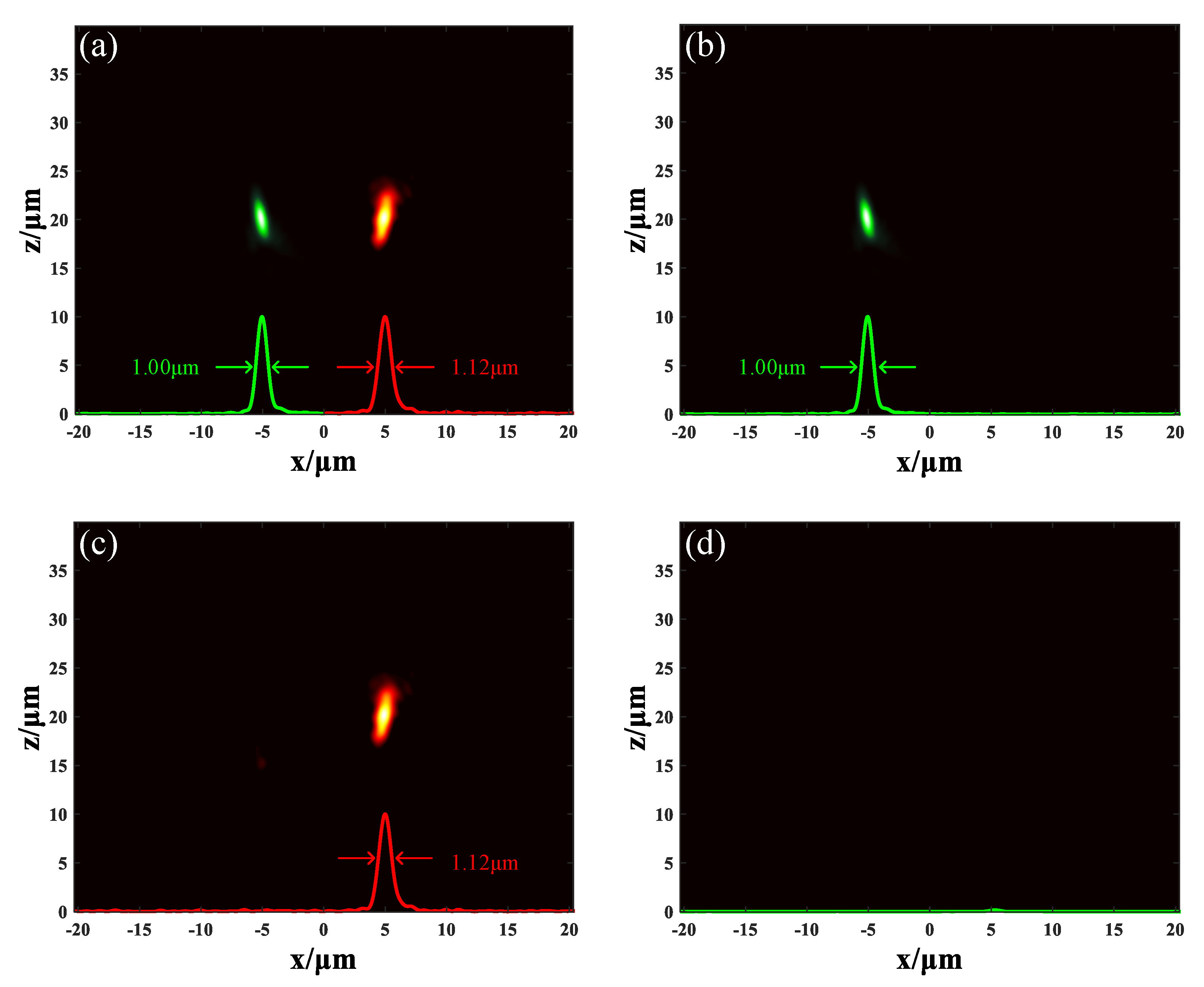
Figure 8.
The light field distribution of metalens M4. (a) The GST in both sections are in amorphous state. (b) The GST in section A stays in amorphous state while the GST in section B stays in crystalline state. (c) The GST in section A stays in crystalline state while the GST in section B stays in amorphous state. (d) The GST in both sections are in crystalline state.


Table 1.
Comparison of the four metalenses.
| Metalens | M1 | M2 | M3 | M4 |
|---|---|---|---|---|
| Constructed unitcell | U1 | U1 | U1 and U2 | U1 and U2 |
| Function | Single-wavelength duplex | Single-wavelength duplex | Dual- wavelength duplex | Dual- wavelength duplex |
| Wavelength | 1.31 μm | 1.31 μm | 1.31 μm and 1.55 μm | 1.31 μm and 1.55 μm |
| Duplex direction | Horizontal | Vertical | Horizontal | Vertical |
| Tunability | Tunable | Tunable | Tunable | tunable |
© 2019 by the authors. Licensee MDPI, Basel, Switzerland. This article is an open access article distributed under the terms and conditions of the Creative Commons Attribution (CC BY) license (http://creativecommons.org/licenses/by/4.0/).
Share and Cite
MDPI and ACS Style
Bai, W.; Yang, P.; Wang, S.; Huang, J.; Chen, D.; Zhang, Z.; Yang, J.; Xu, B. Tunable Duplex Metalens Based on Phase-Change Materials in Communication Range. Nanomaterials 2019, 9, 993. https://doi.org/10.3390/nano9070993
AMA Style
Bai W, Yang P, Wang S, Huang J, Chen D, Zhang Z, Yang J, Xu B. Tunable Duplex Metalens Based on Phase-Change Materials in Communication Range. Nanomaterials. 2019; 9(7):993. https://doi.org/10.3390/nano9070993
Chicago/Turabian StyleBai, Wei, Ping Yang, Shuai Wang, Jie Huang, Dingbo Chen, Zhaojian Zhang, Junbo Yang, and Bing Xu. 2019. "Tunable Duplex Metalens Based on Phase-Change Materials in Communication Range" Nanomaterials 9, no. 7: 993. https://doi.org/10.3390/nano9070993
Note that from the first issue of 2016, this journal uses article numbers instead of page numbers. See further details here.