Characteristics of p-Type Conduction in P-Doped MoS2 by Phosphorous Pentoxide during Chemical Vapor Deposition


Department of Physics and Research Institute of Natural Sciences, Hanyang University, Seoul 04763, Korea
*
Author to whom correspondence should be addressed.
Nanomaterials 2019, 9(9), 1278; https://doi.org/10.3390/nano9091278
Submission received: 19 August 2019
/
Revised: 5 September 2019
/
Accepted: 5 September 2019
/
Published: 7 September 2019
(This article belongs to the Special Issue Preparation and Properties of 2D Materials)
Abstract
:We demonstrated p-type conduction in MoS2 grown with phosphorous pentoxide via chemical vapor deposition (CVD). Monolayer MoS2 with a triangular shape and 15-µm grains was confirmed by atomic force microscopy. The difference between the Raman signals of the A1g and E12g modes for both the pristine and P-doped samples was 19.4 cm−1. In the X-ray photoelectron spectroscopy results, the main core level peaks of P-doped MoS2 downshifted by about 0.5 eV to a lower binding energy compared to the pristine material. Field-effect transistors (FETs) fabricated with the P-doped monolayer MoS2 showed p-type conduction with a field-effect mobility of 0.023 cm2/V⋅s and an on/off current ratio of 103, while FETs with the pristine MoS2 showed n-type behavior with a field-effect mobility of 29.7 cm2/V⋅s and an on/off current ratio of 105. The carriers in the FET channel were identified as holes with a concentration of 1.01 × 1011 cm−2 in P-doped MoS2, while the pristine material had an electron concentration of 6.47 × 1011 cm−2.
1. Introduction
Recently, various studies have analyzed two-dimensional (2D) materials, such as graphene, MoS2, and WSe2, because of their critical properties and abundant potential for use in optical and electrical applications [1,2,3]. Graphene has a zero band gap structure, but has not been able to replace semiconductor-based devices [4,5]. Additionally, layered transition metal dichalcogenides (TMDs) such as MoS2 and WSe2 have received enormous attention as promising materials and layer structures, in which transition metals are sandwiched between two chalcogen atom layers by a covalent force. Moreover, there are Van der Waals (VdW) forces interacting in individual layers, which make exfoliation easily. Interestingly, these materials have a unique property; their band gap structure varies depending on the thickness. In the case of MoS2, the band gap of a monolayer has a direct band gap of 1.8 eV, while a few layers of MoS2 and bulk MoS2 have an indirect band gap structure with a band gap of about 1.2 eV [6].
The chemical vapor deposition (CVD) method has several advantages compared to other methods, such as mechanical and liquid exfoliation methods [7,8]. The disadvantages of the Scotch tape-based mechanical method are its difficulty in controlling the flake thickness, size, and uniformity, which makes it inappropriate for large-scale applications. The liquid method still needs to be developed for applications, while the CVD method has been used to prepare ultrathin monolayers or few-layer MoS2 films over large areas [9]. Transistors have been fabricated via CVD growth of monolayer MoS2. These have been reported to exhibit good properties, including a high on/off current ratio and high mobility [10]. To realize detailed applications, this method needs to be able to produce a junction composed of n- and p-type materials. Although there have been many challenges to p-type doping of MoS2 using niobium (Nb) or phosphorous (P) atoms [11,12], and it remains difficult to successfully dope ultrathin MoS2. According to a previous report, P atoms seem to be the most suitable acceptors among group V elements [13].
In this paper, we report on the CVD growth and characteristics of monolayer MoS2 with and without the addition of phosphorous pentoxide (P2O5) powder. The thickness and grain size of the MoS2 layer were measured using non-contact-mode atomic force microscopy (AFM) and Raman spectroscopy. To confirm the electrical characteristics of MoS2, back-gated field-effect transistors (FETs) were fabricated. The p-type conduction from monolayer MoS2 grown with P2O5 powder was confirmed and compared to pristine MoS2 with n-type behavior.
2. Experimental
To synthesize an MoS2 layer by the CVD method, molybdenum trioxide (MoO3, CERAC Inc, Milwaukee, WI, USA) powder with 99.999% purity as a precursor material and sulfur (iTASCO Inc, Seoul, Korea) powder of 99.999% purity as a reactant material were used. For p-type doping of MoS2 in this experiment, 98.99% purity P2O5 (SIGMA-ALDRICH, St. Louis, MO, USA) powder was added as a dopant material. SiO2/Si substrates (2 × 2 cm2) with a SiO2 thickness of 270 nm and three alumina boats were used. The alumina boats were filled with 10 mg of MoO3 powder, 300 mg of S powder, and 1 mg of P2O5 powder, respectively. During CVD growth of MoS2, the furnace was heated to 750 °C with a heating rate of 30 °C/min under argon gas flowing at 100 sccm. The role of argon gas was to transport S and P2O5 when they were vaporized. During the growth of MoS2, the gas flow and furnace temperature were kept constant for 30 min, and then the furnace was quickly cooled down to room temperature.
The MoS2 thickness and grain size were analyzed by using non-contact-mode atomic force microscopy (AFM) (XE-100, Park’s Systems, Seoul, Korea) and optical microscopy. X-ray photoelectron spectroscopy (XPS) (K-Alpha+, Thermo Fisher Scientific, Waltham, MA, USA) under ~4 × 10⁻¹⁰ Torr and Raman spectroscopy (NRS-3100, JASCO, Tokyo, Japan) with a λ = 532 nm laser were measured at room temperature to identify the doping characteristics. To confirm the electrical characteristics of doped monolayer MoS2, back-gated FETs were fabricated. In this process, photolithography was used for patterning source and drain electrodes of Ni/Au (5 nm/50 nm) metals.
3. Results
Figure 1a shows a simplified schematic diagram for the synthesis of MoS2, with and without phosphorus doping, using the CVD system. Here, MoO3 powder was placed in the middle of the furnace, slightly away from the S and P2O5 powders. The P2O5 powder for P doping was located about 7.5 cm from the MoO3 powder. The ratio of S to Mo atoms is an important point for growing monolayer MoS2 flakes. We used a face-down substrate approach, where the SiO2 substrate is positioned vertically facing the MoO3-containing alumina boat. Unlike previous doping studies that used a two-furnace system [14,15,16], this method used in situ doping with a one-furnace CVD system. The CVD process for MoS2 growth can be divided into two steps: Nucleation and growth. Figure 1b shows the temperature profile of the reaction furnace and pressure variation in the quartz tube with Ar gas flow, respectively, as a function of time. In this figure, S atoms are introduced at 650 °C which is 100 °C lower than the growth temperature (750 °C). When S atoms are introduced, the growth of MoS2 starts and then monolayer MoS2 flakes appear [17].
Figure 2a shows an optical microscopy image of P-doped MoS2 grown via CVD. Here, the MoS2 layers grown on the SiO2/Si substrate under a sufficient S atmosphere were observed to have a triangular shape [17,18]; this is the same shape as pristine MoS2. The grain size of doped MoS2 on the SiO2/Si substrate was about 15 µm. To confirm the formation of a monolayer of P-doped MoS2, Raman spectroscopy and AFM measurements were performed, as shown in Figure 2b,c, respectively. The thickness of an MoS2 flake measured by AFM was about 0.6 nm to 0.9 nm; this layer thickness is the same as a previous result [10]. This measurement value corresponds to the interlayer spacing of a monolayer of S-Mo-S bonding in the MoS2 crystal. Two characteristic Raman peaks, i.e., E12g and A1g from in-plane and out-of-plane modes, respectively, were measured by a laser with an excitation wavelength of 532 nm at room temperature, as shown in Figure 2c. The in-plane E12g mode presents the vibration of one Mo atom and two S atoms in opposite directions, while the out-of-plane A1g mode vibrates only S atoms in opposite directions (as shown in the inset of Figure 2c). From reported results that describe the dependence of the Raman peaks on the number of layers [19,20], we know that the difference between two Raman peaks depending on the number of MoS2 layers is larger than 20 cm−1 for thicknesses above a bilayer (2 L). As shown in Figure 2d, Raman peaks from P-doped MoS2 were located at 384.5 cm−1 (E12g mode) and 403.9 cm−1 (A1g mode). On the other hand, the E12g and A1g signals of the pristine monolayer MoS2 were observed at around 384.6 cm−1 and 405 cm−1, respectively. The difference between the two Raman modes for P-doped and pristine MoS2 (Figure 2d) appear to be about 19.4 cm−1 and 20 cm−1, respectively; these values indicate a single layer of MoS2.
Here, the Raman signal peak of the A1g mode was found to be shifted by about 1.1 cm−1, while the signal peak of the E12g mode was almost unchanged. Azcatl et al. reported that a strain induced by dopants can generate contractions of the MoS2 lattice structure [21]; this phenomenon occurs due to the longer bond length of Mo-S atoms than that of Mo-P atoms. It was also reported that the A1g mode is often more influenced by doping effects than other modes (e.g., the E12g mode); this is due to its strong coupling with electrons [22,23]. Therefore, the Raman active signal with A1g has a shift larger than the other Raman active signal because this peak of the Raman mode is quite sensitive to the doping effect. We confirmed that the Raman shifts in Figure 2d agreed with previous results [24]. The full width at half maximum (FHWM) of the E12g peak was investigated to characterize the crystalline quality of MoS2 obtained by the CVD synthesis method. The FWHM result of the CVD-grown monolayer flake is 3.8 cm−1, which is similar to a recently reported value of a CVD-synthesized single-layer flake [18].
The energy peaks appearing in XPS were also analyzed to confirm the doping properties in monolayer MoS2 crystals. Figure 3a–c show the comparative XPS core level analyses of pristine and doped monolayer MoS2. In Figure 3a, the P 2p binding energy peak, which clearly appears only at 134.3 eV, is associated with a doped flake feature. It is worth mentioning that the existence of this peak provides apparent evidence that P2O5 takes its position before the introduction of S. In addition, the Mo 3d and S 2p core levels indicated that the phenomenon causes a uniform shift of 0.5 eV, from 229.6 eV to 229.1 eV and from 162.4 eV to 161.9 eV, respectively (Figure 3b,c). That is, each peak moved toward a lower binding energy after P-doping, which is very similar to the reported results for Nb-doped MoS2 [24]. This study reported that the Fermi level (EF) of pristine MoS2 is located close to the conduction band (Ec) edge, while an Nb-doped p-type sample has a Fermi level near the valence band edge. The work function and electron affinity of the pristine monolayer MoS2 is 5.1 eV and 4.28 eV, respectively [25]. The pristine MoS2 Fermi level is 0.82 eV, which is the Ec–EF result, and the doping sample Fermi level is 1.32 eV, 0.82 + ΔBE (measured from XPS data). Therefore, it is suggested that doping with P2O5 leads to a downshift in the Fermi level of about 0.5 eV, close to the valence band maximum.
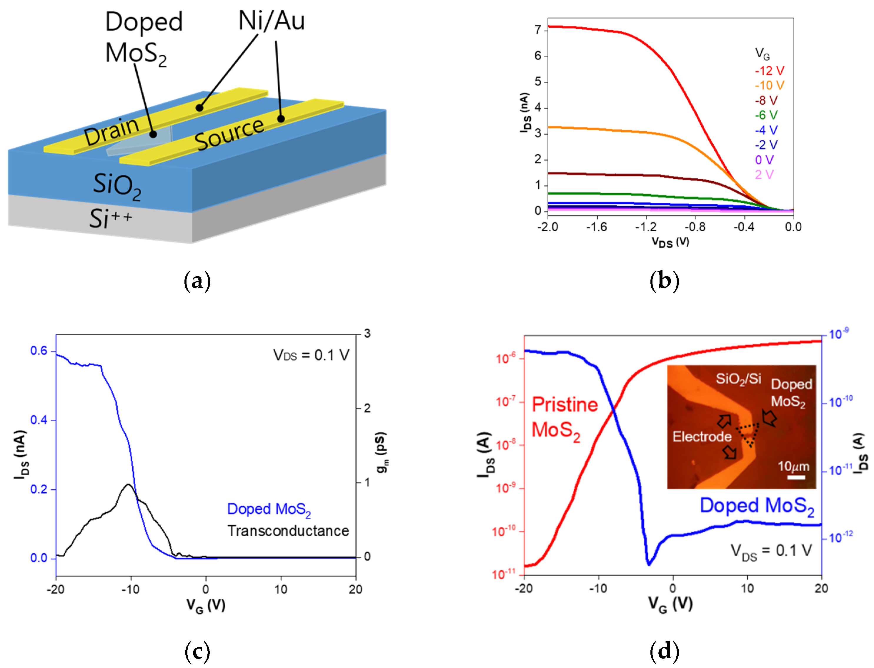
Figure 4a,b show the fabricated back-gate FET schematic with a channel length of 3 µm and a channel width of 10 µm, as well as the IDS–VDS curve of an FET based on P-doped monolayer MoS2, respectively.
Here, Ohmic metals of Ti and Ni were used for n-type pristine and p-type P-doped MoS2 FETs, respectively, to match the metal work functions [26]. Figure 4c shows the transfer characteristics of these devices fabricated on pristine and P-doped monolayer MoS2 flakes. The inset image of Figure 4d is the optical microscopy image of MoS2 FETs which was fabricated on the doped monolayer MoS2. The pristine MoS2 FETs demonstrates n-type conduction with a high on/off current ratio of ~105 [27]. The threshold voltage VT value extracted by the linear extrapolation method was about −8.1 V. In the case of P-doping, the transfer curve indicated p-type conduction with an on/off current ratio of ~103, and the VT was −6.9 V at a drain-source voltage of 0.1 V. The field-effect mobilities of these FETs were calculated by the following relation:
where L and W are the channel length and width, respectively. The back-gate capacitance (Cox = ε0εr/d) was ~1.28 × 10⁻⁸ F/cm2, where ε0X is the dielectric constant and d is the thickness of silicon oxide. Using the transconductance value obtained by the relation of gm = dIDS/dVBG, the field-effect mobilities were determined to be about 29.7 cm2/V⋅s and 0.023 cm2/V⋅s for the pristine and P-doped MoS2 FETs, respectively. The carrier concentration in the FET channel could also be estimated by using the following relation:
where e is the electron charge [28]. The electron concentration in pristine MoS2 was 6.47 × 1011 cm−2, whereas the hole concentration in P-doped MoS2 was 1.01 × 1011 cm−2. Based on these results, the complete p-type conduction of MoS2 with the addition of P2O5 was demonstrated in this study.
µ= (dIDS/dVBG) × [L/Cox WVDS],
n = Cox (VBG − VT)/e,
4. Conclusions
We have demonstrated the p-type conduction of P-doped MoS2 by P2O5 via a CVD process. Based on AFM and Raman measurements, pristine and P-doped MoS2 were confirmed to have monolayer thickness with grain sizes in the order of 15 µm. From XPS data, it was suggested that the Fermi level of P-doped MoS2 shifted by about 0.5 eV toward the valence band compared to the pristine MoS2. FETs with P-doped monolayer MoS2 showed p-type conduction with a field-effect mobility of 0.023 cm2/V⋅s and an on/off current ratio of 103, while pristine MoS2 FETs had n-type behavior with a field-effect mobility of 29.7 cm2/V⋅s and an on/off current ratio of 105. The carriers in the FET channel were identified to be holes with a concentration of 1.01 × 1011 cm−2 in P-doped MoS2 and electrons with a concentration of 6.47 × 1011 cm−2 in the pristine material. This phosphorous doping technique should be applicable to other TMD materials.
Author Contributions
J.S.L. performed the experiment, data analysis, discussed the results and wrote the paper; C.-S.P., T.Y.K. and Y.S.K. discussed the results and analyzed the data; and E.K.K. performed paper editing and supervision.
Funding
This research was supported by a National Research Foundation of Korea (NRF) grant funded by the Korean government (MSIP) (NRF-2016R1A2B4011706, NRF-2018R1A2A3074921).
Conflicts of Interest
The authors declare no conflict of interest.
References
- Novoselov, K.S.; Geim, A.K.; Morozov, S.V.; Jiang, D.; Zhang, Y.; Dubonos, S.V.; Griorieva, I.V.; Firsov, A.A. Electric field effect in atomically thin carbon films. Science 2004, 306, 666–669. [Google Scholar] [CrossRef] [PubMed]
- Bolotin, K.I.; Sikes, K.J.; Jiang, Z.; Klima, M.; Fudenberg, G.; Hon, J.; Kim, P.; Stormer, H.L. Ultrahigh electron mobility in suspended graphene. Solid State Commun. 2008, 146, 351–355. [Google Scholar] [CrossRef] [Green Version]
- Liu, M.; Yin, X.; Ulin-Avila, E.; Geng, B.; Zentgraf, T.; Ju, L.; Wang, F.; Zhang, X. A graphene based broadband optical modulator. Nature 2011, 474, 64–67. [Google Scholar] [CrossRef] [PubMed]
- Ozlem, S.; Akkaya, U. Graphene electronics: Thinking outside the silicon box. Nat. Nanotechnol. 2009, 131, 48–49. [Google Scholar]
- Osada, M.; Sasaki, T. 2D inorganic nano-sheets: Two-dimensional dielectric nano-sheets: Novel nanoelectronics from nanocrystal building blocks. Adv. Mater. 2012, 24, 210–228. [Google Scholar] [CrossRef] [PubMed]
- Gordon, R.; Yang, D.; Crozier, E.; Jiang, D.; Frindt, R. Structures of exfoliated single layers of WS2, MoS2, and MoSe2 in aqueous suspension. Phys. Rev. B 2002, 65, 125407. [Google Scholar] [CrossRef]
- Chu, D.; Pak, S.W.; Kim, E.K. Locally Gated SnS2/hBN Thin Film Transistors with a Broadband Photoresponse. Sci. Rep. 2018, 8, 10585–10593. [Google Scholar] [CrossRef] [PubMed]
- Lee, S.K.; Chu, D.; Yoo, J.; Kim, E.K. Formation of transition metal dichalcogenides thin films with liquid phase exfoliation technique and photovoltaic applications. Sol. Energy Mater. Sol. Cells 2018, 184, 9–14. [Google Scholar] [CrossRef]
- Qiu, D.; Lee, D.U.; Pak, S.W.; Kim, E.K. Structural and optical properties of MoS2 layers grown by successive two-step chemical vapor deposition method. Thin Solid Films 2015, 587, 47–51. [Google Scholar] [CrossRef]
- Radisavljevic, B.; Radenovic, A.; Brivio, J.; Giacometti, V.; Kis, A. Single-layer MoS2 transistors. Nat. Nanotechnol. 2011, 6, 147–150. [Google Scholar] [CrossRef]
- Laskar, M.R.; Nath, D.N.; Ma, L.; Lee, E.W.; Lee, C.H.; Kent, T.; Yang, Z.; Mishra, R.; Roldan, M.A.; Idrobo, J.-C.; et al. p-type doping of MoS2 thin films using Nb. Appl. Phys. Lett. 2014, 104, 092104. [Google Scholar] [CrossRef]
- Momose, T.; Nakamura, A.; Daniel, M.; Shimomura, M. Phosphorous doped p-type MoS2 polycrystalline thin films via direct sulfurization of Mo film. AIP Adv. 2018, 8, 025009. [Google Scholar] [CrossRef]
- Dolui, K.; Rungger, I.; Pemmaraju, C.D.; Sanvito, S. Possible doping strategies for MoS2 monolayers: Anab initiostudy. Phys. Rev. B 2013, 88, 075429. [Google Scholar] [CrossRef]
- Xu, E.Z.; Liu, H.M.; Park, K.; Li, Z.; Losovyj, Y.; Starr, M.; Werbianskyj, M.; Fertig, H.A.; Zhang, S.X. p-Type transition-metal doping of large-area MoS2 thin films grown by chemical vapor deposition. Nanoscale 2017, 9, 3576–3584. [Google Scholar] [CrossRef] [PubMed]
- Zhang, K.; Bersch, B.M.; Joshi, J.; Addou, R.; Cormier, C.R.; Zhang, C.; Xu, K.; Briggs, N.C.; Wang, K.; Subramanian, S.; et al. Tuning the Electronic and Photonic Properties of Monolayer MoS2 via In Situ Rhenium Substitutional Doping. Adv. Funct. Mater. 2018, 28, 1706950. [Google Scholar] [CrossRef]
- Zhang, K.; Feng, S.; Wang, J.; Azcatl, A.; Lu, N.; Addou, R.; Wang, N.; Zhou, C.; Lerach, J.; Bojan, V.; et al. Manganese Doping of Monolayer MoS2: The Substrate Is Critical. Nano Lett. 2015, 15, 6586–6591. [Google Scholar] [CrossRef]
- Xie, Y.; Wang, Z.; Zhan, Y.; Zhang, P.; Wu, R.; Jiang, T.; Wu, S.; Wang, H.; Zhao, Y.; Nan, T.; et al. Controllable growth of monolayer MoS2 by chemical vapor deposition via close MoO2 precursor for electrical and optical applications. Nanotechnology 2017, 28, 084001. [Google Scholar] [CrossRef]
- Wang, S.; Rong, Y.; Fan, Y.; Pacios, M.; Bhaskaran, H.; He, K.; Warner, J.H. Shape Evolution of Monolayer MoS2 Crystals Grown by Chemical Vapor Deposition. Chem. Mater. 2014, 26, 6371–6379. [Google Scholar] [CrossRef]
- Li, H.; Zhang, Q.; Yap, C.C.R.; Tay, B.K.; Edwin, T.H.T.; Olivier, A.; Baillargeat, D. From Bulk to Monolayer MoS2: Evolution of Raman Scattering. Adv. Funct. Mater. 2012, 22, 1385–1390. [Google Scholar] [CrossRef]
- Lee, C.G.; Yan, H.; Brus, L.E.; Heinz, T.F.; Hone, J.; Ryu, S. Anomalous Lattice Vibrations of Single-and Few-Layer MoS2. ACS Nano 2010, 4, 2695–2700. [Google Scholar] [CrossRef]
- Azcatl, A.; Qin, X.; Prakash, A.; Zhang, C.; Cheng, L.; Wang, Q.; Lu, N.; Kim, M.J.; Kim, J.; Cho, K.; et al. Covalent Nitrogen Doping and Compressive Strain in MoS2 by Remote N2 Plasma Exposure. Nano Lett. 2016, 16, 5437–5443. [Google Scholar] [CrossRef] [PubMed]
- Chakraborty, A.; Bera, A.; Muthu, D.V.S.; Bhowmick, S.; Waghmare, U.V.; Sood, A.K. Symmetry-dependent phonon renormalization in monolayer MoS2 transistor. Phys. Rev. B 2012, 85, 161403. [Google Scholar] [CrossRef]
- Kukucska, G.; Koltai, J. Theoretical Investigation of Strain and Doping on the Raman Spectra of Monolayer MoS2. Phys. Status Solidi (B) 2017, 254, 1700184. [Google Scholar] [CrossRef]
- Suh, J.; Park, T.E.; Lin, D.Y.; Fu, D.; Park, J.; Jung, H.J.; Chen, Y.; Ko, C.; Jang, C.; Sun, Y.; et al. Doping against the native propensity of MoS2: Degenerate hole doping by cation substitution. Nano Lett. 2014, 14, 6976–6982. [Google Scholar] [CrossRef] [PubMed]
- Velicky, M.; Bissett, M.A.; Woods, C.R.; Toth, P.S.; Georgiou, T.; Kinloch, I.A.; Novoselov, K.S.; Dryfe, R.A. Photoelectrochemistry of Pristine Mono- and Few-Layer MoS2. Nano Lett. 2016, 16, 2023–2032. [Google Scholar] [CrossRef] [PubMed]
- McDonnell, S.; Addou, R.; Buie, C.; Wallace, R.M.; Hinkle, C.L. Defect-Dominated Doping and Contact Resistance in MoS2. ACS Nano 2014, 8, 2880–2888. [Google Scholar] [CrossRef] [PubMed]
- Zhang, Y.; Li, H.; Wang, H.; Xie, H.; Liu, R.; Zhang, S.L.; Qiu, Z.J. Thickness Considerations of Two-Dimensional Layered Semiconductors for Transistor Applications. Sci. Rep. 2016, 6, 29615–29622. [Google Scholar] [CrossRef] [PubMed]
- Zhang, S.; Hill, H.M.; Moudgil, K.; Richter, C.A.; Walker, A.R.H.; Barlow, S.; Marder, S.R.; Hacker, C.A.; Pookpanratana, S.J. Controllable, Wide-Ranging n-Doping and p-Doping of Monolayer Group 6 Transition-Metal Disulfides and Diselenides. Adv. Mater. 2018, 30, 1802991–1802999. [Google Scholar] [CrossRef] [PubMed]
Figure 1.
(a) Schematic diagram of the chemical vapor deposition (CVD) process for the monolayer MoS2 synthesis and in situ P doping with P2O5 powder. (b) Temperature profile of the reaction furnace and pressure in the quartz tube as a function of the processing time.
Figure 1.
(a) Schematic diagram of the chemical vapor deposition (CVD) process for the monolayer MoS2 synthesis and in situ P doping with P2O5 powder. (b) Temperature profile of the reaction furnace and pressure in the quartz tube as a function of the processing time.
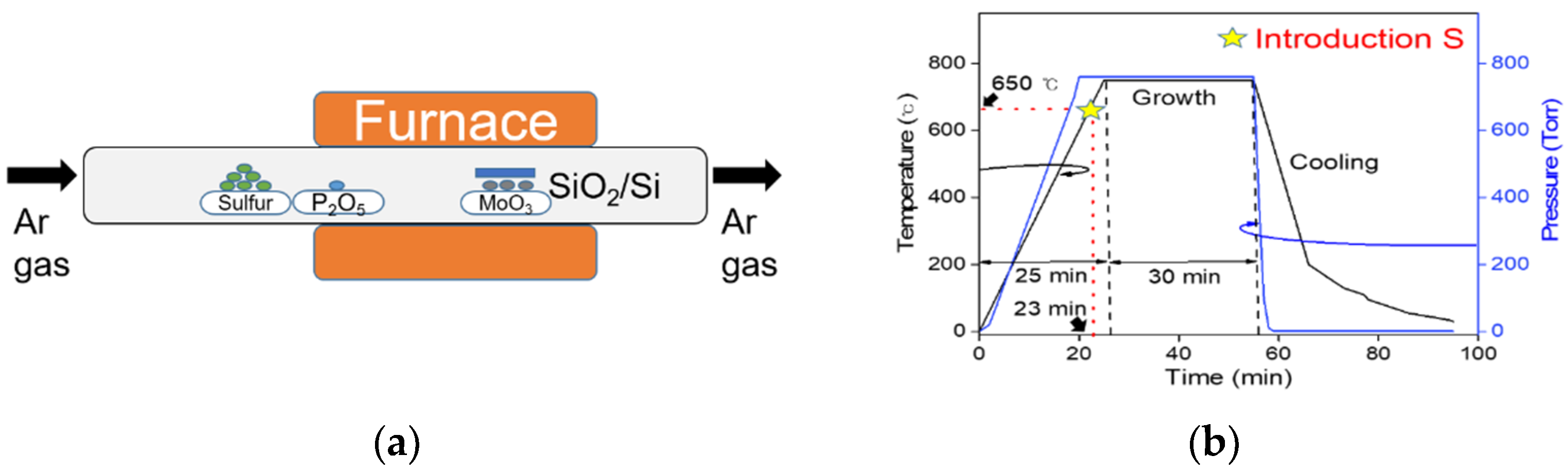
Figure 2.
(a) Optical microscope image, (b) AFM height profile, and (c) Raman spectroscopy results using a laser with an excitation wavelength of 532 nm for a monolayer of CVD-grown MoS2 flakes. (d) The two Raman modes for the pristine and doped monolayer MoS2 flakes.
Figure 2.
(a) Optical microscope image, (b) AFM height profile, and (c) Raman spectroscopy results using a laser with an excitation wavelength of 532 nm for a monolayer of CVD-grown MoS2 flakes. (d) The two Raman modes for the pristine and doped monolayer MoS2 flakes.
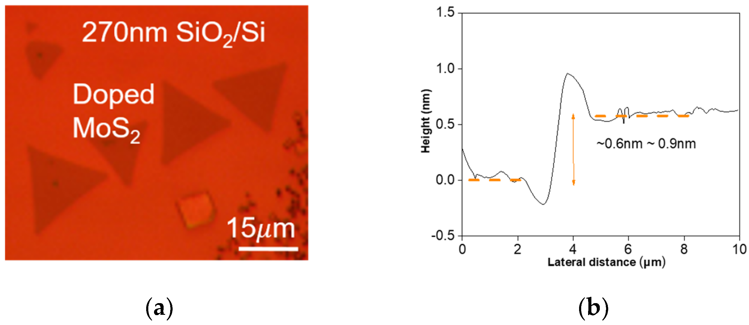

Figure 3.
XPS spectra of (a) P 2p, (b) Mo 3d, and (c) S 2p peaks in the pristine and doped MoS2. These results indicate that the peaks of each core level are downshifted in the doped MoS2 flake.
Figure 3.
XPS spectra of (a) P 2p, (b) Mo 3d, and (c) S 2p peaks in the pristine and doped MoS2. These results indicate that the peaks of each core level are downshifted in the doped MoS2 flake.

Figure 4.
(a) Schematic of field-effect transistors (FETs) with a channel length of 3 nm and a channel width of 10 nm. (b) IDS–VDS curves of a P-doped monolayer MoS2 FET with different gate voltages. (c,d) Linear and log scales of the transfer characteristics as a function of the gate voltage for FETs with pristine and P-doped MoS2 channels, respectively.
© 2019 by the authors. Licensee MDPI, Basel, Switzerland. This article is an open access article distributed under the terms and conditions of the Creative Commons Attribution (CC BY) license (http://creativecommons.org/licenses/by/4.0/).
Share and Cite
MDPI and ACS Style
Lee, J.S.; Park, C.-S.; Kim, T.Y.; Kim, Y.S.; Kim, E.K. Characteristics of p-Type Conduction in P-Doped MoS2 by Phosphorous Pentoxide during Chemical Vapor Deposition. Nanomaterials 2019, 9, 1278. https://doi.org/10.3390/nano9091278
AMA Style
Lee JS, Park C-S, Kim TY, Kim YS, Kim EK. Characteristics of p-Type Conduction in P-Doped MoS2 by Phosphorous Pentoxide during Chemical Vapor Deposition. Nanomaterials. 2019; 9(9):1278. https://doi.org/10.3390/nano9091278
Chicago/Turabian StyleLee, Jae Sang, Chang-Soo Park, Tae Young Kim, Yoon Sok Kim, and Eun Kyu Kim. 2019. "Characteristics of p-Type Conduction in P-Doped MoS2 by Phosphorous Pentoxide during Chemical Vapor Deposition" Nanomaterials 9, no. 9: 1278. https://doi.org/10.3390/nano9091278
Note that from the first issue of 2016, this journal uses article numbers instead of page numbers. See further details here.