Article

Graphene Synthesis by Inductively Heated Copper Foils: Reactor Design and Operation

1
Laboratoire des Sciences des Procédés et des Matériaux, Université Sorbonne Paris Nord, CNRS, LSPM-UPR 3407, F-93430 Villetaneuse, France
2
Department of Chemical Engineering, University of Chemical Technology and Metallurgy, 8 Boulevard St. Kliment Ohridski, 1756 Sofia, Bulgaria
3
Laboratoire Matériaux, Molécules et Applications (Amilcar), Institut Préparatoire aux études scientifiques et techniques (IPEST), Université de Carthage, La Marsa 2070, Tunisia
*
Author to whom correspondence should be addressed.
Coatings 2020, 10(4), 305; https://doi.org/10.3390/coatings10040305
Submission received: 12 February 2020 / Revised: 19 March 2020 / Accepted: 23 March 2020 / Published: 25 March 2020
(This article belongs to the Special Issue Advances in Flexible Films and Coatings)

Abstract

:
We report on the design of a reactor to grow graphene via inductively heating of copper foils by radio frequency (RF) magnetic fields. A nearly uniform magnetic field induced by Helmholtz-like coils penetrates the copper foil generating eddy currents. While the frequency of the current is being rapidly varied, the substrate temperature increases from room temperature to ~1050 °C in 60 s. This temperature is maintained under Ar/H2 flow to reduce the copper, and under Ar/H2/CH4 to nucleate and grow the graphene over the entire copper foil. After the power cut-off, the temperature decreases rapidly to room temperature, stopping graphene secondary nucleation. Good quality graphene was obtained and transferred onto silicon, and coated with a 300 nm layer of SiO2 by chemical etching of the copper foil. After synthesis, samples were characterized by Raman spectroscopy. The design of the coils and the total power requirements for the graphene induction heating system were first estimated. Then, the effect of the process parameters on the temperature distribution in the copper foil was performed by solving the transient and steady-state coupled electromagnetic and thermal problem in the 2D domain. The quantitative effects of these process parameters were investigated, and the optimization analysis results are reported providing a root toward a scalable process for large-sized graphene.

1. Introduction

Due to its impressive conjunction of optical, mechanical, and electrical properties, graphene is a strategic material in flexible film technology including, but not limited to, next-generation flexible electronics [1,2,3,4,5], where high transparency and ultrasensitive responses properties could be insured by single-layer graphene films. Nevertheless, there are still several challenges to produce graphene of high enough quality to be commercially viable. To date, it is suggested that the formation of graphene is governed by the kinetics of nucleation and growth, but the nature of growth precursors is still unclear. Should we decompose the gaseous precursor, such as methane, by heating the gas in the volume? Or can the catalyst directly make this decomposition without being necessary to heat the overall surrounding gas? Thus, the activation of the system by thermal, plasma, or inductive heating has a direct impact on nucleation and growth kinetics. When heated close to its melting point of 1084 °C, copper ensures a low-energy pathway by forming intermediate carbon compounds from hydrogen and hydrocarbon precursors. Activated carbon formed from the adsorbed hydrocarbon induces graphene nucleation, which is the result of competition between the rates of nucleus growth by adatom capture, the surface diffusion of carbon species and desorption of carbon adatoms, and graphene growth by attachment of active carbon species onto the graphene edge. During the chemical vapor deposition (CVD) process, Vlassiouk et al. [6] estimated the activation energy for graphene nucleation on copper at 4 eV at low pressure CVD of 5 Torr. Higher activation energy of 9 eV is needed at atmospheric pressure CVD. As the nucleation and growth of graphene are thermally activated processes, the surface temperature plays a predominant role. Indeed, temperature affects the nucleation density of graphene, thereby determining the graphene domain sizes that in turn will grow by adding precursors to their edges until covering the entire copper surface. Therefore, the final size of domains, together with interconnections between them, influences the final graphene properties [7]. However, for defect-free large single-crystal graphene synthesis, it is necessary to carefully control the substrate temperature for quite a long time. In thermal CVD, heat energy is supplied to activate the required gas and gas–solid phase reactions through ovens in hot-wall reactors. For large-scale processing, as rate processes are scale-dependent, heating larger copper substrates necessitates larger ovens with huge volumes. Despite technological advances in multi-zone furnaces with multiple independently controlled zones, temperature gradient control becomes more difficult for a longer heating zone. The same reasoning could apply in the case of large-sized substrate processing by plasma activation, where scaling up would generate higher plasma power coupling for higher ionization efficiency in order to sustain stable plasma over a large volume. This makes thermal CVD and plasma-enhanced CVD (PECVD) less energy efficient as the system size is increased.
An alternative CVD method in which the growth is performed in a cold wall CVD system is the contactless heating method that combines electrical, magnetic, and thermal phenomena, where only the thin copper foil is heated. Due to its advantages regarding efficiency, fast heating, and accurate control, inductive heating has been commonly used in industry for metal treatment applications including surface hardening, melting and sealing. As compared to hot-wall CVD reactors, the advantages of the induction heating are that the metal may be directly heated, without the need to heat the surrounding gas and there is no contact between the heat source and the substrate. Therefore, in inductive heating, the reactor walls remain cool, limiting the thermal breakdown of reactant gases. Furthermore, the fact that heating is done without contact limits any contamination by pyrolytic carbon deposition from graphite resistor generally used in substrate holder for resistive heating.
The inductive heating CVD method has been used previously for growing graphene [8,9,10] and carbon nanotubes [11]. Sosnowchik et al. [11] proposed an inductive heating method for the synthesis of carbon nanotubes (CNTs) in a room temperature environment. The complete synthesis time was less than 2 min, and the growth rate of CNTs was as high as 200 μm/min. Piner et al. [8] used magnetic inductive heating for high-quality graphene films synthesis on 125 μm thick oxygen-free copper foil. The substrate was heated directly by the RF field, which allows rapid temperature ramp of typically 30 °C/s. The synthesized graphene was of quality comparable or higher than the other CVD methods. Seifert et al. [9] demonstrated a time-effective CVD process for the growth of high-quality graphene layers on millimeter-thick Cu and Pt substrates via induction heating. Based on a detailed parametric study for the CVD growth, a two-step growth process was established and the resulting graphene domain size was approximately 90 μm. Wu et al. [10] proposed a method based on electromagnetic induction heating for controlled formation of single-crystal graphene. Direct observation of the graphene growth was performed. They were able to observe the growth kinetics by rapidly terminating the graphene growth. Therefore, predicting eddy currents and temperature, as well as their spatial distribution in the copper foil, are the major parameters to be determined during graphene growth. In addition, understanding the physics of induction in the graphene growth context is quite crucial when designing a new reactor.
In this paper, we propose a detailed design of a reactor for graphene growth on RF-heated copper substrates. The reactor is composed of two concentric quartz tubes placed between RF induction coil in Helmholtz configuration fed by a power supply of high-frequency alternating current and cooled by a chiller. The inner quartz tube serves as a support for the copper foil. First, a simple model is used to estimate the total power requirements for the induction heating systems by solving the heat balance between the heat absorbed from the electromagnetic field and lost by radiation and convection in the (0D) spatial dimension. Then, a two-dimensional (2D) transient mathematical model for the induction heating process is proposed to design the reactor with the RF-heated copper foil. This approach allows investigating the effects of transient heating and cooling as well determining the temperature distribution within the copper foil. Finally, the reactor is used to grow graphene under specific conditions. The structural properties of the obtained graphene are investigated using Raman spectroscopy and corroborated by scanning electron microscope (SEM) to study the early graphene nucleation step. The obtained graphene from the RF-heated copper is of good quality, comparable to CVD graphene, with several advantages as reduced growth time and the absence of any contact between the substrate and the heating source, thereby limiting graphene contamination. In addition, the reactor concept, as well as the design methodology proposed in this paper, could be used for scale-up purpose and easily adapted to other catalysts, such as cobalt, nickel, or molybdenum, and other 2D materials.

2. Reactor Design

To generate a uniform electromagnetic field we used circular coils in the Helmholtz configuration. As compared to a solenoid coil, the variation in field strength between the center and the planes of the coils could be adjusted by an appropriate choice of the distance (H) between the coils and the copper substrate placed at the geometric center of the Helmholtz set-up. If this distance is equivalent to the radius of the circular loops (R), the difference in the magnetic field between the center and the planes of the coils is reduced, thereby improving the field’s uniformity in the region near the center of the substrate. Consequently, a more uniform temperature distribution on the substrate could be created, allowing the same graphene growth from the precursors across the sample. As the control of the temperature is a critical factor in scaling graphene growth for industrial applications, RF heating is a useful tool. Figure 1a shows a representation of the Helmholtz coils specially designed for our inductive heating set and manufactured by Ambrell Ltd. The reversal of the tubes at the support allows the connection of the coils to the heat exchanger. This does not interfere with the current loops at the coils which could be represented simply by circular coils in the same plane as schematically shown in Figure 1b,c. In the case of Helmholtz configuration, the magnetic field is perpendicular to the substrate and the electric field is in the substrate plane as shown in Figure 1d.
The electromagnetic field generated by a circular wire loop carrying current will satisfy the Maxwell equations. For a coil comprising N circular turns of radius R excited with low-frequency current I, almost all the energy is stored in the magnetic field. Determining the uniformity of the magnetic field involves integral calculations. In the case of contiguous turns, the magnetic field generated by the coils on a radial position (x) shown in Figure 1c is given by the following equation,
Bz   ( x ) = N × I × μ 0 4 π 0 2 π 2 R ( R xcos ( θ ) ) d θ ( R 2 + H 2 + x 2 2 R   x   cos ( θ ) ) 3 / 2   ,
where R is the radius of the coils [m], H is the distance to the median plane of the coil and the substrate [m], B is the magnetic field at the median plane [T], θ is the angle between the median plane and the B field [rad], x is the radial position, N is the number of turns of each coil, and I is the current flowing through the turns. For non-contiguous loops centered at axial positions, Q, the magnetic field is derived from the Biot–Savart equation:
B ( N ) = μ 0 4 π Q 0 2 π I R d θ t × P N / ( P N ) 3 ,
where
t = s i n θ u x + c o s θ u y   and   P N = ( x R c o s θ ) u x + ( R s i n θ ) u y + ( z z P ) u z
For N on the z axis, the magnetic field is parallel to the z axis and its magnitude reads
B = μ 0 2 Q R 2 / ( R 2 + ( z z Q ) 2 ) 3 ,
In the case where R = H, and assuming contiguous turns, an almost uniform field B is established, which is given by the following relation,
B = μ0 N I R2/(R2 + H2)3/2,
and the power QB (Watt) provided to the coil is
QB = 2N π R2 B ω I,
where μ0 is the permeability of free space (4 π × 10 −7 H·m−1) and ω = 2 π f is the angular frequency (Hz) with f being the frequency (Hz). Induction heating occurs due to electromagnetic force fields producing an electrical current in the copper substrate. The magnetic field exerts a force on the free electrons present in the copper, thus generating an electric current. The energy then dissipates inside the copper in the form of heat, depending on the electrical conductivity of the material and its skin depth. The skin depth δ [m] of a material determines, as a first approximation, the width of the material where ~86% of the power will be concentrated in the surface layer [12]. As shown in Equation (6), by applying a high-frequency, alternating current through the induction coil, the skin depth δ can be small enough to allow effective Joule heating to occur in thin substrates, but if δ is larger than the thickness of the substrate, it may be difficult to heat inductively [11].
δ = 1 σ   μ   π   f ,
where f is the frequency of the current [Hz], μ is the magnetic permeability [H/m], and σ is the electrical conductivity [S/m] obtained from the resistivity, noticed ρ.
σ = 1 ρ ,
According to Bloch–Grüneisen model, electron–phonon resistivity depends on the temperature. For good electrical conductors as copper, the temperature dependence of the electrical resistivity ρ(T) due to the scattering of electrons by acoustic phonons changes from a high-temperature regime, in which ρ ∝ T, to a low-temperature regime, in which ρ ∝ T5. The transition between these two regimes occurs at the Debye temperature θD = 347 K for copper [13]. Therefore, the temperature dependence of resistivity is represented by the empirical relationship
ρ = ρ 0 ( 1 + α T ) ,
where ρ0 is the resistivity at a reference temperature, usually room temperature, and α is the temperature coefficient. For annealed copper at room temperature, ρ0 = 1.7241 × 10⁻⁸ Ω·m, α = 0.0039 K−1, and the magnetic permeability μ = 1.256629 × 10⁻⁶ H/m [14]. To maintain the RF coil current at a desired set point, the frequency must be automatically adjusted in the range of 200 to 250 kHz. Therefore, we calculated the copper skin depth in this frequency range at room temperature of 20 °C and at the average graphene growth temperature using Equations (6)–(8), i.e., 1035 °C. Figure 2 shows the effect of temperature and frequency on copper skin depth. At higher frequencies and lower temperatures, the skin depth is smaller. The calculated average skin depth of copper is 204 μm at room temperature and 344 μm at 1035 °C. As the copper foil dissolves during the transfer of graphene, it is advisable to minimize its thickness to reduce the dissolution time. Nevertheless, as discussed by Piner et al., reducing copper foils down to 25 μm induces “hot-spots”, leading fatally to substrate melting. This makes the control of the power difficult to maintain the temperature at the desired value. Increasing foil thickness below the skin depth improves the RF coupling efficiency and ensures thermal stability and uniformity [8]. Therefore, we found that 125 μm thickness is a good trade-off in choosing the copper foil.
Given the skin depth δ, the substrate radius r(m), and the frequency ω, the net absorbed power by the substrate QA(Watt) could be estimated from the magnetic field by
QA = B2 ω2 (σ/2) π (r4/4) δ,
Using this simple model, we can easily estimate, in a preliminary way, the power of the generator necessary to heat a copper substrate to the average graphene growth temperature of ~1050 °C. For these calculations, we fixed the geometrical parameters N=2, the coil radius R = 1.81 × 10⁻² m, and the distance between the coils H = 1.81 × 10⁻² m. Then, the substrate radius was chosen at its maximum value r = 1.5 × 10⁻² m and the copper thickness at δ = 125 μm. The net absorbed power QA by the copper foil is evacuated by convection and radiation through the thin copper foil surface area of radius r. Assuming the actual temperature of the copper foil as T, the ambient temperature as T0, the average convective heat transfer coefficient h (W.m−2.K−1), the Stefan–Boltzmann constant σSF = 5.67 × 10⁻⁸ W m−2K−4, and the copper emissivity of ε:
QA = B2 ω2 (σ/2) π (r4/4) δ = 2 π r2 [h (T − T0) + ε σSF (T4 − T04)],
Solving the algebraic fourth-order Equation (10) leads to the substrate temperature for a given current I. The convective heat transfer coefficient h could be estimated from the Nusselt number (Nu), given the thermal conductivity of the fluid λ and a characteristic length L of the copper foil,
h = Nu λ/L,
In the steady flow regime, the Nusselt number is calculated for an isothermal flat plate in the free stream as a function of dimensionless Reynolds (Re) and Prandtl (Pr) numbers. Therefore, empirical correlations could be used to estimate Nu from fluid properties Re = ρ v L/μ and Pr = cp μ/λ, where v(m·s−1) is the fluid velocity, and μ(N·s·m−2), cp(J·kg−1K−1), ρ(kg·m−3), and λ(W·m−1K−1) are the fluid dynamic viscosity, specific heat, density, and thermal conductivity, respectively [15,16].
Nu = 0.664 Re0.5 Pr0.33 for laminar flow with Re < 500,000,
For a given flowrate flowing in a reactor of 2.5 × 10⁻² m inner diameter, we can estimate the fluid velocity and properties at an average fluid temperature Tf = (T + T0)/2. Table 1 summarizes the data used for seven variants of the process. The first five conditions show the effect of the surrounding gas nature and flow rate on convective heat transfer, whereas conditions 6 and 7 represent the steps for copper reduction under Ar/H2 and graphene nucleation and growth occurring under Ar/H2/CH
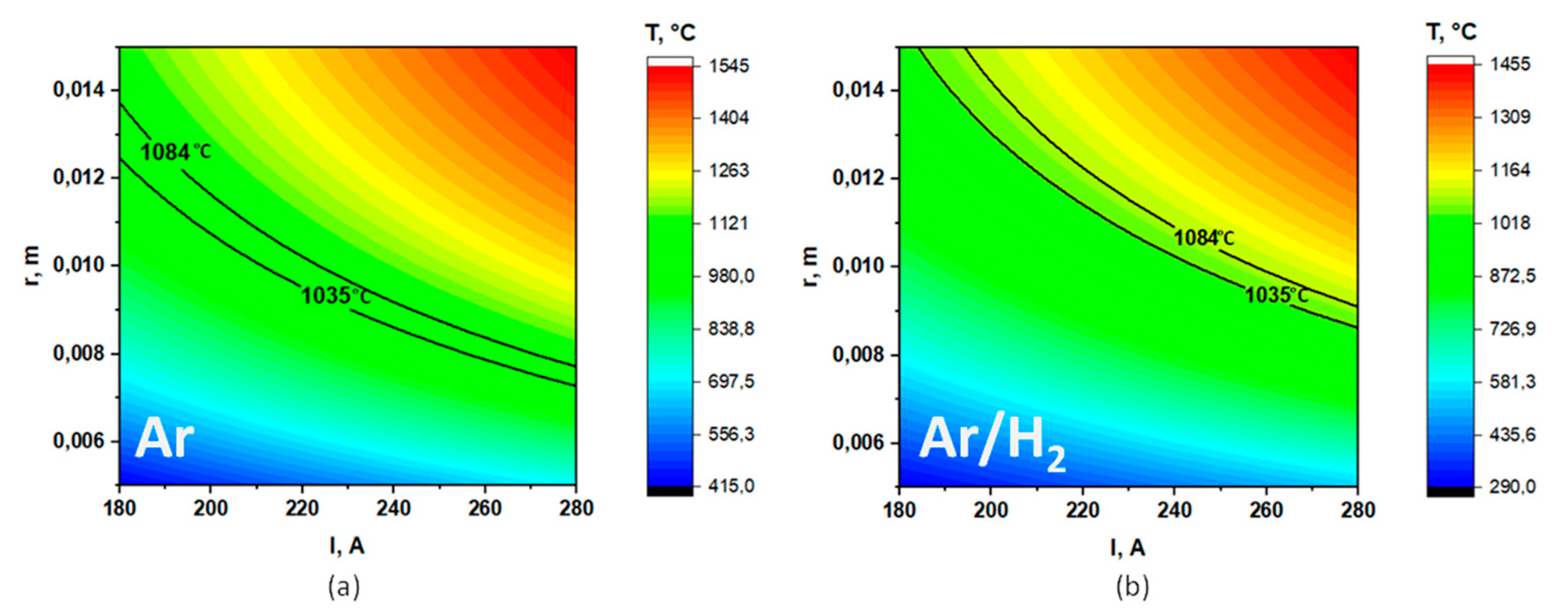
4, respectively. For all these calculations, we fixed the total pressure at 150 mbar, substrate temperature T = 1308 K (1035 °C), ambient temperature T0 = 300 K, and average fluid temperature Tf = 803 K.
From the calculations of Table 1, it is evident that the convective heat transfer coefficient depends on the surrounding gas. For the same flowrate of 500 sccm, convective heat transfer coefficients are in this order hH2 > hCH4 > hAr (conditions 1 to 3 in Table 1). As depicted by Figure 3, adding hydrogen and/or methane to the argon increases h. In these conditions, when changing the gases required for the thermal annealing and/or nucleation and growth of graphene, the current in the turns must be adjusted to maintain a given temperature on the substrate.
For an average frequency of ω = 220 kHz, we calculated the electrical current needed to maintain the substrate temperature at 1050 °C by solving Equation (10). Note that radiative heat losses depend on copper emissivity, which is sensitive to the surface state. Indeed, surface emissivity refers to the efficiency in which the surface emits thermal energy. For the polished copper foil, ε = 0.05 at ambient temperature and ε = 0.16 at 1077 °C. However, surface emissivity could be influenced by the graphene deposited on the top. To the best of the authors’ knowledge, no experimental data are available for graphene/copper emissivity. Recently, Zhao et al. measured infrared emissivity of ε = 0.41 to 0.57 from the surface of multilayer graphene on polished copper after ionic liquid intercalation [17]. To scale-up the generator we assumed an emissivity of ε = 1 and we considered h = 7.1 × W m−2 K−1. In these conditions, a current of I = 77.4 A is necessary to maintain the substrate temperature at 1050 °C. The calculated magnetic field intensity is B = 38 Gauss, the net absorbed power by the substrate QA = 257 W and the power to be supplied to the 2N coils QB = 1674 W. As the generator must be able to generate a power of ~2 kW, we scaled it up to 2.4 kW. The low magnetic field suggests that it is not necessary to equip the device with a Faraday cage. In addition, since the generator controls the current by adjusting the frequency when injecting methane to the hydrogen/argon mixture, electrical current I is increased to maintain the desired substrate temperature. Finally, to derive the magnetic field at any position, we numerically calculate the integral of Equation (2). According to the Biot–Savart–Laplace law, the resulting field of the coils is equal to the vector sum of the fields generated by each coil.
Figure 4a,b shows the magnetic field distribution and its relative uniformity on the z-axis respectively. As uniform magnetic field is required for good heating uniformity, the magnetic field axial relative uniformity noticed δz, was estimated from the relation
δ z = B z ( z , 0 ) B z ( 0 , 0 )   B z ( 0 , 0 ) ,
where Bz(0,0) is the magnetic field at the geometric center of the Helmholtz coils [18].
The magnetic field axial uniformity δz of 10 % can be obtained at a distance from the geometric center z ≤ 5.35 mm (shown by the broken line in Figure 5b). By analogy, Figure 5c,d shows the magnetic field distribution and its relative uniformity on the x-axis, respectively, and the magnetic field radial uniformity δx along the radial position of the copper foil as estimated from
δ x = B z ( 0 , x ) B z ( 0 , 0 )   B z ( 0 , 0 ) ,
The magnetic field radial uniformity δx of 10 % can be obtained at a distance from the geometric center x ≤ 8.0 mm.
To give a better insight of the uniformity of magnetic induction at any point in the volume inside the Helmholtz coils, we used a multidimensional model. Numerical modeling was performed in a two-dimensional 2D axisymmetric configuration using COMSOL Multiphysics 5.2 software. A mathematical model based on Finite Element Method was solved in order to predict heat intensity and temperature distribution through the copper foil as a function of geometrical factors, current frequency, and coil current or power. The chosen geometry of the reactor used in the simulation is depicted schematically in Figure 6, with the appropriate geometrical parameters. It is composed of a copper foil substrate and a water-cooled coil in which the electrical power is applied. An unstructured, nonuniform mesh was generated inside the computational domain in an axisymmetric configuration. To obtain a more accurate description of the strong temperature variations, the grid used in the copper foil and coils was densified. In addition, a grid sensitivity study was performed prior to the final grid selection using normal and fine meshes. It was found that a domain consisting of 13,481 cells yielded a grid-independent solution. It should be mentioned here that hydrodynamic effects were not considered in this study, which allowed resolving of the problem within a reasonable CPU time.
For electromagnetic field calculating, we solve coupled electromagnetic Maxwell’s equations and thermal equation resulting from the Joule effect in the 2D domain.
A time-harmonic and quasi static assumption is used in the Ampere’s law to generate the induced current distribution in the model:
( j ω σ ω 2 ε 0 ε r ) A + × ( μ 0 1 μ r 1 B ) = J e ,
where Je is the external current density, ω is the angular frequency of coil current [rad.s−1], ε0 is the vacuum permittivity, εr is the relative permittivity, μ0 is the permeability of vacuum, μr is the relative permeability, and σ is the electrical conductivity [S.m−1]. The magnetic flux density B is defined as in terms of the magnetic vector potential A as
B = × A ,
The heat equation is given by
ρ C P T t . k T = Q ,
where ρ is the density [kg m−3], Cp is the heat capacity [J kg−1 K−1], T is the temperature [K], k is the thermal conductivity [W m−1 K−1], and Q is the power density [W m−3].
The time average of the inductive heating over one period, Qind, is given by
Q i n d = 1 2 σ | E | 2 ,
where E is electric field strength.
The temperature dependent electrical conductivity of copper, σ, as given by Equation (7) is considered.
Because the copper induction coil is created in the 2D axisymmetric space dimension, the model is simplified and the geometry of the coil is truly represented by four circular rings. Coil Group mode was selected to ensure that the current used to compute the global coil power is the sum of the currents of all the turns. As the coil is cooled by water flow in the internal cooling channel, a convective volume loss term Qloss is added by considering the water mass flow rate d M d t , the heat capacity of water Cp, the inlet temperature of water Tin, and the internal radius of the coil rin:
Q l o s s = d M d t C p ( T i n T ) 2 π r × π   r i n 2 ,
The space around the induction system is a rectangular region (15 × 40 cm) in the xz-plane, considered as pure argon. The axisymmetric computational domain is bounded by the magnetic insulation boundary condition that sets the tangential component of the magnetic potential to zero at the boundary (n × A = 0). This insulation is far enough away from the coils to guarantee that it does not affect the solution.
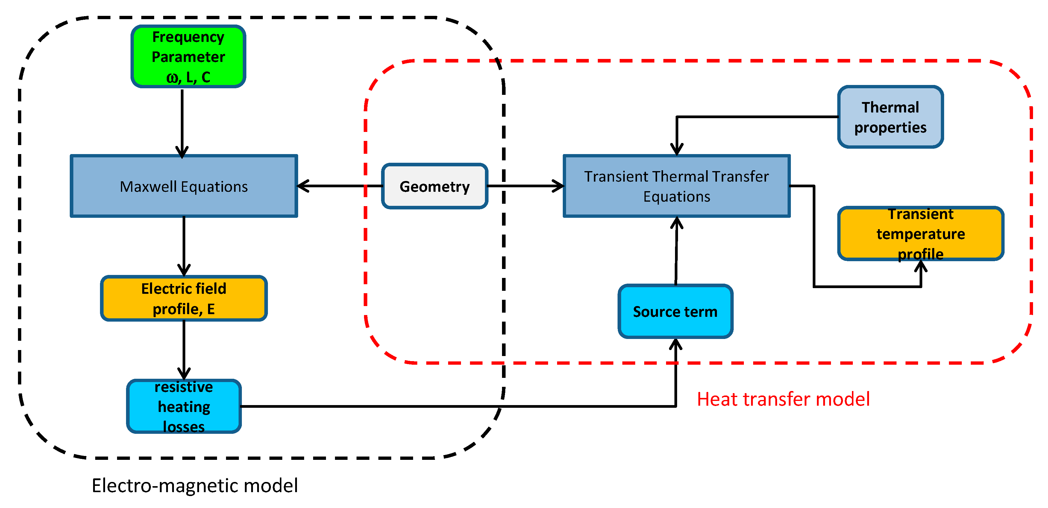
Strong coupling is ensured by applying the frequency-transient study. Ampere’s law is solved for each time step and then the thermal problem is solved for a transient state. As schematically shown in Figure 6, the eddy current simulation is linked to the thermal simulation to provide a complete solution for induction heating problems. Solving Maxwell’s equations for a given frequency and current density in the copper coils provides magnetic and electric field distributions within the geometry. Resistive heat losses obtained from Maxwell’s equation consist of the source term in the transient thermal transfer equations. The heating time was set to 60 s and the simulation parameters are summarized in Table 2.

3. Materials and Methods

According to the design discussed above, we build a specific reactor heated by electromagnetic induction for graphene synthesis. The input power was supplied by a 2.4 kW Easyheat (Ambrell) Generator that generates a high-frequency alternating electric current at a variable frequency of up to 250 kHz and with a maximum current of 450 A. The input gases composed by the CH4/H2/Ar mixture, depending on the process step, were fed with electronically controlled mass flow rate via MFC Brooks controllers and software. The Helmholtz coils include two identical circular magnetic coils each having two turns and fed by the generator. Each coil carries an equal electric current in the same direction. A flow of demineralized water at 40 °C is circulated by the heat exchanger in the compound circuit of the generator to limit the power losses of the inductive heating and to avoid the melting of the coil. The reactor chamber consists of two quartz tubes, one inside the other. The substrate used for the graphene synthesis was 125 μm thick oxygen-free high conductivity (OFHC) copper foil (99.95+% purity and a variable size from 1.35 × 1.35 cm2 to 1.35 × 1.70 cm2) inserted into the small mobile tube which serves as substrate support. The inner tube with 1.35 cm inner diameter has the advantages of faster and easier placing and removing of the substrate. It limits the contamination of the large fixed tube which seals the reactor and also makes easy the cleaning of the evaporated copper from the small diameter tube. The reactor was connected to a Pfeiffer brand pump operating at a maximum frequency of 1500 Hz. The role of the pumping system was to ensure a primary vacuum (10−3 mbar) and a secondary vacuum (up to 10−7 mbar) in the reactor enclosure as well as to maintain the pressure at the desired level. During all of the experiments, the substrate temperature was monitored by optical pyrometer (Yokogawa) with an optical resolution of 45:1, a thermal resolution of 0.1 °C, and a response time of 2 ms, placed above the substrate. Figure 7 shows the RF coil used in our induction heating system and a heated copper foil inside the quartz tube. As only the copper foil is heated, the temperature of the external quartz tube was less than 350 °C.
Before the experiment, the substrate was first ultrasonically cleaned in acetone for 15 min, then rinsed by acetone and isopropyl alcohol and finally blow-dried with nitrogen gas.

4. Results

4.1. Experimental Results

A typical synthesis process included three steps: (i) thermal annealing, followed by (ii) graphene deposition and (iii) cooling. During the annealing step, the copper foil can reach a temperature of ~ 1070 °C from room temperature within ~60 s. The pressure was maintained at 150 mbar under 500 sccm (standard cubic centimeters per minute) of argon mixed with 50 sccm of hydrogen. The annealing step lasts 500 s, which is sufficient to reduce oxygen and/or water contaminants on the substrate by using the hydrogen flow. After the annealing step, nucleation occurs and growth step with a typical duration of 150 s. During this step, the pressure was always maintained at 150 mbar under 100 sccm methane used as gaseous precursors mixed with 400 sccm of argon and 50 sccm of hydrogen. To stop the graphene growth process, we simultaneously cut off the source of carbon and the power source.
Synthesized graphene on copper was then transferred onto a SiO2/Si substrate with 300 nm thermal oxide, with poly(methyl methacrylate) (PMMA) as support. The PMMA/graphene/copper sample was first plunged in an acid solution for approximately four hours. The copper foil was completely dissolved in the acid, and the graphene foil combined with the mechanical reinforcement (PMMA) floats on the surface of the acid solution. After cleaning the PMMA/graphene in deionized water to remove any trace of copper etchant, it was transferred on SiO2/Si substrate and cleaned with acetone to remove the PMMA.
A typical Raman spectrum of a graphene film after the transfer is shown in Figure 8a. The main features in the graphene Raman spectra are peaks D (1333 cm−1), G (1580 cm−1), and 2D (2660 cm−1), in correspondence with Raman shifts. The D’ peak (1620 cm−1) originates from intra-valley one-phonon and is caused by the disordered structure of graphene. Therefore, both D and D’ peaks require a defect for their activation. Graphene edges also constitute a kind of defect due to the broken translational symmetry. Besides peaks D, D’, G, and 2D, other weak Raman modes can also be observed including an asymmetrical Raman D+D″ peak observed at (~2450 cm−1), whose intensity is comparable to that of the 2D’ peak at (~3400 cm−1) arising from the intravalley two longitudinal optical (LO) phonons [19]. Raman mapping in Figure 8b was performed in 50 × 50 μm2 and shows a relatively low defects ID/IG ratio. These defects refer to anything that breaks the symmetry of the infinite carbon honeycomb lattice such as graphene edges, grain boundaries, vacancies, implanted atoms, and defects associated with a change of carbon hybridization [20]. Raman mapping in Figure 8c,d shows high I2D/IG ratio, and a 2D bandwidth in the range of ~30 cm−1 to ~70 cm−1. Figure 9 shows statistics of mono-, bi-, and multilayer graphene films obtained from I2D /IG mapping. The calculated fraction of the surface with I2D/IG higher than 1 is ~42.3%, indicating the fraction of monolayer graphene in these samples. Many areas were found to have bilayers (40.6%) and multilayers (17.1%). These values are comparable to those of the thermal CVD-grown few-layer (2–3) graphene films [21] and better than of the PECVD [22]. Bi- and multilayer graphene could be formed by secondary nucleation on monolayer graphene domains. Nevertheless, bilayer graphene may play an important role in electronic devices where its additional “layer” degree of freedom could be manipulated to achieve desirable properties [23].
To elucidate the nucleation step, SEM analysis was performed on graphene grown on polycrystalline copper after only 5 s of methane addition. The nucleation of graphene occurs after the supersaturation of active carbons, and then domain growth is started.
From Figure 10, we can easily identify the graphene domains and the growth front. Even only after 5 s deposition, a big part of the substrate surface is covered with graphene sheets attesting of high nucleation rate. With the growth time, these isolated sheets percolate and form single layer graphene. The boundaries between two grains are made of defects such as pentagons and heptagons where the carbon–carbon bonds are strained. According to Vlassiouk et al. [24], hydrogen concentration controls the size and morphology of the resulting graphene domains in the thermal CVD process. Nevertheless, the separation of the nucleation and growth steps remains difficult to control regardless of the activation process.
As shown in the SEM pictures of Figure 10, at the first nucleation stages, small graphene domains are formed and tend to collapse at the end of the growth. The optimization of the growth time is very important in order to cover the entire substrate surface avoiding secondary nucleation. The Raman mapping of Figure 8c was performed on a sufficiently large surface area 50 × 50 μm2 to statistically cover edges as well as centers of graphene domains. The I2D/IG ratio of 2.14 obtained from Figure 8a is reproducible at the macroscopic scale of the sample and in both upper and bottom copper sides. In addition to Raman, other characterization techniques were proposed in the literature to determine the quality of graphene/SiO2 substrates. Castriota et al. used the Angle Spectroscopic Ellipsometry (VASE) technique to study the optical properties of monolayer CVD graphene transferred from native copper substrate onto SiO2 (287 nm thick)/Si substrates [25]. The graphene was modeled as the sum of Lorentz oscillators with parameters estimated experimentally at different angles of incidence in the broad energy range from 0.38 eV to 6.2 eV. The proposed model corroborates well their micro-Raman measurements. Furthermore, authors mentioned that structural imperfections as grain boundaries, defects, residues from transfer, and bilayer and multilayer graphene patches could cause some variations in the optical constants. The estimated carrier density obtained from optical conductivity data is ~ 7.8 × 1013 cm−2, indicating unintentional doping those authors eventually attributed to residual metallic contamination, the SiO2 substrate effect, and impurities such as H2O or PMMA residues. To overcome transfer contamination, Liu et al. reported graphene growth by chemical vapor deposition on SiO2 without any metal catalysts. Raman spectroscopy and mapping confirm the weak defect and good quality with monolayer, bilayer, and few-layer graphene with a high coverage over ~95% [26]. Nevertheless, graphene growth by this technique strongly depends on the H2 flow rate and the growth time of up to 16 h is much higher than in inductive heating. Regardless of the growth process, as monolayer graphene is polycrystalline, defects are naturally present in the boundaries that connect different grains with different orientations. These boundaries are mainly formed by strained pentagons and heptagons of carbon atoms tending to form continuous graphene from non-defective subdomains of average size La. The size of these domains is detrimental to electron transport. As most of the potential applications of graphene are dependent on large non-defective subdomains, a theoretical model supported by experimental results was proposed in [27] to correlate the graphene crystallite sizes La with the Raman ID/IG ratio between the defect-induced (D band) modes and the C–C stretching (G band) via the following equation,
La ( nm ) = 560 E λ   . I D I G ,
where Eλ is the excitation laser energy used in the Raman experiment in eV units.
When applied to our samples, Equation (20) produces values of La=158 ± 9 nm comparable with the literature. In particular, Vlassiouk et al. [28] studied the effect of disorder in low temperature thermal CVD graphene by varying either growth temperature (750–1000 °C), the catalyst nature (Ni, Cu), and the carbon source (CH4, C2H2). Their less defective graphene was obtained at 1000 °C with Cu as catalyst and CH4 as carbon source with 0.077 < ID/IG < 0.334 ratios obtained from Raman spectra recorded at 633 nm. The ID/IG ~0.24 obtained from our results at the same Raman wavelength is in the same range. For CVD graphene transferred onto SiO2 substrates, the bulk graphene resistivity ρ, was measured by the four-point probe technique and correlated to crystallite size La by Vlassiouk et al. [28] through the equation
ρ ( Ω ) = 6.7 10 5 La   ( nm ) ,
Using fit through Equation (21), we obtained an electrical resistivity of ρ~4.2 × 10³ Ω lower than theoretical resistivity of pristine graphene, πh/4e2 ~20 kΩ. This leads to electrical conductivity of σ~2.4 × 10⁻⁴ Ω−1 in the standard range of CVD graphene electrical conductivities 3 × 10⁻⁶ Ω−1 < σ < 10−3 Ω−1 [28]. Another method of estimating the conductivity of arbitrarily stacked graphene sheets was proposed from semi-classical Boltzmann transport theory [23,29,30]. This model correlates the resistivity to surface defect concentration, nd (cm−1) by the equation
ρ = ( 2   e 2 π h   n n d   ln 2   ( k F R )   ) 1 ,
where R is the radius of the defects’ potential well in the same magnitude than the dimensions of carbon cycles ~0.4 nm, k F = n   π is the Fermi wave vector, n is the electron concentration, e is the electron charge, and h is Planck’s constant. Electron concentration n could be as high as 1013 cm−2 in exfoliated graphene and 1012 cm−2 for CVD graphene [28], whereas defect density nd varies from ~1010 cm−2 in suspended graphene to ~1014 cm−2 for very defective graphene [23]. By combining Equation (21) and Equation (22), the concentration of defects could be correlated to the crystallite size La by nd ~½ R La [28].

4.2. Modeling Results

The resolution of the model equations with boundary conditions has been performed using 2D finite element method for the parameter of Table 2 using COMSOL software. The temperature distribution after 60 s (at the end of the heating period) is shown in Figure 11a. We can see that the heating is concentrated around the copper foil. The time evolution of the average temperature of the copper foil during the heating period is shown in Figure 11b. The maximum temperature of 1040 °C is reached after about 30 s. For similar operating conditions, the calculated temperatures are very close to the experimentally measured ones (1040 °C).
The surface plot of the magnetic flux density norm; the magnetic flux lines distribution are shown in Figure 12.
The magnetic flux density near the coil is significantly greater than the magnetic flux density around the copper foil. Figure 13 shows the current density contours along the copper foil. Non uniform current distribution within the copper foil cross section is considered through “skin effect”. The maximum value of the current density is located on the copper surface and the current density decreases from the body surface toward its center. It can be seen that the current density is higher in the copper foil periphery region.
Experimental substrate temperature evolution versus time was compared to simulation (Figure 14) and shows a good agreement. Experimental heating rate (~25 °C/s) and cooling rate (as high as ~73 °C/s) avoid the formation of multilayered graphene during the cooling step. Therefore, the major advantages of the electromagnetic induction CVD system are localized heating and fast cooling rate.
Finally, to study the simultaneous effect of the size of the copper foil and the current, simulations were performed in a pure Ar and Ar/H2 mixture. Figure 15 shows the contour maps of isotherms obtained by varying the radius r(m) of the copper foil and the current, I(A).
The domain delimited by isotherms 1035 °C and 1084 °C is supposed to provide good graphene quality. At a temperature higher than 1084 °C, the copper foil melts, whereas at a temperature lower than 1035 °C, graphene with several defects and poor structural quality is obtained. We can notice that for a given current, adding hydrogen to the argon shift the graphene domain to the higher substrate sizes, in agreement with experimental observations.
Therefore, the use of computer models for the performance predictions provides an excellent tool for the design and the management of graphene growth by inductively heated copper substrate. Other materials, such as Ni, Co, Mo, Au, and W, are under study to test their thermal capacities before studying their catalytic activities to decompose methane via inductively heated set up.
In addition, large-scale graphene production by inductive heating is feasible and has the potential to be economically viable. According to the Equations (9) and (10), given a current I and a frequency f, as the copper foil radius r, the radius of the turns R and the spacing between turns H are simultaneously increased by a factor k, the power transferred to the copper foil QA, and the power provided to the coils QB will be scaled-up by factors k2 and k, respectively. For example, a 100 kW generator would heat a copper foil of radius up to ~1 m. Even in industry, large scale heating of metals is routinely done via magnetic inductive heating systems with power ranging from 250 kW to 20,000 kW. To enable mass production of graphene-based devices, the batch process could be replaced by a continuous roll-to-roll (R2R) manufacturing. Taking advantage of the fast heating of inductive systems, energetic efficiency as well as thermal homogeneity can be improved via the optimization of the speed of the moving copper foil in the hot coil zone during (R2R) processing [31].

5. Discussion

We focused the present study on the combined effects of substrate size and applied current in order to determine the optimal window to grow graphene. Nevertheless, other factors affect the quality of graphene such as gas feeding ratio, pressure, or substrate chemical nature. A possible way to increase the percentage of monolayer graphene is to lower the nucleation density. In this direction, passivation of the copper surface by increasing the thickness of the Cu2O layer through heating the copper foil at ambient atmosphere allowed to drastically decrease the nucleation density, thereby increasing single crystal size up to few millimeters [32]. Regarding our preliminary question: to grow graphene from methane should we decompose the gaseous precursor by heating the gas in the volume or can the catalyst directly make this decomposition without the need to heat the overall surrounding gas? We compared temperature profiles issued from our PECVD process with a 2.45 GHz microwave [33,34] with actual calculations in inductive heating process. To depict the influence of the thermal design on the methane decomposition performances of axisymmetric PECVD and inductively heated reactors, we first compared temperature profiles above the substrate in these processes. Despite the different geometries and catalysts involved, calculated temperature profiles above the substrate of Figure 16 shows a radically opposite behavior. In PECVD reactor Figure 16a, the temperature is maximum at ~1.7 cm with a positive temperature gradient from the substrate. In inductively heated reactor, the temperature gradient is negative and temperature rapidly decreases from 1050 °C at the substrate to ~600 °C at a distance 0.7 cm from the substrate as reported in Figure 16c. Therefore, the direction of the temperature gradient across the substrate is upward and downward in PECVD (Figure 16b) and inductively heated reactors (Figure 16d), respectively. This induces differences in methane decomposition kinetics thereby affecting graphene growth modes. In inductively heated reactor, we calculated using ANSYS Chemkin-Pro Software [35] the distribution of species above the substrate in the specific graphene growth conditions. These preliminary calculations are based on gas phase chemistry without yet surface reactions. As clearly shown in Figure 16e, the majority of the injected methane (73% molar) reaches the catalyst and constitutes the major carbon species feedstock with ~0.14 CH4 mole fraction. In comparison, in PECVD all the injected methane is transformed to acetylene which constitutes the major carbon species at the substrate ~0.01 C2H2 mole fraction [33]. Therefore, the activation of the system by thermal, plasma, or induction has a direct impact on nucleation and growth kinetics. In the case of inductive heating, it is therefore not necessary to decompose the methane and there is no need to heat the overall surrounding gas to obtain good quality graphene as demonstrated by our experimental results.
Furthermore, a quantitative understanding of graphene growth necessitates considering gas-phase and surface chemistries. We are actually developing a (3D) modeling approach, including detailed chemistries, in order to explain the temperature-dependent growth kinetics of graphene formation on copper substrates inductively heated. Simulations are performed to determine the gas phase fields for temperature and species concentration as well as the surface-species coverage and graphene growth rate.

6. Conclusions

This work is a contribution to the reactor design for graphene synthesis by electromagnetic induction where RF field directly heats the catalytic copper foil. We used numerical simulations of electromagnetic and thermal magnitudes, as well as the interpretation of the physical phenomena involved during a specific induction heating process for graphene synthesis. Indeed, despite its many advantages, the control of this type of heating requires a perfect knowledge of the spatial distribution and the temporal evolution of the electromagnetic field and temperature during the growth. We have also demonstrated the growth of high-quality graphene films using inductive heating. The copper foil can reach 1050 °C from room temperature within 1 min. This process is faster, cheaper, and more energy-saving than the most commonly used hot-wall CVD method. While injecting the methane at ~1050 °C, a thin film of carbon is thought to nucleate and grow at the copper surface. At the end of the experiment, high cooling rates of 70 °C/s allow the growth process to be instantaneously stopped by cutting off the power source and the gas flow rates avoiding secondary graphene nucleation. Raman spectroscopy was used to determine the graphene quality with around 42.3% monolayer graphene. Separate experiments were performed to study the early nucleation step by Scanning electron microscope (SEM). Well-defined graphene domains were observed after only 5 s, suggesting high nucleation rates. Based on these results, the subsequent experiments should be performed with reduced deposition time. This could be combined with more detailed studies on other graphene growth influential parameters. The accurate 2D transient model was also solved for coupled induction heating reactor designed to study the electromagnetic field distribution, eddy currents density and heating pattern in a 125 μm thick copper foil. From the obtained results we can conclude that the model accurately predicts the spatial structure of the electromagnetic field as well as temperature distribution in the RF-coil geometry. The model was validated using experimental data. This model can be used as a predictive tool for future developments.
One important result from this study is obtained by comparing inductive heating with conventional thermal or plasma CVD. To obtain graphene, the later processes need high temperatures to dissociate methane due to the high barrier energy for breaking the C–C and C–H bonds. In inductive heating, it is not necessary to heat the gas surrounding the copper at elevated temperatures. The copper is able to dissociate methane at a temperature of 1050 °C. Due to its simplicity and efficiency, the inductive heating is perfectly suited to the scale-up for industrial graphene manufacturing. In addition, the reactor concept could be easily adapted to any gaseous, liquid or solid precursors. In particular, the possibility to synthesis other 2D materials such as BN or WS2, with the same concept is currently under study.

Author Contributions

Conceptualization, S.F. and Y.R.; software, I.H.; investigation, K.P. and E.D.; data curation, K.P. and E.D.; writing—original draft preparation, K.P.; writing—review and editing, All authors; visualization, O.B. and K.P.; supervision, I.H., M.A., and S.F. All authors have read and agreed to the published version of the manuscript.

Funding

This research was funded by ANR (Agence Nationale de la Recherche) grant numbers ANR 11 IDEX 05 02, and ANR-14CE08-0018.

Acknowledgments

ANR (Agence Nationale de la Recherche) and CGI (Commissariat à l’Investissement d’Avenir) are gratefully acknowledged for their financial support of this work through Labex SEAM (Science and Engineering for Advanced Materials and devices) ANR 11 LABX 086, ANR 11 IDEX 05 02, and ANR-14CE08-0018. L’Agence Universitaire de la Francophonie (AUF) and the Fund “Scientific Research”, Bulgaria are gratefully acknowledged for their financial support of this work (bilateral project TherMoVapCar). European Union (EU) is gratefully acknowledged for funding through international mobility program Erasplus+.

Conflicts of Interest

The authors declare no conflict of interest.

References

  1. Amjadi, M.; Kyung, K.U.; Park, I.; Sitti, M. Stretchable, skin-mountable, and wearable strain sensors and their potential applications: A review. Adv. Funct. Mater. 2016, 26, 1678–1698. [Google Scholar] [CrossRef]
  2. Ho, D.H.; Sun, Q.; Kim, S.Y.; Han, J.T.; Kim, D.H.; Cho, J.H. Stretchable and multimodal all graphene electronic skin. Adv. Mater. 2016, 28, 2601–2608. [Google Scholar] [CrossRef] [PubMed]
  3. Hou, C.; Wang, H.; Zhang, Q.; Li, Y.; Zhu, M. Highly conductive, flexible, and compressible all-graphene passive electronic skin for sensing human touch. Adv. Mater. 2014, 26, 5018–5024. [Google Scholar] [CrossRef]
  4. Tung, T.T.; Castro, M.; Kim, T.Y.; Suh, K.S.; Feller, J.F. Graphene quantum resistive sensing skin for the detection of alteration biomarkers. J. Mater. Chem. 2012, 22, 21754–21766. [Google Scholar] [CrossRef]
  5. Wu, C.; Feng, J.; Peng, L.; Ni, Y.; Liang, H.; He, L.; Xie, Y. Large-area graphene realizing ultrasensitive photothermal actuator with high transparency: New prototype robotic motions under infrared-light stimuli. J. Mater. Chem. 2011, 21, 18584–18591. [Google Scholar] [CrossRef]
  6. Vlassiouk, I.; Smirnov, S.; Surwade, S.P.; Regmi, M.; Srivastava, N.; Feenstra, R.; Eres, G.; Parish, C.; Lavrik, N.; Datskos, P.; et al. Graphene nucleation density on copper: Fundamental role of background pressure. J. Phys. Chem. C 2013, 117, 18919. [Google Scholar] [CrossRef]
  7. Novoselov, K.S.; Geim, A.K.; Morozov, S.V.; Jiang, D.; Zhang, Y.; Dubonos, S.V.; Grigorieva, I.V.; Firsov, A.A. Electric field effect in atomically thin carbon films. Science 2004, 306, 666–669. [Google Scholar] [CrossRef] [Green Version]
  8. Piner, R.; Li, H.; Kong, X.; Tao, L.; Kholmanov, I.N.; Ji, H.; Lee, W.H.; Suk, J.W.; Ye, J.; Hao, Y.; et al. Graphene synthesis via magnetic inductive heating of copper substrates. ACS Nano 2013, 7, 7495–7499. [Google Scholar] [CrossRef]
  9. Seifert, M.; Drieschner, S.; Blaschke, B.M.; Hess, L.H.; Garrido, J.A. Induction heating-assisted repeated growth and electrochemical transfer of graphene on millimeter-thick metal substrates. Diam. Relat. Mater. 2014, 47, 46–52. [Google Scholar] [CrossRef]
  10. Wu, C.; Li, F.; Chen, W.; Veeramalai, C.P.; Ooi, P.C.; Guo, T. Electromagnetic induction heating for single crystal graphene growth: Morphology control by rapid heating and quenching. Sci. Rep. 2015, 5, 9034. [Google Scholar] [CrossRef]
  11. Sosnowchik, B.D.; Lin, L. Rapid synthesis of carbon nanotubes via inductive heating. Appl. Phys. Lett. 2006, 89, 193112. [Google Scholar] [CrossRef]
  12. Rudnev, V.; Loveless, D.; Cook, R.; Black, M. Handbook of Induction Heating; Marcell Dekker Inc.: New York, NY, USA, 2003; pp. 99–183. [Google Scholar]
  13. Tari, A. The Specific Heat of Matter at Low Temperatures; Imperial College Press: London, UK, 2003; p. 37. [Google Scholar]
  14. CRC Handbook of Chemistry and Physics, 65th ed.; Weast, R.C.; Astle, M.G.; Beyer, W.H. (Eds.) CRC Press, Inc.: Boca Raton, FL, USA, 1984; pp. F-114–F-120. [Google Scholar]
  15. Schlichting, H. Boundary Layer Theory, 7th ed.; McGraw Hill Book Company: New York, NY, USA, 1979. [Google Scholar]
  16. Holman, J.P. Heat Transfer, 7th ed.; McGraw Hill Book Company: New York, NY, USA, 1990. [Google Scholar]
  17. Zhao, L.; Zhang, R.; Deng, C.; Peng, Y.; Jiang, T. Tunable infrared emissivity in multilayer graphene by ionic liquid intercalation. Nanomaterials 2019, 9, 1096. [Google Scholar] [CrossRef] [Green Version]
  18. Baranova, P.; Baranova, V. Modeling axial 8-coil system for generating uniform magnetic field in COMSOL. In MATEC Web of Conferences; EDP Sciences: Les Ulis, France, 2016; Volume 48, p. 03001. [Google Scholar]
  19. Wu, J.B.; Lin, M.L.; Cong, X.; Liu, H.N.; Tan, P.H. Raman spectroscopy of graphene-based materials and its applications in related devices. Chem. Soc. Rev. 2018, 47, 1822–1873. [Google Scholar] [CrossRef] [PubMed] [Green Version]
  20. Eckmann, A.; Felten, A.; Mishchenko, A.; Britnell, L.; Krupke, R.; Novoselov, K.S.; Casiraghi, C. Probing the nature of defects in graphene by Raman spectroscopy. Nano Lett. 2012, 12, 3925–3930. [Google Scholar] [CrossRef] [PubMed] [Green Version]
  21. Ferrari, A.C.; Meyer, J.C.; Scardaci, V.; Casiraghi, C.; Lazzeri, M.; Mauri, F.; Piscanec, S.; Jiang, D.; Novoselov, K.S.; Roth, S.; et al. Raman spectrum of graphene and graphene layers. Phys. Rev. Lett. 2006, 97, 187401. [Google Scholar] [CrossRef] [Green Version]
  22. Mehedi, A.; Baudrillart, B.; Alloyeau, D.; Mouhoub, O.; Ricolleau, C.; Pham, V.D.; Chacon, C.; Gicquel, A.; Lagoute, J.; Farhat, S. Synthesis of graphene by cobalt-catalyzed decomposition of methane in plasma enhanced CVD: Optimization of experimental parameters with Taguchi method. J. Appl. Phys. 2016, 120, 065304. [Google Scholar] [CrossRef]
  23. Min, H.; Jain, P.; Adam, S.; Stiles, M.D. Semiclassical Boltzmann transport theory for graphene multilayers. Phys. Rev. B 2011, 83, 195117. [Google Scholar] [CrossRef] [Green Version]
  24. Vlassiouk, I.; Regmi, M.; Fulvio, P.; Dai, S.; Datskos, P.; Eres, G.; Smirnov, S. Role of hydrogen in chemical vapor deposition growth of large single crystal graphene. ACS Nano 2011, 5, 6069–6076. [Google Scholar] [CrossRef]
  25. Castriota, M.; Politano, G.G.; Vena, C.; De Santo, M.P.; Desiderio, G.; Davoli, M.; Cazzanelli, E.; Versace, C. Variable angle spectroscopic ellipsometry investigation of CVD-grown monolayer graphene. Appl. Surf. Sci. 2019, 467–468, 213–220. [Google Scholar] [CrossRef]
  26. Liu, Q.; Gong, Y.; Wang, T.; Chan, W.L.; Wu, J. Metal-catalyst-free and controllable growth of high-quality monolayer and AB-stacked bilayer graphene on silicon dioxide. Carbon 2016, 96, 203–211. [Google Scholar] [CrossRef] [Green Version]
  27. Cancado, L.G.; Takai, K.; Enoki, T.; Endo, M.; Kim, Y.A.; Mizusaki, H.; Jorio, A.; Coelho, L.N.; Magalhaes-Paniago, R.; Primenta, M.A. General equation for the determination of the crystallite size of nanographite by Raman spectroscopy. Appl. Phys. Lett. 2006, 88, 163106. [Google Scholar] [CrossRef]
  28. Vlassiouk, I.; Smirnov, S.; Ivanov, I.; Fulvio, P.F.; Dai, S.; Meyer, H.; Chi, M.; Hensley, D.; Datskos, P.; Lavrik, N.V. Electrical and thermal conductivity of low temperature CVD graphene: The effect of disorder. Nanotechnology 2011, 22, 275716. [Google Scholar] [CrossRef] [PubMed]
  29. Chen, J.H.; Cullen, W.G.; Jang, C.; Fuhrer, M.S.; Williams, E.D. Defect scattering in graphene. Phys. Rev. Lett. 2009, 102, 236805. [Google Scholar] [CrossRef] [PubMed]
  30. Stauber, T.; Peres, N.M.R.; Guinea, F. Electronic transport in graphene: A semiclassical approach including midgap states. Phys. Rev. B 2007, 76, 205423. [Google Scholar] [CrossRef] [Green Version]
  31. Alrefae, M.A.; Kumar, A.; Pandita, P.; Candadai, A.; Bilionis, I.; Fisher, T.S. Process optimization of graphene growth in a roll-to-roll plasma CVD system. AIP Adv. 2017, 7, 115102. [Google Scholar] [CrossRef] [Green Version]
  32. Zhou, H.; Yu, W.J.; Liu, L.; Cheng, R.; Chen, Y.; Huang, X.; Liu, Y.; Wang, Y.; Huang, Y.; Duan, X. Chemical vapour deposition growth of large single crystals of mono-layer and bilayer graphene. Nat. Commun. 2013, 4, 2096. [Google Scholar] [CrossRef] [Green Version]
  33. Hinkov, I.; Pashova, K.; Farhat, S. Modeling of plasma-enhanced chemical vapor deposition growth of graphene on cobalt substrates. Diam. Relat. Mater. 2019, 93, 84–95. [Google Scholar] [CrossRef]
  34. Pashova, K.; Hinkov, I.; Aubert, X.; Prasanna, S.; Bénédic, F.; Farhat, S. Graphene synthesis by microwave plasma chemical vapor deposition: Analysis of the emission spectra and modeling. Plasma Sources Sci. Technol. 2019, 28, 045001. [Google Scholar] [CrossRef]
  35. Kee, R.J.; Rupley, F.M.; Miller, J.A.; Coltrin, M.E.; Grcar, J.F.; Meeks, E.; Moffat, H.K.; Lutz, A.E.; Dixon-Lewis, G.; Smooke, M.D.; et al. CHEMKIN Collection, Release 3.6; Reaction Design, Inc.: San Diego, CA, USA, 2001. [Google Scholar]
Figure 1. Inductive heating set-up: (a) Top and side views of the circular magnetic induction coils placed symmetrically on both sides of a thin copper foil; (b) Schematic drawing of Helmholtz coils used for the inductive heating; (c) Simplified configuration used for the uniformity calculation of the magnetic field where the coils with closed geometry with a circular cross section perpendicular to the z-axis are placed symmetrically with respect to the median plane of the substrate at positions Q1, Q2, Q3, and Q4 along the z-axis and connected in series with the current source; (d) Cross section of the coils showing the perpendicular magnetic field and orthonormal electric field.
Coatings 10 00305 g001
Figure 2. Actual copper thickness as compared to calculated skin depths, at different operating frequencies.
Coatings 10 00305 g002
Figure 3. Effect of the gas composition and inlet flowrate on the convective heat transfer around a copper foil.
Coatings 10 00305 g003
Figure 4. (a) Axial distribution of the magnetic field Bz. (b) Relative uniformity δz along z axis. (c) Radial distributions of the magnetic field Bz. (d) Relative uniformity δx along x axis. Calculated in the geometry of Figure 1c with 4 loops centered at zQ = −31.5, −18.1, 18.1, 31.5 mm, the loop radius is R = 18.1 mm, the current in each loop is I = 77.4 A.
Coatings 10 00305 g004
Figure 5. (a) Photography of the reactor; (b) Object geometry of the induction heating system; (c) Finite element mesh of the computational domains with the copper foil in the middle of the coils where water flows (cross section configuration). Fine grid is placed in the areas where strong gradients are expected.
Coatings 10 00305 g005
Figure 6. Flowchart of solving strategy of the coupled electromagnetic Maxwell’s equations and thermal equation in transient. The heat is generated by eddy currents, which flow through copper foil and create a Joule heat I2R.
Coatings 10 00305 g006
Figure 7. Induction reactor set-up: (a) Photograph of RF graphene growth set-up including a gas injection system, RF heating coils, power supply, chiller, reaction chamber, optical pyrometer, and a vacuum pumping system; (b) Photography of RF coils and a heated copper foil supported by the inner quartz tube. The gas flows in the inner and the outer quartz tubes.
Coatings 10 00305 g007
Figure 8. Raman spectroscopy in confocal mode in air with the backscattering configuration using 632.8 nm laser excitation at room temperature. Copper foil size 1.35 × 1.70 cm2, current intensity for annealing I = 268 A and for growth I = 288 A, and frequency f = 215 kHz. Temperature was fixed at 1040 °C, and annealing and growth time were 500 s and 150 s, respectively: (a) Typical Raman spectra of transferred graphene onto SiO2/Si substrate; (b) Raman mapping of ID/IG ratio; (c) Raman mapping of I2D/IG ratio; (d) Raman mapping of 2D bandwidth (FMWH) unit is cm−1.
Coatings 10 00305 g008
Figure 9. Statistics of mono-, bi-, and multilayer graphene films obtained from I2D/IG in Raman mapping. In insert, Raman mapping images of graphene film on a SiO2/Si substrate.
Coatings 10 00305 g009
Figure 10. SEM images at different magnifications of graphene grown on copper foil after 5 s deposition time: (a) 5000 X; (b) 6780 X; (c) 10,000 X and (d) 25,000 X.
Coatings 10 00305 g010
Figure 11. (a) Temperature distribution in the induction heating system after 60 s. (b) Calculated copper foil surface temperature evolution during heating.
Coatings 10 00305 g011
Figure 12. (a) Magnetic flux density during the transient study. (b) Magnetic flux lines distribution.
Coatings 10 00305 g012
Figure 13. Current density contours along the copper foil.
Coatings 10 00305 g013
Figure 14. Comparison between the experimental data and the prediction coming from the simulation.
Coatings 10 00305 g014
Figure 15. Simultaneous effect of copper foil size and electrical current intensity on substrate temperature: (a) Pure argon; (b) Mixture of 500 sccm argon with 100 sccm H2.
Coatings 10 00305 g015
Figure 16. (a) Calculated temperature distribution above cobalt substrate in several PECVD conditions: 50 sccm H2; 1 or 10 sccm CH4; chamber pressure was maintained at 8 mbar for 300 W and 13 mbar for 400 W in order to maintain a constant plasma volume. Substrate temperature was 700 °C and 850 °C [33]; (b) PECVD thermal boundary layer shape; (c) Calculated temperature distribution above copper substrate heated at 1050 °C by inductive heating process. (d) Inductive heating thermal boundary layer shape. (e) Calculated mole fraction distribution using ANSYS Chemkin-Pro Software at pressure P = 150 mbar and inlet flowrates of 400 sccm Ar, 50 sccm H2, and 100 sccm CH4. Substrate temperature was fixed at 1050 °C.
Coatings 10 00305 g016
Table 1. Calculated convective heat transfer around a copper foil at different reactor conditions 1.
Condition 1Flowratesv, m.s−1RePrNuh, W·m−2·K−1
1500 sccm Ar0.3375.790.671.364.1
2500 sccm H20.3370.800.680.5216.6
3500 sccm CH40.3374.620.451.0910.9
450 sccm H2 0.0340.080.680.175.2
5100 sccm CH40.0670.920.450.494.9
6500 sccm Ar + 50 sccm H2 0.376.730.391.267.1
7400 sccm Ar + 50 sccm H2 + 100 sccm CH40.377.030.371.268.7
1 with v the flow velocity estimated from the flowrate and h the convective heat transfer coefficient estimated from Equations (11) and (12). Re, Pr, and Nu are Reynolds, Prandtl, and Nusselt dimensionless numbers, respectively.
Table 2. Simulation parameters.
ParameterSymbolValue
Coil current (A)Ic269
Frequency (kHz)f250
Heating time (s)t60
Copper foil radius (cm)rf0.675
Copper foil height (μm)hf125
Coil inner radius (mm)rin2.1
Coil wall thickness (mm)sc1
Distance between coils (mm)dc30.4
Distance between coil turns (mm)dt7.2
Number of coil turnsN2

