Article

Analysis of Machinability and Crack Occurrence of Steels 1.2363 and 1.2343ESR Machined by Die-Sinking EDM

1
Faculty of Mechanical Engineering, Brno University of Technology, 616 69 Brno, Czech Republic
2
Faculty of Production Technologies and Management, Jan Evangelista Purkyně University, 400 96 Ústínad Labem, Czech Republic
3
Department of Production machines and design, Technical University of Ostrava, 708 33 Ostrava, Czech Republic
*
Author to whom correspondence should be addressed.
Coatings 2020, 10(4), 406; https://doi.org/10.3390/coatings10040406
Submission received: 28 March 2020 / Revised: 15 April 2020 / Accepted: 17 April 2020 / Published: 19 April 2020

Abstract

:
Die-sinking electric discharge machining (EDM) is an indispensable technological operation, especially in the production of molds and all internal and external shapes and cavities. For this reason, the effect of machine parameter settings (open-voltage, pulse current, pulse on time, and pulse off time) on the machining of two types of steels, 1.2363 and 1.2343ESR, was carefully investigated using graphite or copper electrodes in 10 mm × 10 mm or 100 mm × 100 mm shapes. For this purpose, a two-level half factor experiment was performed with one replication at the corner points and two replications at the central points, with a total of 80 rounds. The subject of the evaluation was the topography and morphology of machined surfaces including a detailed analysis of surface and subsurface defects in the form of cracks including the creation of regression equations describing the probability of crack occurrence. Furthermore, a study of the local hardness change in the subsurface area was performed, and lamellas were also made and studied by transmission electron microscopy. It has been found that by using die-sinking EDM, it is possible to effectively predict the probability of cracking on machined surfaces and also on machine 1.2363 and 1.2343ESR steels with a very good surface quality of Ra 1.9 and 2.1 µm using graphite electrodes. These findings will ensure the production of parts with the required surface quality without cracks, which is a crucial aspect for maintaining the required functionality and service life of the parts.

1. Introduction

Die-sinking electric discharge machining (EDM) is an unconventional machining technology that removes material using periodically repeating electrical pulses generated by the machine generator. Since the plasma channel is formed here, the workpiece material is exposed to very high temperatures in the range of 12,000–20,000 °C for a short time (within microseconds), which McGeough [1] presented in his study in 1988. The machining tool is an electrode, which has a negative workpiece shape and is most often made of copper or graphite. During the machining, the electrode and workpiece are immersed in a dielectric liquid, most often kerosene [2,3]. Any, at least electrically conductive, materials can be machined without any requirement for their hardness or toughness. Since there is a so-called eroding gap between the workpiece and tool, the tool does not affect the material to be machined by any mechanical force, as is the case with conventional machining. Therefore, it is possible to produce thin-walled profiles or to process very soft materials [4,5].
Nikalje [6] studied the impact of the parameters and EDM optimization based on Maraging steel 300 used as a material. The method of Taguchi was used to define the necessary outputs. It was found that the pulse on and off time, together with the discharge current, had a major effect on the EDM performance and operations. With the help of the scanning electron microscope (SEM) analysis, it was observed that the higher discharge current and pulse on time means a rougher surface is achieved, and vice versa. Rajendran [7] focused on the crack formation and resolidified layer, having used T90Mn2W50Cr45 tool steel as a base material that underwent EDM processing. Different process parameters were combined during the experiment. It was detected that the properties of the base material itself, together with the resolidified layer and electrode wear, affected the crack formation to a great extent. Majumderin [8] tried to optimize the parameters of the EDM process in their study by employing the particle swarm optimization approach based on fuzzy logic. They used AISI 316LN stainless steel as a base material. It was proven by the experiments that the strategy employed was appropriate and agreed well with the foreseen outputs. Gill [9] studied the quality of the surface on H11 die steel used as the experimental material, namely employing surface alloying as a successful method for EDM process analysis. The outputs of the experiments that were carried out utilizing different techniques like SEM, energy-dispersive X-ray spectroscopy (EDS), and X-ray diffraction (XRD) revealed that there were no cracks on the surface, and the microhardness was improved. Straka [10] used the statistical approach to investigate the optimization of the EDM process parameters. The study was performed based on the chrome–molybdenum–vanadium alloyed steel, the quality of which was evaluated taking into account the microhardness and surface roughness. Based on the outputs of the experiments, the mathematical models were defined using statistical methods. Santos [11] analyzed the surface integrity of nitriding the material of AISI 4140 steel, namely ion implantation, which proved to be very appropriate in the sink EDM process. They employed various techniques during the experiments, with SEM, XRD, and optical microscopy among them. Sidhom [12] focused their experiments on the final quality of the machined surface and the corrosion resistance by using authentic stainless steel as a base material for their experiments. The machining process of EDM led to substantial changes in the material such as microstructural, mechanical, chemical, and micro-geometrical. These changes affected the appearance of the white layer and heat-affected layer. Dewangan [13] carried out experiments to study the multi-response optimization of the integrity of the surface during the EDM process and employed the hybrid method for the investigation, using fuzzy logic and grey analysis. As a result, the optimal parameter settings were found, with the pulse on time being the most effective parameter. Dewangan [14] focused on the impact of various tool electrode materials on the processed surface integrity of AISI P20 tool steel, which was chosen as the experimental material. They employed various tool electrode materials, like graphite, brass, and copper. According to the outcomes of the experiments, the graphite tool induced the maximum of the surface crack density, white layer thickness, and surface roughness. D’Urso [15] dealt with the execution of micro-pockets on two different materials (AISI 316 L stainless steel and ZrC + 10MoSi2 UHT ceramic) using micro-EDM milling. Valentinčič [16] created a system for on-line selection of the machining parameters according to the given machining surface. Debnath [17] studied the wire electrical discharge machining (WEDM) process of machining 430 stainless steel and tap water was used as the dielectric medium to substitute hydrocarbon oil in the experiments. It was observed during the investigation that the increase in current and pulse on time led to the increase in the surface roughness and material removal rate, but the tool wear rate increased with the increase in current, and decreased when the pulse on time increased. Jarosz [18] studied the influence of process parameters on the surface roughness during the WEDM machining of hot-working Orvar supreme die steel. They employed various values of pulse current in the experiments to observe the surface roughness of the material. It turned out that there was a substantial link between the process parameter under investigation and the surface roughness. Valarmanthi [19] also focused on the surface roughness in their experiments. H12 tool steel was selected as a material for the investigation and the WEDM process in the experiments employed two kinds of electrodes: copper and copper–tungsten. In the course of the research, it was found out that adding tungsten decreased the surface roughness of steel. Khan [20] chose stainless steel D3 for the investigation, where they tried to find the optimal process parameters during the WEDM process of the surface roughness, tool wear rate, and material removal rate. In their experiments, the following parameters were considered: pulse on time, voltage, and current. Taguchi L9 design and analysis of variance were also employed for the investigation.
Die-sinking EDM is a technological process where it is necessary to ensure machining efficiency and maximize the material removal rate while maintaining excellent surface and subsurface quality. To investigate in detail all the input factors affecting the erosion process of various types of steel, extensive research has been conducted including the influence of the cutting orientation of the semi-product, depending on its heat treatment for X210Cr12 steel [21], Hadfield machinability analysis [22], Creusabro [23], and Hardox steel [24] by using the design of experimentsand analysis of durability due to the occurrence of surface and subsurface defects [25]. The purpose of this study was a complex analysis of EDM-machined surfaces of individual experimental samples concerning the state of the subsurface area and formed defects. EDM machining of these two widely used steels has not been studied in any study yet, despite their abundant use in many areas of industry. The knowledge of the state of the surface and subsurface layers of the workpieces is essential, especially in the dependence on the required service life of the manufactured parts. The examples of uses of 1.2363 steel are bending tools or cold pager mandrels, and for 1.2343ESR steel, it is primarily used for hot stamping tools and die casting molds.

2. Experimental Setup and Material

2.1. Experimental Material

The samples for the experiment were made of two types of alloyed steels, namely 1.2363 and 1.2343ESR. 1.2363 steel is alloyed with Cr–Mo–V and has a chemical composition given by the standard in wt.% of 1% C, 0.25% Si, 0.6% Mn, 5.15% Cr, 1.05% Mo, 0.2% V, and Fe-balance and 1.2343ESR steel has the chemical composition in wt.% of 0.38% C, 1% Si, 0.4% Mn, 5.3% Cr, 1.2% Mo, 0.4% V, and Fe-balance. 1.2363 alloy steel has high dimensional stability during heat treatment, forming temperature of 1050–850 °C, annealed hardness of 230 HB, and achievable hardness of 57–63 HRC. It is characterized by high toughness, abrasion resistance, good machinability, and hardenability, and is also suitable for nitriding. It is used for cutting and pressing tools for medium thickness materials, edge tools, thread rolling dies, longitudinal- and circular-blade shears. 1.2343ESR steel is characterized by high hardenability and toughness, has a very good thermal conductivity, resistance to hot cracking, and low sensitivity to rapid temperature changes. It has a maximum strength of 770 N/mm2, a hardness of 229 HB, a uniform and good machinability, is highly polishable, and suitable for nitriding. It is universally applicable steel for hot working. It is used for hot stamping tools and die casting tools, light metal processing tools, forging and pressing dies, molded parts of molds, plastic processing screws, and plastic injection molds. For the experiment, a semi-product of 10 mm thick, which was divided into individual samples (Figure 1b), was used, with both the microstructure and chemical composition analysis (EDX) of the semi-product shown in Figure 1c,d. The eroding depth of each sample was consistent at 1 mm.

2.2. Electric Discharge Machining (EDM) Machine Setup

Pure copper and graphite tool electrodes were used for machining in two shapes: 10 mm ×10 mm and 100 mm× 100 mm. All samples were made on a 433GS type of die-sinking EDM machine supplied by PENTA (Prague, Czech Republic) and fitted with a P-MG1 generator, with photos of the erosion of the samples shown in Figure 1a. During the machining, all samples were submerged in kerosene.
A design of experiments (DoE) was created to monitor the change in topography and defects. A design of experiments is a systematic change of process inputs to model process outputs. In our case, we had seven input factors: three were categorical (electrode shape (Shape), electrode material (Electrode), workpiece material (Workpiece)) and four were numerical (open-voltage (U), pulse current (I), pulse on time (Ton), and pulse off time (Toff)). A two-level half factor experiment was used, with one replication at the corner points and two replications at central points. In total, 27−1 = 64 runs (sub-experiments) at the corner points and 23·2 = 16 runs at the central points were conducted because categorical variables do not have a central level and it is necessary to measure twice for all extreme level combinations. Thus, there were 80 runs in total, with the limit values of the input parameters given in Table 1. The machining input parameters for all 80 runs are shown in Table 2.

3. Results and Discussion

3.1. Experimental Methods

All experimentally produced samples were cleaned in an ultrasonic cleaner and analyzed using an LYRA3 electron scanning microscope (SEM) from Tescan (Brno, Czech Republic). This device was equipped with an energy-dispersive x-ray detector (EDX, XFlash 5010, Bruker, Billerica, MA, USA), which allowed for the study of the change of the chemical composition of the surface by die-sinking EDM. To study surface and subsurface microstructural changes, metallographic specimens showing cross-sections of individual samples were produced. These metallographic preparations were prepared by conventional techniques—wet grinding and polishing with diamond pastes—using the automatic preparation system TEGRAMIN 30 from Struers (Westlake, Cleveland, OH, USA). The final mechanical–chemical polishing was carried out using an OP-Chem suspension from Struers. After etching with Nital etch, the structure of the material was observed and documented by light microscopy on an inverted light microscope (LM) Axio Observer Z1m from ZEISS (Jena, Germany). Surface topography and 3D reliefs were studied using a Dektak XTcontact 3D profilometer supplied by Bruker (Billerica, MA, USA). The measured data were then processed in Vision 64 and Gwyddion software (2.45). A triboindentor TI 950 from HYSITRON—Bruker (Billerica, MA, USA) was used to measure the microhardness of the subsurface layer. Using a focused intra beam (FIB) on a FEI Helios microscope (Hillsboro, OR, USA), a lamella was prepared to study material composition using EDX in a transmission electron microscope (TEM) Titan from FEI.

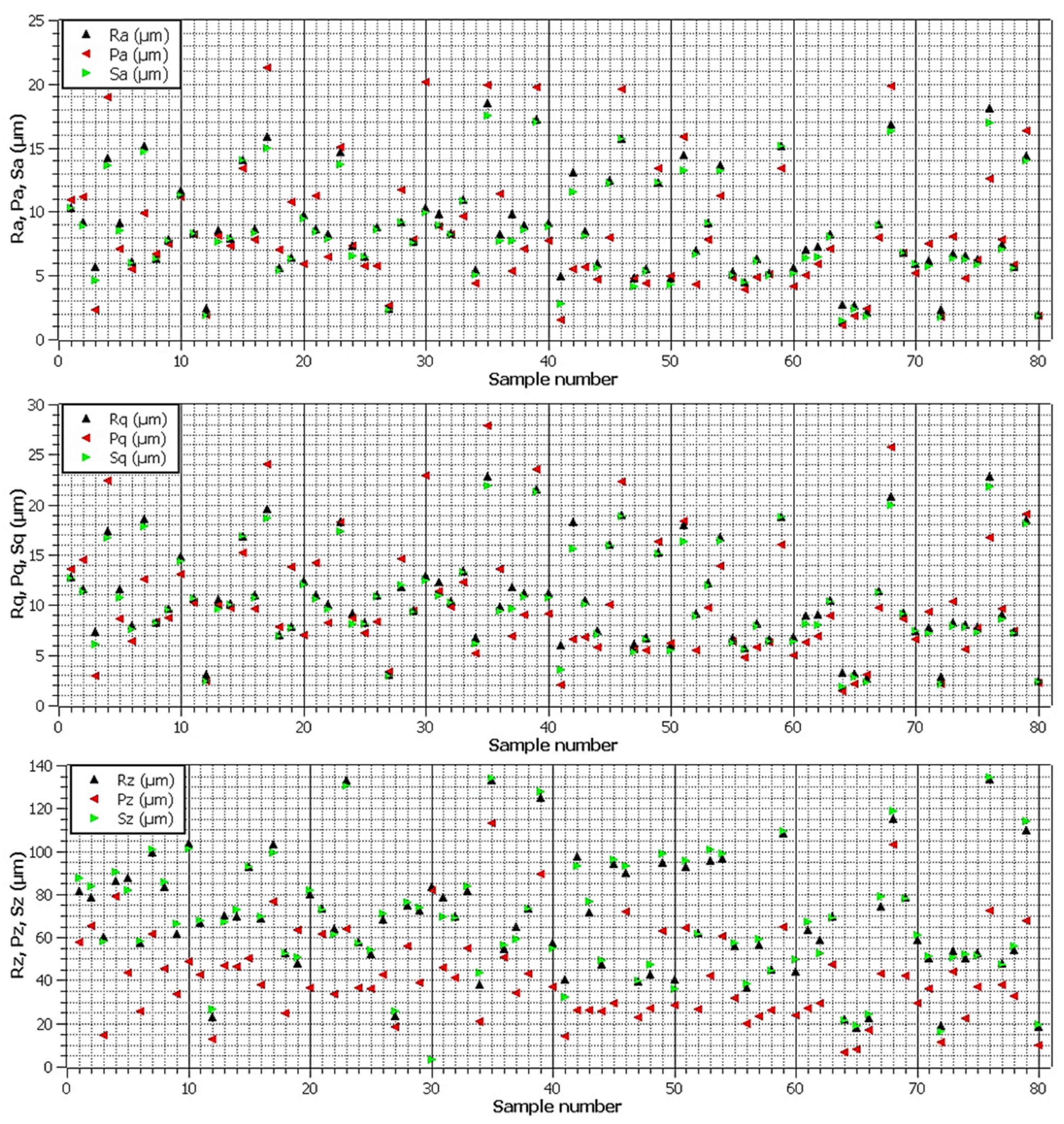
3.2. Surface Topography

The quality of machined surfaces is traditionally at the center of industrial production. Its correct measurement, evaluation of suitable parameters and, last but not least, a correct interpretation of the measured data makes it possible to predict not only the service life of the component, but especially its correct functionality. Whatever production method was used to create the surface on the measured surface, it will always leave some marks (i.e., surface texture). Surface texture (i.e., a three-dimensional set of repeated and random deviations from the microgeometry of the surface of the machined area) has a fundamental influence on the correct functioning of the area, respectively, entire components. The texture of the surface directly affects the quality of the product, so it is necessary to define it as best as possible to predict the behavior and properties of the surface during its operation.
The analysis of the surface topography concerning the setting of the machine parameters is therefore necessary, especially in cases where the part is machined only by EDM without a subsequent finishing technology, usually in the form of grinding. For this reason, three basic profile parameters, three profile parameters, and three area equivalents were evaluated in this experiment to ensure a quantitative evaluation of the area in all technically significant directions [20]. The evaluated parameters of the basic profile were the average height of profile (Pa), mean peak to valley height of the primary profile (Pz), and root mean square height of profile (Pq). The parameters evaluated by the profile method were arithmetical mean deviation of profile (Ra), a maximum height of profile (Rz), and root mean square deviation (Rq). By the area method, the following parameters were evaluated: arithmetical mean height (Sa), maximum surface height (Sz), and root mean square height (Sq). All parameters were evaluated using the Dektak XT contact 3D profilometer supplied by Bruker according to the corresponding standard for area parameters ISO 25178-2 [26] and profile ISO 4287 [27]. Five random spots on each sample were selected for the measurement, and subsequently, the average of these values was obtained.
The evaluated surface topography parameters of the individual samples were compiled into the graphs shown in Figure 2. Since the machining of two different materials was tested during the experiment, a total of four samples were selected with two different tool electrode shapes, in which the lowest values of almost all topography parameters were evaluated. For the samples made of 1.2363 steel, the best evaluated were Samples 64 (electrode material: copper, electrode shape 100 mm × 100 mm) and 66 (electrode material: graphite, electrode shape 10 mm × 10 mm), with the Ra value for Sample 64 being only 2.6 µm, and for Sample 66, the value of Ra was 2.1 µm. The samples made of 1.2343ESR steel had the lowest parameters of almost all topography parameters for Samples 65 (electrode material: graphite, electrode shape 100 mm × 100 mm) and 80 (electrode material: graphite, electrode shape 10 mm × 10 mm). The Ra parameter for Sample 65 was 2.6 µm and the value for Sample 80 was 1.9 µm. From the evaluated values, it is evident that lower surface topography values were achieved when machining by a 10 mm × 10 mm electrode, which corresponded to the Lee study [28], where it was also found that a smaller electrode size is more suitable for obtaining a higher surface quality.
To illustrate the relief of the machined surfaces, a 3D scan of the surfaces of Samples 64 (electrode material: copper) and 65 (electrode material: graphite) with the highest surface finish machined with an electrode of 100 mm × 100 mm was created on the Dektak XT device. This 3D scan was then processed in the Gwyddion program. Both of these 3D reliefs are shown in Figure 3, where a typical EDM surface consisting of a large number of individual craters and depressions is well depicted.

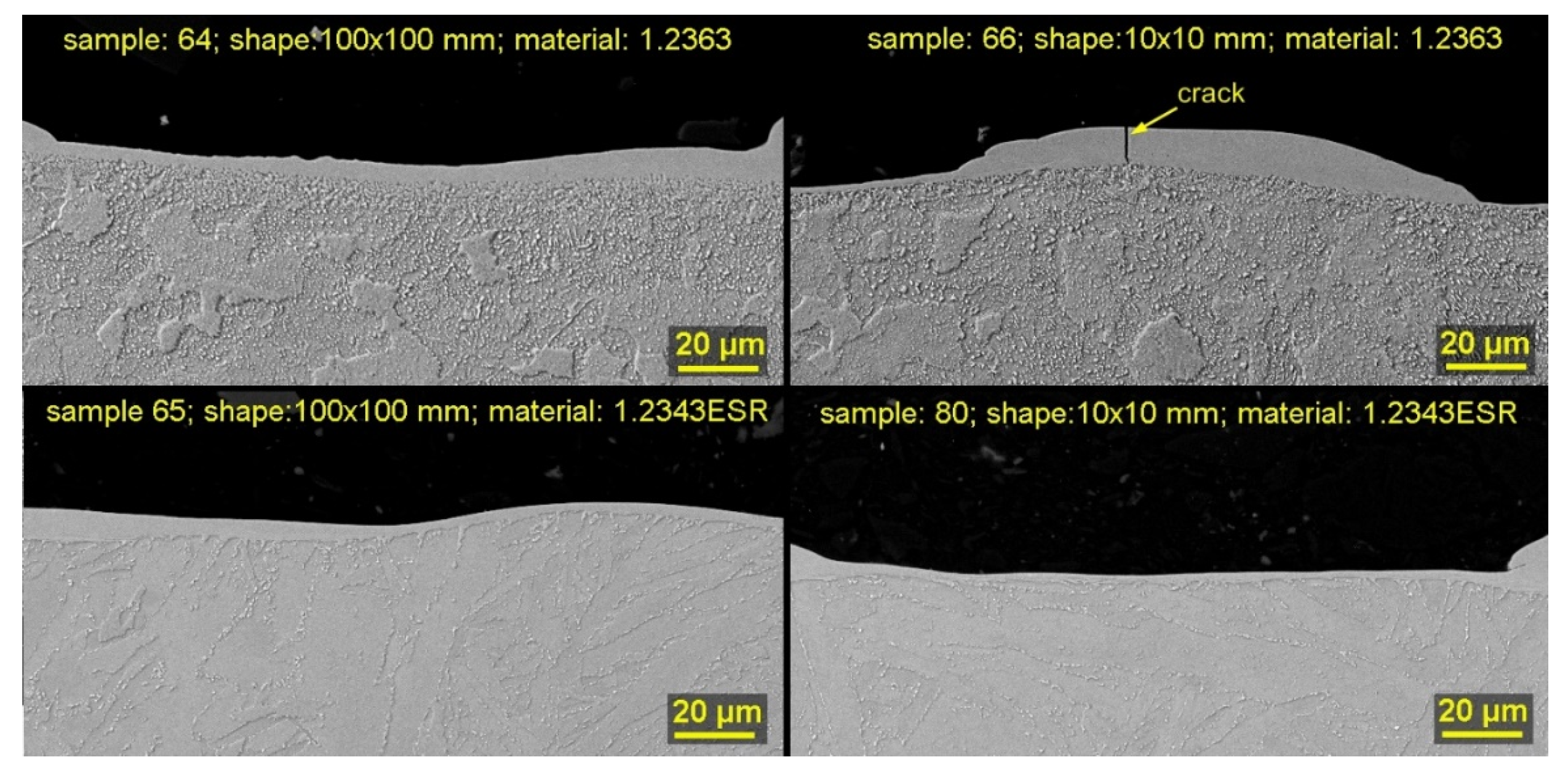
3.3. The Morphology Analysis of the Surface and Subsurface Area Including Defects

Due to the effect of individual electric discharges, a large number of craters are formed on the electrical discharge machined surface. However, these craters are relatively irregularly spaced, and their size and appearance vary due to a large number of input factors, which are not only different material types and heat treatment [29], but also machine parameter settings [30], the type and size of the electrode used [31], or the state of the dielectric [32].
The surface morphology of all machined samples was studied by electron microscopy. In all cases, a secondary electron (SE) detector was used for imaging, with the samples always studied at a magnification of 150×, 500×, and subsequently 1000×.
The morphology appearance of individual samples was very different and closely correlated with the previous surface topography analysis. The only thing that could not be detected in the analysis of the topography was the occurrence of cracks and could only be examined and assessed in this way of analysis. Figure 4 shows the morphology and analysis of the chemical composition of four samples (64, 65, 66, and 80), which had the lowest values of the topography parameters with respect to the electrode size (10 mm × 10 mm or 100 mm × 100 mm) and the workpiece material (1.2363 or 1.2343ESR steel). The images show that all surfaces were relatively smooth, without significant craters, which was also observed from the point of view of the topography. Based on the analysis of the chemical composition, it can be said that there was no significant diffusion from the tool electrode. Samples 65, 66, and 80 were machined with a graphite electrode and the percentage of carbon in these samples was only an average of 1.5 wt.% higher than that of Sample 64, which was machined with a copper electrode. Additionally, no copper was found on this sample, so it cannot be unequivocally said that in graphite electrode treated samples, the increased percentage of carbon was not caused by environmental contamination.
The next step in the analysis of the morphology of machined surfaces was the study of defects: cracks. The occurrence of defects is a binary variable and its modelling uses a binary logistic regression, which predicts the probability of occurrence of the selected binary level, in our case, the occurrence of defects. Binary logistic regression describes the probability of the occurrence of the observed binary symbol. Depending on the observed predictors, these predictors can be both numerical and categorical. The basis of this model is classical linear regression, where the response is the natural logarithm of the chance of the observed phenomenon, where the chance of the events is the probability that the event will occur, to the probability that the event will not occur. This model is described in detail in Agresti [16]. The occurrence of defects on individual samples is shown in Table 3. Minitab 17 was used to calculate the model. From the logistic regression output, it is obvious that the factors open-voltage, pulse current, pulse on time, and Shape * Electrode interaction are statistically significant (p-value < 0.05). The regression equations describing the probability of occurrence of defects are as follows:
P(yes) = exp(Y’)/(1 + exp(Y’)); Shape = 100 × 100, Electrode = graphite
Y’ = 2.102 + 0.01440U − 0.1583I + 0.02379Ton; Shape = 100 × 100, Electrode = copper
Y’ = 3.480 + 0.01440U − 0.1583I + 0.02379Ton; Shape = 10 × 10, Electrode = graphite
Y’ = 3.480 + 0.01440U − 0.1583I + 0.02379Ton; Shape = 10 × 10, Electrode = copper
Y’ = 2.102 + 0.01440U − 0.1583I + 0.02379Ton
where P is the probability and Y’ is the substitution.
Equations (1)–(5) describe the probability of occurrence of defects relative to input variables. Since there are two categorical input variables of two levels, four equations should be given, one for each level combination. The effect of individual factors on the probability of defects is apparent from Figure 5a, wherein the Workpiece material is marked by 1 (1.2363 steel) and 2 (1.2343ESR steel). It can be seen that the incidence of defects decreased with increasing pulse current and decreasing open-voltage and pulse ontime. Shape and Electrode were included in the model because of the significant Shape * Electrode interaction, although they were statistically insignificant. The interaction itself is shown in Figure 5b and it is clear that to minimize the number of defects, large electrodes of 100 mm × 100 mm should be made of copper and small electrodes of 10 mm × 10 mm of graphite. Contour plots for the probability of a defect are shown in Figure 5c.
The analysis of the subsurface layer is crucial due to the frequent occurrence of subsurface defects in the form of cracks (Guu [33], Lee [34], or Kumar [35]) that affect the correct functionality and predicted life of the manufactured component. These cracks may only be within the recast layer or may interfere with the base material. The analysis was performed using electron microscopy on the pre-prepared metallographic preparations of all samples. A back-scattered electrons (BSE) detector was used throughout the whole analysis, first with a magnification of 1000×, and then with a magnification of 2500× and 4000×.
A cross-section of the samples illustrating the state of their subsurface layer is shown in Figure 6. These four samples achieved the best surface quality in terms of topography, however, Sample 66 had small micro-cracks on its surface, but they did not interfere with the base material. No cracks were found in any of the 80 samples of the whole experiment, which would interfere with the base material and thereby disrupt it (i.e., all the cracks described in Table 3 were only within the recast layer). All samples had a continuous recast layer with a thickness of 2–3 µm up to 30 µm. The continuous recast layer is very typical of steels, as was confirmed by Wang [36].

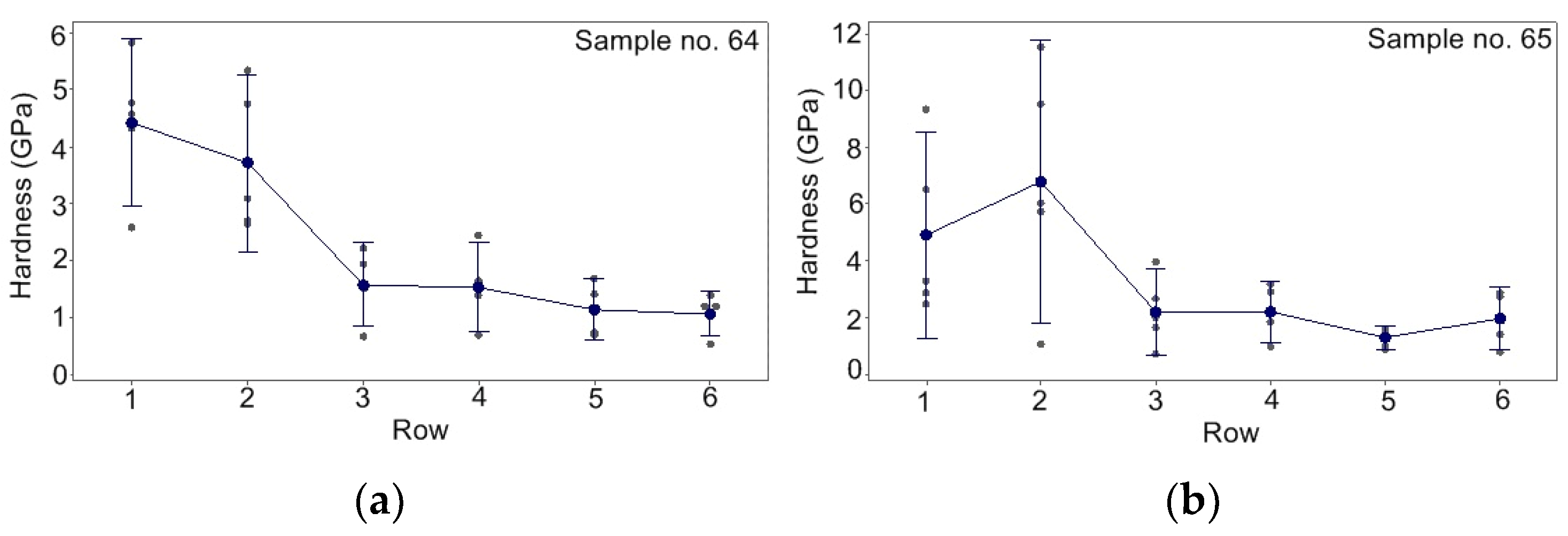
3.4. The Hardness Analysis of a Subsurface Layer

The nanoindentation method on a Hysitron TI 950 Triboindenter (Bruker, Billerica, MA, USA) equipped with a 50 nm Berkovič tip was used to determine the change in the hardness of the subsurface area due to EDM effects. The load was measured according to the standard trapezoid function with a force of 8 mN. Thirty nanoindentation measurements were performed, arranged in a 5 × 6 matrix, to a total depth of 24 µm below the surface of the sticker. The distance between the indents in the x-axis was 5 and 4 µm in the y-axis. The hardness change measurements were performed on Samples 64 (steel: 1.2363, electrode material: copper, electrode shape 100 mm × 100 mm) and 65 (steel: 1.2343ESR, electrode material: graphite, electrode shape 100 mm × 100 mm) due to their highest surface quality without cracking occurrence. Point and interval estimates with the confidence of 95% of medium hardness value for each series are shown in Figure 7.
The graph in Figure 7a shows that in Sample 64, there was a significant change in hardness between Rows 2 and 3, spaced 8 and 12 µm away from the surface, then due to the increasing distance, there was a gradual decrease in the hardness values. A similar significant decrease could be seen in Sample 65. The only significant difference was the initial increase in hardness between Rows 1 and 2, followed by a significant decrease in Row 3. The change in hardness of both samples indicates the hardening of the workpiece material after EDM, and a similar change in hardness affected by EDM has been reported by several scientific groups, for example, in the machining of aluminum [37] or Ti–6Al–4V [38]. On the other hand, some other types of steel such as SKD61 [39] or AISI H13 [40] had become brittle. The change in hardness during EDM machining, therefore, depends on the type of material to be machined and the setting of the machining parameters.

3.5. TEM Lamella Analysis

For a detailed study of the recast layer area, two lamellae were produced for observation under a transmission electron microscope from Samples 64 (steel: 1.2363, electrode material: copper, electrode shape 100 mm × 100 mm) and 65 (steel: 1.2343ESR, electrode material: graphite, electrode shape 100 mm × 100 mm) using a focused ion beam (FIB), which was part of the HELIOS electron microscope. The EDX analysis of both lamellae was performed with an accelerating voltage of 300 kV in scan mode. The beam current during the measurement was set to 1 nA, which provided an optimal detection signal. An image of the entire lamella from Sample 64 is shown in Figure 8, with three details selected in which EDX analysis was performed. Figure 8 shows that there were grains in the material under research with a higher content of alloying elements. Silicon with molybdenum formed one type of grain and the other consisted of chromium, manganese, vanadium, and carbon. Furthermore, vanadium formed small localized grains. The occurrence of copper on the surface of the sample came from the lamella manufacturing process, during which the copper holder material was transferred during the dust removal. The exact chemical composition in detail is compiled in Table 4, where atomic fraction (%) indicates the total proportion of atoms of a given element in the measurement area and fit error (%) indicates the percentage measurement errors. Figure 8 shows that the first third of the lamella (6 µm from above) of the so-called recast layer was mainly made up of iron with a higher occurrence of chromium and carbon. The other elements had a very low concentration in the area. In addition to the increased amount of chromium in the recast layer, there was also a slightly higher amount of molybdenum, manganese, and carbon. Comparing the data in Table 4 in Detail 1 and 2, it is apparent that there was a slight decrease in the total amount of alloying elements locally, which was compensated locally by a higher amount of iron. A change in the concentration of alloying elements and iron was also observed in other materials, for example, there was a localized decrease in iron in the adherent part in AISI 304 steel [41].
It can be seen from Detail 3 that molybdenum was the dominant element in the first type of grains composed of molybdenum and silicon. In the second type of grains, the chromium content prevailed over vanadium, carbon, and manganese. Comparison of the chemical composition in Details 1 and 3 showed that locally, there was a significant decrease in the amount of iron by 5.5%, which was compensated by the increase in other elements up to manganese. The highest overall increase occurred in molybdenum, which was over 90%.
The lamella produced from Sample 65 is shown in Figure 9, wherein the EDX measurement in Detail 1 showed that the grains in the material to be examined consisted mainly of chromium with a small amount of vanadium, manganese, and molybdenum. As with Sample 64, vanadium formed small lone grains. An increased amount of alloying elements accompanied by a lower iron content was detected in the recast layer area. A significant increase in the amount of carbon at the top of the lamella was due to the protective carbon layer used in production. As a standard, other materials such as platinum or tungsten were used as a protective layer in the lamella production, but carbon had to be used due to previous unsuccessful attempts to manufacture the lamella from Sample 65 with the tungsten protective layer. Another possible explanation would be the transfer of carbon from the electrode to the workpiece. A diffusion of material from the EDM electrode is a well-known phenomenon, which is well described in the available literature [42,43,44]. The chemical composition in Detail 1 was summarized in Table 5. The occurrence of copper in the material under investigation can again be explained by the secondary transfer of the lamella holder material during dust removal.
The EDX measurement in Detail 2 focused more closely on the recast layer area, however, due to an error during the measurement, the scan of the measured area was not interleaved with the TEM image. The EDX analysis clearly showed that due to EDM, there was an increased concentration of individual alloying elements in the upper part, except for molybdenum, which was compensated by a decrease in the iron content. The comparison of EDX analysis data from Details 1 and 2 showed that locally, there was a significant increase in carbon and a slight increase in vanadium content. Other elements showed a slight decrease. The last EDX measurement in Detail 3 was focused on the composition of individual grains, while the image clearly showed that the main component of the displayed grains consisted mainly of chromium. The other alloying elements in these grains also showed an increased content, except for silicon, and it was also possible to see a separate vanadium grain. From the comparison of the data of Details 3 and 1, it is evident that in the investigated area, the vanadium content was doubled, there was a 20% increase in chromium, and a slight increase in the silicon and molybdenum values.

4. Conclusions

Based on the designed 80-round experiment, extensive research on EDM was carried out taking into account not only four different machine setting parameters, but also two different types of tool electrode materials (graphite and copper), electrode shape (10 mm × 10 mm and 100 mm × 100 mm), and two different types of the machined material, 1.2363 and 1.2343ESR steel. Based on the many analyses carried out, the following conclusions were reached:
The best surface topography of the sample made of 1.2363 steel was Sample 66, which was made with the parameter settings of U = 220 V, I = 20 A, Ton = 100 µs, Toff = 80 µs with a 10 mm × 10 mm graphite electrode and a Ra of only 2.1 µm, and at the same time, Sample 80 made of 1.2343ESR steel, which was produced by the same machine parameter setting with the same electrode and had the lowest value of the parameter R of only 1.9 µm.
  • The morphology of the individual samples was very different and closely correlated with the surface topography analysis, with cracks being studied on some samples, that were further assessed cross-sectioned and statistically analyzed for their occurrence.
  • The cross-section analysis of all samples showed cracks in some samples, but these were always in the recast layer only and did not interfere with the base material.
  • The occurrence of defects was modelled using binary logistic regression, which made it possible to predict the probability of the occurrence of defects on the surface of samples based on input variables and to create regression equations describing the probability of crack occurrence.
  • Based on the measurement of the local hardness development in the subsurface layer of the samples, hardening of the material after EDM was found, but only to a depth of 8–12 µm, with no further impact on the material; and
  • The TEM lamellae produced allowed for a detailed study of the microstructure of materials and their changes caused by a die-sinking EDM.
Based on the above conclusions of the individual analyses, it can be clearly stated that it is possible to effectively predict the probability of cracking on machined surfaces and also in machine 1.2363 and 1.2343ESR steels with a very good surface quality with Ra 1.9 and 2.1 µm using graphite electrodes. These findings will ensure the production of parts with the required surface quality without cracks, which is a crucial aspect for maintaining the required functionality and service life of the parts.

Author Contributions

Conceptualization, K.M. and R.Z.; Methodology, J.B. and K.M.; Software, J.B. and T.P.; Validation, K.M., J.F. and L.B.; Formal analysis, K.M. and R.Z.; Investigation, K.M., J.B., and L.B.; Resources, R.Z. and T.P.; Data curation, L.B.; Writing—original draft preparation, K.M. and R.Z.; Writing—review and editing, K.M.; Visualization, K.M.; Supervision, K.M.; Project administration, L.B.; Funding acquisition, L.B. and K.M. All authors have read and agreed to the published version of the manuscript.

Funding

This work was supported through Project No. LO1207 and Technology Agency of the Czech Republic, Project No. TJ02000311.

Acknowledgments

Part of the work was carried out with the support (ID LM2018110, MEYS CR) and “Modern mathematical methods for modeling problems of technical and natural sciences”, FSI−S−17−4464.

Conflicts of Interest

The authors declare no conflicts of interest.

References

  1. McGeough, J.A. Advanced Methods of Machining; Springer Science & Business Media: New York, NY, USA, 1988. [Google Scholar]
  2. Ho, K.H.; Newman, S.T. State of the art electrical discharge machining (EDM). Int. J. Mach. Tools Manuf. 2003, 43, 1287–1300. [Google Scholar] [CrossRef]
  3. Garg, R.K.; Singh, K.K.; Sachdeva, A.; Sharma, V.S.; Ojha, K.; Singh, S. Review of research work in sinking EDM and WEDM on metal matrix composite materials. Int. J. Adv. Manuf. Technol. 2010, 50, 611–624. [Google Scholar] [CrossRef]
  4. Muthuramalingam, T.; Mohan, B. A review on influence of electrical process parameters in EDM process. Arch. Civ. Mech. Eng. 2015, 15, 87–94. [Google Scholar] [CrossRef]
  5. Meshram, D.B.; Puri, Y.M. Review of research work in die sinking EDM for machining curved hole. J. Braz. Soc. Mech. Sci. Eng. 2017, 39, 2593–2605. [Google Scholar] [CrossRef]
  6. Nikalje, A.M.; Kumar, A.; Srinadh, K.S. Influence of parameters and optimization of EDM performance measures on MDN 300 steel using Taguchi method. Int. J. Adv. Manuf. Technol. 2013, 69, 41–49. [Google Scholar] [CrossRef]
  7. Rajendran, S.; Marimuthu, K.; Sakthivel, M. Study of crack formation and resolidified layer in EDM process on T90Mn2W50Cr45 tool steel. Mat. Manuf. Proc. 2013, 28, 664–669. [Google Scholar]
  8. Majumder, A. Process parameter optimization during EDM of AISI 316 LN stainless steel by using fuzzy based multi-objective PSO. J. Mech. Sci. Technol. 2013, 27, 2143–2151. [Google Scholar] [CrossRef]
  9. Gill, A.S.; Kumar, S. Surface alloying of H11 die steel by tungsten using EDM process. Int. J. Adv. Manuf. Technol. 2015, 78, 1585–1593. [Google Scholar] [CrossRef]
  10. Corný, I.; Pitel, J.; Hašová, S. Statistical approach to optimize the process parameters of HAZ of tool steel EN X32CrMoV12-28 after die-sinking EDM with SF-Cu electrode. Metals 2017, 7, 35. [Google Scholar]
  11. Santos, R.F.; Silva, E.R.; Sales, W.F.; Raslan, A.A. Analysis of the surface integrity when nitriding AISI 4140 steel by the sink electrical discharge machining (EDM) process. Procedia CIRP 2016, 45, 303–306. [Google Scholar] [CrossRef] [Green Version]
  12. Sidhom, H.; Ghanem, F.; Amadou, T.; Gonzalez, G.; Braham, C. Effect of electro discharge machining (EDM) on the AISI316L SS white layer microstructure and corrosion resistance. Int. J. Adv. Manuf. Technol. 2013, 65, 141–153. [Google Scholar] [CrossRef] [Green Version]
  13. Dewangan, S.; Gangopadhyay, S.; Biswas, C.K. Multi-response optimization of surface integrity characteristics of EDM process using grey-fuzzy logic-based hybrid approach. Eng. Sci. Technol. Int. J. 2015, 18, 361–368. [Google Scholar] [CrossRef] [Green Version]
  14. Dewangan, S.; Biswas, C.K.; Gangopadhyay, S. Influence of different tool electrode materials on EDMed surface integrity of AISI P20 tool steel. Mat. Manuf. Proc. 2014, 29, 1387–1394. [Google Scholar] [CrossRef]
  15. D’Urso, G.; Giardini, C.; Quarto, M. Characterization of surfaces obtained by micro-EDM milling on steel and ceramic components. Int. J. Adv. Manuf. Technol. 2018, 97, 2077–2085. [Google Scholar] [CrossRef]
  16. Valentinčič, J.; Kušer, D.; Smrkolj, S.; Blatnik, O.; Junkar, M. Machining parameters selection for varying surface in EDM. Int. J. Mat. Prod. Technol. 2007, 29, 344. [Google Scholar] [CrossRef] [Green Version]
  17. Debnath, T.; Baroi, B.K.; Patowari, P.K. Machinability study of 430 stainless steel using tap water in EDM. Mater. Today Proc. 2020. [Google Scholar] [CrossRef]
  18. Jarosz, K.; Nieslony, P.; Löschner, P. Investigation of the effect of process parameters on surface roughness in EDM machining of ORVAR® supreme die steel. In Advances in Manufacturing Engineering and Materials; Springer: Cham, Switzerland, 2019; pp. 333–340. [Google Scholar]
  19. Valarmathi, T.N.; Sekar, S.; Anthony, G.; Suresh, R.; Balan, K.N. Experimental studies on surface roughness of H12 tool steel in EDM using different tool materials. In Innovative Design, Analysis and Development Practices in Aerospace and Automotive Engineering (I-DAD 2018); Springer: Singapore, 2019; pp. 241–247. [Google Scholar]
  20. Jiang, X.J.; Whitehouse, D.J. Technological shifts in surface metrology. CIRP Ann. Manuf. Technol. 2012, 61, 815–836. [Google Scholar] [CrossRef]
  21. Mouralova, K.; Klakurkova, L.; Matousek, R.; Prokes, T.; Hrdy, R.; Kana, V. Influence of the cut direction through the semi-finished product on the occurrence of cracks for X210Cr12 steel using WEDM. Arch. Civ. Mech. Eng. 2018, 18, 1318–1331. [Google Scholar] [CrossRef]
  22. Mouralova, K.; Benes, L.; Bednar, J.; Zahradnicek, R.; Prokes, T.; Matousek, R.; Fiserova, Z.; Otoupalik, J. Using a DoE for a comprehensive analysis of the surface quality and cutting speed in WED-machined hadfield steel. J. Mech. Sci. Technol. 2019, 33, 2371–2386. [Google Scholar] [CrossRef]
  23. Mouralova, K.; Prokes, T.; Benes, L.; Sliwkova, P. Analysis of subsurface defects occurrence in abrasion resistant Creusabro steel after WEDM including the study of morphology and surface topography. Mach. Sci. Technol. 2020, 24, 274–290. [Google Scholar] [CrossRef]
  24. Mouralova, K.; Prokes, T.; Benes, L.; Bednar, J. The influence of WEDM parameters setup on the occurrence of defects when machining hardox 400 steel. Materials 2019, 12, 3758. [Google Scholar] [CrossRef] [Green Version]
  25. Mouralova, K.; Prokes, T.; Benes, L. Surface and subsurface layers defects analysis after WEDM affecting the subsequent lifetime of produced components. Arab. J. Sci. Eng. 2019, 44, 7723–7735. [Google Scholar] [CrossRef]
  26. Geometrical Product Specifications (GPS). Surface Texture: Areal. Part 2: Terms, Definitions and Surface Texture Parameters; ISO 25178-2; International Organization for Standardization: Geneva, Switzerland, 2012. [Google Scholar]
  27. Geometrical Product Specifications (GPS). Surface Texture: Profile Method. Terms, Definitions and Surface Texture Parameters; ISO 4287; International Organization for Standardization: Geneva, Switzerland, 1997. [Google Scholar]
  28. Lee, H.T.; Rehbach, W.P.; Tai, T.Y.; Hsu, F.C. Relationship between electrode size and surface cracking in the EDM machining process. J. Mater. Sci. 2004, 39, 6981–6986. [Google Scholar] [CrossRef]
  29. Ekmekci, B. White layer composition, heat treatment, and crack formation in electric discharge machining process. Metall. Mater. Trans. B 2009, 40, 70–81. [Google Scholar] [CrossRef]
  30. Keskin, Y.; Halkacı, H.S.; Kizil, M. An experimental study for determination of the effects of machining parameters on surface roughness in electrical discharge machining (EDM). Int. J. Adv. Manuf. Technol. 2006, 28, 1118–1121. [Google Scholar] [CrossRef]
  31. Liu, Q.; Zhang, Q.; Zhu, G.; Wang, K.; Zhang, J.; Dong, C. Effect of electrode size on the performances of micro-EDM. Mater. Manuf. Proc. 2016, 31, 391–396. [Google Scholar] [CrossRef]
  32. Yan, B.H.; Tsai, H.C.; Huang, F.Y. The effect in EDM of a dielectric of a urea solution in water on modifying the surface of titanium. Int. J. Mach. Tools Manuf. 2005, 45, 194–200. [Google Scholar] [CrossRef]
  33. Guu, Y.H. AFM surface imaging of AISI D2 tool steel machined by the EDM process. Appl. Surf. Sci. 2005, 242, 245–250. [Google Scholar] [CrossRef]
  34. Lee, S.H.; Li, X. Study of the surface integrity of the machined workpiece in the EDM of tungsten carbide. J. Mat. Proc. Technol. 2003, 139, 315–321. [Google Scholar] [CrossRef]
  35. Kumar, K.L.; Rao, C.S.; Sateesh, B.; Viswanath, M.S.R. Analysis of Micro-cracks and Micro-hardness in White Layer Formation on Machined Surfaces in EDM Process. In Advances in Applied Mechanical Engineering; Springer: Singapore, 2020; pp. 955–963. [Google Scholar]
  36. Wang, C.C.; Chow, H.M.; Yang, L.D.; Lu, C.T. Recast layer removal after electrical discharge machining via Taguchi analysis: A feasibility study. J. Mater. Proc. Technol. 2009, 209, 4134–4140. [Google Scholar] [CrossRef]
  37. Mahdieh, M.S.; Mahdavinejad, R. Recast layer and micro-cracks in electrical discharge machining of ultra-fine-grained aluminum. Proc. Inst. Mech. Eng. Part B J. Eng. Manuf. 2018, 232, 428–437. [Google Scholar] [CrossRef]
  38. Muttamara, A. Comparison performances of EDM on Ti6Al4V with two graphite grades. Int. J. Chem. Eng. Appl. 2015, 6, 250–253. [Google Scholar] [CrossRef] [Green Version]
  39. Phan, N.H. Analysis of surface layers of hot–forging dies of SKD61 steel fabricated by die–sinking electrical discharge machining using copper and titanium electrodes. Vietnam J. Sci. Technol. 2016, 54, 19–26. [Google Scholar] [CrossRef]
  40. Matin, R.; Rahmani, R.; Shabgard, M.R. Effect of input parameters on the depth of heat affected zone (HAZ) AISI H13 steel electrical discharge machining process (EDM). Int. J. Mater. Eng. Technol. 2019, 2, 33–38. [Google Scholar]
  41. Abu Qudeiri, J.E.; Saleh, A.; Ziout, A.; Mourad, A.H.I.; Abidi, M.H.; Elkaseer, A. Advanced electric discharge machining of stainless steels: Assessment of the state of the art, gaps and future prospect. Materials 2019, 12, 907. [Google Scholar] [CrossRef] [Green Version]
  42. Kumar, S.; Singh, R.; Singh, T.P.; Sethi, B.L. Comparison of material transfer in electrical discharge machining of AISI H13 die steel. Proc. Inst. Mech. Eng. C J. Mech. Eng. Sci. 2009, 223, 1733–1740. [Google Scholar] [CrossRef]
  43. Mandal, P.; Mondal, S.C. Surface characteristics of mild steel using EDM with Cu-MWCNT composite electrode. Mater. Manuf. Proc. 2019, 34, 1326–1332. [Google Scholar] [CrossRef]
  44. Stráský, J.; Janeček, M.; Harcuba, P.; Bukovina, M.; Wagner, L. The effect of microstructure on fatigue performance of Ti–6Al–4V alloy after EDM surface treatment for application in orthopaedics. J. Mech. Behav. Biomed. Mater. 2011, 4, 1955–1962. [Google Scholar] [CrossRef]
Figure 1. (a) Eroding process, (b) samples produced, (c) microstructure representation and chemical composition analysis of 1.2363 steel, (d) microstructure representation and chemical composition analysis of 1.2343ESR steel.
Coatings 10 00406 g001
Figure 2. Basic profile parameters, profile, and area parameters of individual experimental samples.
Coatings 10 00406 g002
Figure 3. Color filtered relief of the sample surface machined by a 100 mm × 100 mm electrode. (a) Sample 64 (electrode material: copper), (b) Sample 65 (electrode material: graphite).
Coatings 10 00406 g003
Figure 4. Morphology of the scanning electron microscopy (SEM) samples (SE) including chemical composition analysis.
Coatings 10 00406 g004
Figure 5. (a) diagram of the main defect probability effects; (b) Diagram of the defect probability interactions; (c) Contour probability contour plots.
Coatings 10 00406 g005
Figure 6. Showing the state of the subsurface sample layer and defects, SEM (BSE).
Coatings 10 00406 g006
Figure 7. Development of local hardness (95% confidence interval) as a function of distance from the sample surface (individual standard deviations are used to calculate the intervals): (a) Sample 64; (b) Sample 65.
Coatings 10 00406 g007
Figure 8. Lamella of Sample 64 of 1.2363 steel (electrode material: copper, electrode shape 100 mm × 100 mm) together with three different details where the chemical composition analysis was performed.
Coatings 10 00406 g008
Figure 9. Lamella of Sample 65 of steel 1.2343ESR (electrode material: graphite, electrode shape 100 mm × 100 mm) together with three different details where the chemical composition analysis was performed.
Coatings 10 00406 g009
Table 1. Values of the input parameters for the design of experiments.
ParameterShape of ElectrodeMaterial of ElectrodeMaterial of WorkpieceOpen-Voltage (V)Pulse Current (A)Pulse On
Time (µs)
Pulse Off
Time (µs)
Lower level10 × 10copper1.2363 (1)160105035
Central level22020100 *80 *
Higher level100 × 100graphite1.2343ESR (2)28030200150
* The last two numeric parameters do not behave linearly, so the centers have been shifted.
Table 2. Machining parameters used for individual runs of the experiment.
Sample NumberShape of ElectrodeMaterial of ElectrodeMaterial of WorkpieceOpen-Voltage (V)Pulse Current (A)Pulse on Time (µs)Pulse off Time (µs)
110 × 10graphite12202010080
2100 × 100copper1280305035
3100 × 100graphite1280105035
410 × 10graphite22803020035
5100 × 100graphite12803020035
610 × 10graphite21601050150
7100 × 100copper11603050150
810 × 10graphite116010200150
910 × 10copper11601020035
1010 × 10copper12202010080
11100 × 100copper22803050150
1210 × 10copper12202010080
1310 × 10graphite2160305035
14100 × 100copper12202010080
1510 × 10copper228030200150
16100 × 100graphite22202010080
1710 × 10copper116030200150
1810 × 10copper1280105035
1910 × 10copper22801050150
20100 × 100copper22202010080
21100 × 100graphite12202010080
2210 × 10copper216010200150
2310 × 10graphite216030200150
24100 × 100graphite22801020035
25100 × 100graphite21603050150
26100 × 100copper2160305035
27100 × 100copper22202010080
28100 × 100graphite11601020035
2910 × 10graphite12801020035
3010 × 10copper1160305035
31100 × 100copper116010200150
3210 × 10copper22801020035
3310 × 10graphite22202010080
3410 × 10graphite1160105035
35100 × 100copper128030200150
36100 × 100copper228010200150
3710 × 10graphite1280305035
3810 × 10copper2280305035
3910 × 10copper21603020035
4010 × 10copper128010200150
41100 × 100graphite12202010080
4210 × 10copper12803020035
43100 × 100graphite128010200150
44100 × 100copper1160105035
45100 × 100graphite21603020035
46100 × 100copper216030200150
47100 × 100graphite22801050150
4810 × 10graphite12801050150
4910 × 10copper22202010080
50100 × 100graphite2160105035
51100 × 100graphite228030200150
52100 × 100graphite1160305035
5310 × 10copper12803050150
5410 × 10graphite128030200150
55100 × 100graphite11601050150
5610 × 10graphite2280105035
5710 × x10graphite21601020035
58100 × 100graphite2280305035
59100 × 100graphite116030200150
60100 × 100copper12801050150
61100 × 100graphite12803050150
62100 × 100copper12801020035
6310 × 10graphite22803050150
64100 × 100copper12202010080
65100 × 100graphite22202010080
6610 × 10graphite12202010080
6710 × 10copper21603050150
68100 × 100copper22803020035
6910 × 10graphite11603050150
7010 × 10copper11601050150
71100 × 100copper2280105035
7210 × 10copper22202010080
73100 × 100graphite216010200150
7410 × 10graphite228010200150
75100 × 100copper21601050150
76100 × 100copper11603020035
77100 × 100copper21601020035
7810 × 10copper2160105035
7910 × 10graphite11603020035
8010 × 10graphite22202010080
Table 3. Analysis of defect occurrence on the surface of individual samples.
Sample No.DefectsSample No.DefectsSample No.DefectsSample No.DefectsSample No.Defects
1No17Yes33No49No65No
2No18Yes34Yes50Yes66Yes
3Yes19No35Yes51Yes67No
4No20No36Yes52No68Yes
5Yes21No37No53No69No
6No22Yes38Yes54No70No
7No23No39Yes55No71No
8Yes24Yes40Yes56Yes72No
9Yes25No41Yes57Yes73Yes
10Yes26No42Yes58No74Yes
11No27Yes43Yes59Yes75No
12No28Yes44No60Yes76No
13No29Yes45No61No77Yes
14No30Yes46No62Yes78No
15Yes31Yes47Yes63No79No
16Yes32Yes48Yes64No80No
Table 4. Analysis of the chemical composition in each detail according to Figure 8.
ElementDetail 1Detail 2Detail 3
Atomic Fraction (%)Fit Error (%)Atomic Fraction (%)Fit Error (%)Atomic Fraction (%)Fit Error (%)
C1.740.171.721.642.850.66
Si1.650.271.430.172.050.36
V0.490.130.400.030.690.20
Cr5.650.175.350.217.830.11
Mn0.452.960.462.100.442.91
Fe85.270.0586.350.0579.880.03
Cu4.100.003.730.015.000.02
Mo0.640.310.580.241.260.08
Table 5. Analysis of the chemical composition in each detail according to Figure 9.
ElementDetail 1Detail 2Detail 3
Atomic Fraction (%)Fit Error (%)Atomic Fraction (%)Fit Error (%)Atomic Fraction (%)Fit Error (%)
C3.692.015.960.102.530.73
Si0.560.260.550.260.590.91
V0.090.030.100.160.190.05
Cr4.300.154.000.035.480.27
Mn0.631.450.593.200.582.18
Fe86.230.0884.390.0586.200.12
Cu4.170.024.110.024.090.01
Mo0.330.300.290.090.340.29

