Article

Controlling the Structural, Mechanical and Frictional Properties of MoSx Coatings by High-Power Impulse Magnetron Sputtering

1
Institute of Materials Engineering, TU Dortmund University, Leonhard-Euler-Straße 2, 44227 Dortmund, Germany
2
Experimental Physics 2, TU Dortmund University, Otto-Hahn-Straße 4a, 44227 Dortmund, Germany
3
Chair of Fluidics, TU Dortmund University, Leonhard-Euler-Straße 5, 44227 Dortmund, Germany
*
Author to whom correspondence should be addressed.
Coatings 2020, 10(8), 755; https://doi.org/10.3390/coatings10080755
Submission received: 8 July 2020 / Revised: 24 July 2020 / Accepted: 27 July 2020 / Published: 3 August 2020
(This article belongs to the Special Issue Manufacturing and Surface Engineering II)

Abstract

:
Tribology, as the science and technology of interacting surfaces, typically relies on liquid lubricants which reduce friction and wear. For environmentally friendly tribological purposes and applications requiring a liquid-free performance, solid lubricants, such as MoS2 coatings, play an essential role. It is crucial to understand the interplay between the parameters of the coating synthesis and the characteristics of the coating. The impact of the deposition parameters on the structural, mechanical and frictional properties of MoSx thin films, which are synthesized by high-power impulse magnetron sputtering, are studied. The morphology, topography and stoichiometry (2.02 < x < 2.22) of the films are controlled by, in particular, the bias-voltage and heating power applied during the sputtering process. In combination with a low pulse frequency the hardness and elastic stiffness of the MoSx films are enhanced up to 2 and 90 GPa, respectively. This enhancement is assigned to a shortening of the Mo-S bonding lengths and a strengthening in the interatomic coupling as well as to a formation of small-sized crystallites at the surface. The friction coefficient reduces to µ = 0.10 for films with an initial (100) orientation and the mean roughness of the MoSx films decreases below 15 nm by shortening the cathode pulses.

1. Introduction

Surface modifications of machining parts, subjected to a tribological load, provide the performance and long lifetime which are highly required for today’s production processes and technical applications. Wear resistance and reduced friction are achieved by physical-vapor-deposition (PVD) coatings [1,2]. In this context, the rotor contact in dry-running twin-screw machines without timing gears, examined as prototypes in various application areas, are of special interest [3,4,5]. The rotor mesh is characterized by remarkable tribological requirements taking into account that a lubricating auxiliary fluid is not available. In dry-running operations, a relatively high thermal load occurs in the rotor contact (about 400 °C) underlining the importance of a wear protection coating [6]. In addition to typically used tungsten carbide coatings, a similarly hard diamond-like-carbon wear protection film with a hardness of 15–25 GPa is exploited [7]. The wear rates achieved are promising, but they are still a subject of ongoing research.
In addition to carbon-based hard coatings, lamellar coatings, including graphite, MoS2 and WS2, are successfully used as solid lubricants to reduce the friction coefficient between sliding or rolling surfaces [8,9]. MoS2 features a lamellar buildup in a hexagonal structure with individual molybdenum and sulfur planes, while the molybdenum layer is surrounded by sulfur at both sides. Within the planes covalent bonds and between the planes easily slidable Van-der-Waals bonds are present [10]. For this reason, the different layers can slide against each other and allow low friction coefficients. Since these tribological properties are preserved up to at least 400 °C, these layers find application in various fields [8,11,12].
In contrast to bulk materials, superior properties are achieved using sputtered MoS2 layers. These layers provide low coefficients of friction and a long lifetime compared to films grown by other methods, such as powder-compacted layers [13]. MoS2 layers exhibit a coefficient of friction between µ = 0.15 and 0.30 in conventional air containing at 50% humidity [14]. The coefficient of friction depends on various external parameters, such as the contact pressure, temperature, humidity and layer properties including, for example, the film thickness, growth structure and elastic modulus [8]. The PVD parameters play an essential role for the structural and tribological behavior of MoS2 films.
Important tribological properties, like the friction coefficient, wear resistance and wear particle formation, depend on the composition, adhesion, and morphology or porosity of the interacting surface [15]. A low coefficient of friction and an extended lifetime shall be achieved by combining a good adhesion of the surface layer to the substrate, a high purity of the coating, and a dense morphology with a small crystallite size [15]. For a HiPIMS grown MoSx thin film, a decrease of the friction coefficient is reported with an enhanced surface pressure applied during the tribological contact, due to the formation of more third-body particles leading to a thicker tribofilm formation [16]. A transfer film formation is also promoted by oxygen and H2O in the atmosphere as reported by Li et al. [17].
The growth temperature affects the crystallite size and stoichiometry of the coating: At a temperature of 100 °C, an S/Mo ratio of 1.90 is observed, for direct-current sputtered MoSx films. The ratio further decreases down to 1.71 at about 300 °C, i.e., with increasing substrate temperature [18]. The influence of the bias-voltage on the stoichiometry and structural properties of MoS2-Ti composite films has been studied by Bülbül et al. [19]. With an increasing bias-voltage, the layer thickness and the S/Mo ratio are reduced due to resputtering phenomena and an enhanced ion bombardment. According to Vierneusel et al. [20], the usage of a high bias-voltage leads to a decrease in the friction coefficient, but also to a short coating lifetime. This effect may be ascribed to a high kinetic energy of the species due to the increased bias-voltage. Nevertheless, the diverse impacts of the deposition parameters on the coating properties as well as the corresponding microscopic reasons are not understood in detail yet.
MoS2 thin films have mainly been magnetron-sputtered in the direct-current [18,21] or radio-frequency [20,22,23,24,25,26] mode. To improve the coating properties, MoS2 composite coatings containing TiN [27], or e.g., Ti [19,28], have been grown. Another attempt is the synthesis of a Mo2N/MoS2 composite, merging the unique properties of both materials [29]. Instead of changing the chemical composition, a downstreamed vacuum heat treatment can improve the wear life time of the coating, due to a change from an amorphous-like to a nanocrystal state of the microstructure [30]. A sophisticated growth method is by high-power impulse magnetron sputtering (HiPIMS), which provides a high ionization of the particle plasma by short impulses on the cathode. Films synthesized by HiPIMS reveal a dense and fine morphology [31] leading to a high hardness [32] and a high oxidation resistance [33]. Thus, the tribological properties, like the wear resistance of the film grown by HiPIMS can be improved [34]. Up to now, mainly composite coatings were grown by the HiPIMS method, for example (Cr1-xAlx)N+MoSy [35] and pure MoSx HiPIMS coatings [36,37] have only been rarely studied. For MoSx thin films grown in HiPIMS mode, an increase of the bias-voltage leads to a more pronounced (100) orientation accompanied by an decrease of the friction coefficient [37].
For MoSx films synthesized by the HiPIMS method including the bias-voltage, the impacts of the growth parameters on the structural, mechanical and frictional properties of the films were studied in this research. For comparison, a conventionally direct-current magnetron sputtered MoSx coating was prepared. For correlating the growth parameters with the MoSx film properties and providing microscopic descriptions, complementary characterization methods including scanning electron microscopy, X-ray diffraction, laser light scattering, nanoindentation as well as ball-on-disc tribometer experiments were used. It is demonstrated that the structural inhomogeneity of the dense MoSx films is remarkably affected by the bias-voltage and heating power. An increasing heating power shifts the stoichiometric S/Mo ratio towards 2 which is attributed to a high surface diffusion during the synthetization process. A weak heating power and low pulse frequency lead to a shortening of the Mo-S bonding lengths and to an enhancement in the interatomic coupling as well as to the formation of small-sized crystallites at the surface. As a result, the hardness of the MoSx films rises up to 2 GPa. The friction coefficients of the HiPIMS films range between 0.10 and 0.16. A high coefficient of friction is observed for films with a homogeneous structure which is resistant against shear forces. A low averaged friction coefficient is achieved for films with an initial (100) orientation. Moreover, short pulses cause smooth surfaces of the MoSx coatings with mean roughness values of less than 15 nm. The study provides a major step towards the understanding of the interplay between HiPIMS deposition parameters and the properties of MoSx films, making them a promising platform for the solid lubrication in tribologically relevant applications.

2. Materials and Methods

MoSx thin films were deposited on heat-treated steel substrates (1.2343, AISI-H11) with a hardness of (8.1 ± 0.4) GPa and on (100)-oriented silicon wafers using an unbalanced magnetron sputtering device (CC800/9 Custom, CemeCon AG, Würselen, Germany). The substrates were ground and polished in different steps (9, 6 and 3 µm suspension) prior to the coating process to enhance the surface quality to an arithmetic mean roughness of Ra = (4.9 ± 0.5) nm. After each step, the substrates were cleaned in an ultrasonic ethanol bath. In the PVD chamber, the substrates were heated up and were subjected to a gas-etching process (mixture of argon and krypton gas) which removed oxides from the surface. A subsequent booster-etching process using two molybdenum targets was used to improve the adhesion of the MoSx films on the substrates, as reported for MoS2-Nb composites [38]. The films were deposited by the HiPIMS technique using a MoS2 target of 99.5% purity and an average cathode power of 3 kW. The used target arrangement is shown in Figure 1a.
Argon and krypton were used as process gases leading to a total chamber pressure of 350 mPa. The bias-voltage was synchronized with the HiPIMS cathode by 150-µs-pulses and an offset of 40 µs. The heating power was set to PH = 3 kW, the bias-voltage to UB = −150 V, the pulse frequency to fp = 700 Hz, and the pulse duration to tp = 150 µs. These deposition parameters define the central parameters of our coating design and, in turn, that of sample ID1. For the samples ID2 to ID9, the deposition parameters were changed to lower and higher values in a definite manner so that three different values for each parameter were investigated. An overview of the deposition parameters and structural properties is given in Table 1. A reference MoSx thin film (DC) was sputtered in direct-current mode with deposition parameters corresponding to that of the central sample ID1. For the reference film the bias-voltage was changed from the pulsed to the direct-current mode. For all parameters, the sputtering time was kept constant at 3800 s.
The coatings were designed by means of a predictive analytics software (JMP Pro 14, SAS Institute Inc., Cary, NC, USA). For the statistically based analysis of the parameters and experimental data, linear effects of the deposition parameters on structural and mechanical properties of the MoSx films were taken into account and mutual interactions were neglected. The significance of the analyzed deposition parameters was determined in accordance with a significance level of 0.05 using the probability value (p-value). For evaluating the effects of the deposition parameters, a t-test was performed. The respective values are listed in Table 2. The statistical analysis is based on the following null hypothesis: The deposition parameters (heating power, bias-voltage, pulse frequency and pulse duration) do not affect the properties of the MoSx films.
The voltage and current of the cathode pulses were recorded during the growth processes in 1 µs steps for the different deposition parameters using an oscilloscope type 1280 (PeakTech, Ahrensburg, Germany).
The topography of the MoSx film surfaces and the morphology of their cross sections, which were prepared by cryogenic breaking, were analyzed by field-emission scanning electron microscopy (SEM; FE-JSEM 7001, Jeol, Tokyo, Japan). The coating thickness was obtained from the cross-sectional SEM images. Energy-dispersive X-ray spectroscopy (EDS) provided the determination of the film composition which enables the calculation of the Mo/S ratio. The physical structure of the thin films was characterized by X-ray diffraction (XRD; D8 Advance, Bruker, Madison, WI, USA) using a wavelength of λ = 0.154187 nm (Cu-K α radiation source). The samples were measured in the Bragg–Brentano geometry. The scanning in the 2 θ range was done in progressive steps with a width of 0.035° and an exposure time of 0.6 s per step. The evaluation of the (100)/(002) intensity ratio is based on the maximum intensities of the (100) and (002) peaks obtained by Lorentzian fits. The full width at half maximum (FWHM) was also obtained by Lorentzian fits. Additionally, the arithmetic mean roughness Ra of the films was measured by means of a confocal white-light microscope (µSurf, NanoFocus, Oberhausen, Germany) and evaluated by the software LeicaMap 8 (Leica Microsystems GmbH, Wetzlar, Germany).
Furthermore, the MoSx coatings were examined with inelastic laser-light scattering spectroscopy to elaborate acoustic and optical vibrations of the MoSx lattice. A confocal Raman spectrometer (MonoVista CRS + 750/BX51, S&I GmbH, Warstein, Germany) with a single-frequency laser ( λ = 532 nm) and liquid-nitrogen cooled charge-coupled-device camera was used [6,39]. The laser spot at the sample surface was about 4 µm and the laser power was set to less than 1 mW to exclude laser-induced alterations of the film surfaces.
The hardness and Young’s modulus were evaluated from nanoindentation measurements (G200, Agilent Technology, Santa Clara, CA, USA). In total, 49 indents per sample in a distance of 50 µm were performed using a Berkovich diamond tip and the continuous stiffness mode [40,41]. The mechanical properties were measured in a depth between 100 and 500 nm of the MoSx film to prevent an influence of the surface and the substrate material on the data acquired. A Poisson ratio of ν = 0.2 was assumed [42].
The dependence of the friction coefficient of the MoSx films on the deposition parameters was studied by ball-on-disc tribometer (CSM-Instruments, Peseux, Switzerland) measurements as visualized in Figure 1b. As counter-body 100Cr6 balls with a diameter of 6 mm, a hardness of H = (11.31 ± 0.13) GPa, and a Young’s modulus of E = (225.4 ± 2.3) GPa were selected. In addition to uncoated balls, MoSx coated counter bodies having the properties of the corresponding samples were used. The friction measurements were conducted at room temperature in air atmosphere containing 50% humidity. The sliding parameters were set to 1500 revolutions, the radius to 8 mm, the velocity to 0.4 m/s and the normal force to 5 N.

3. Results and Discussion

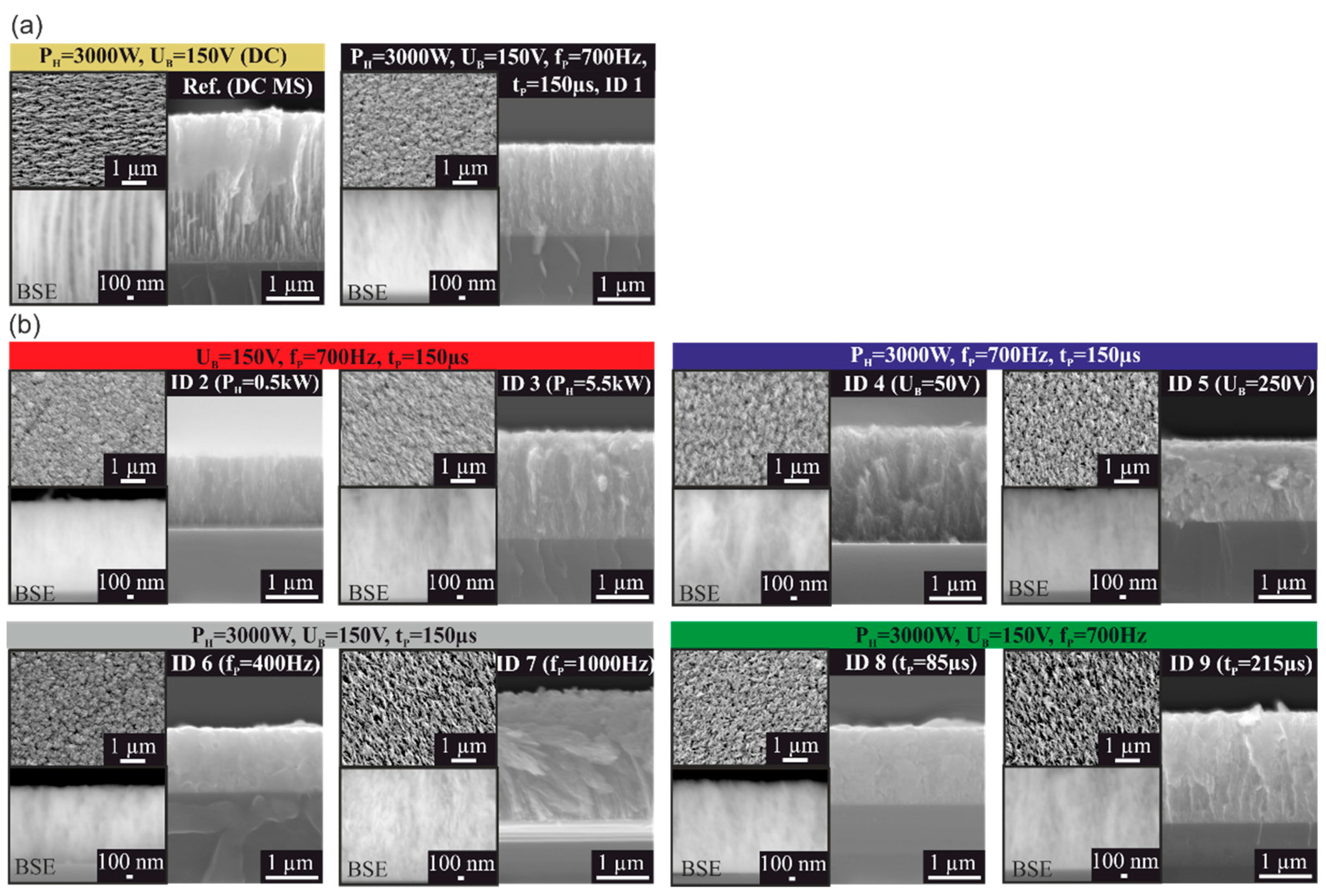
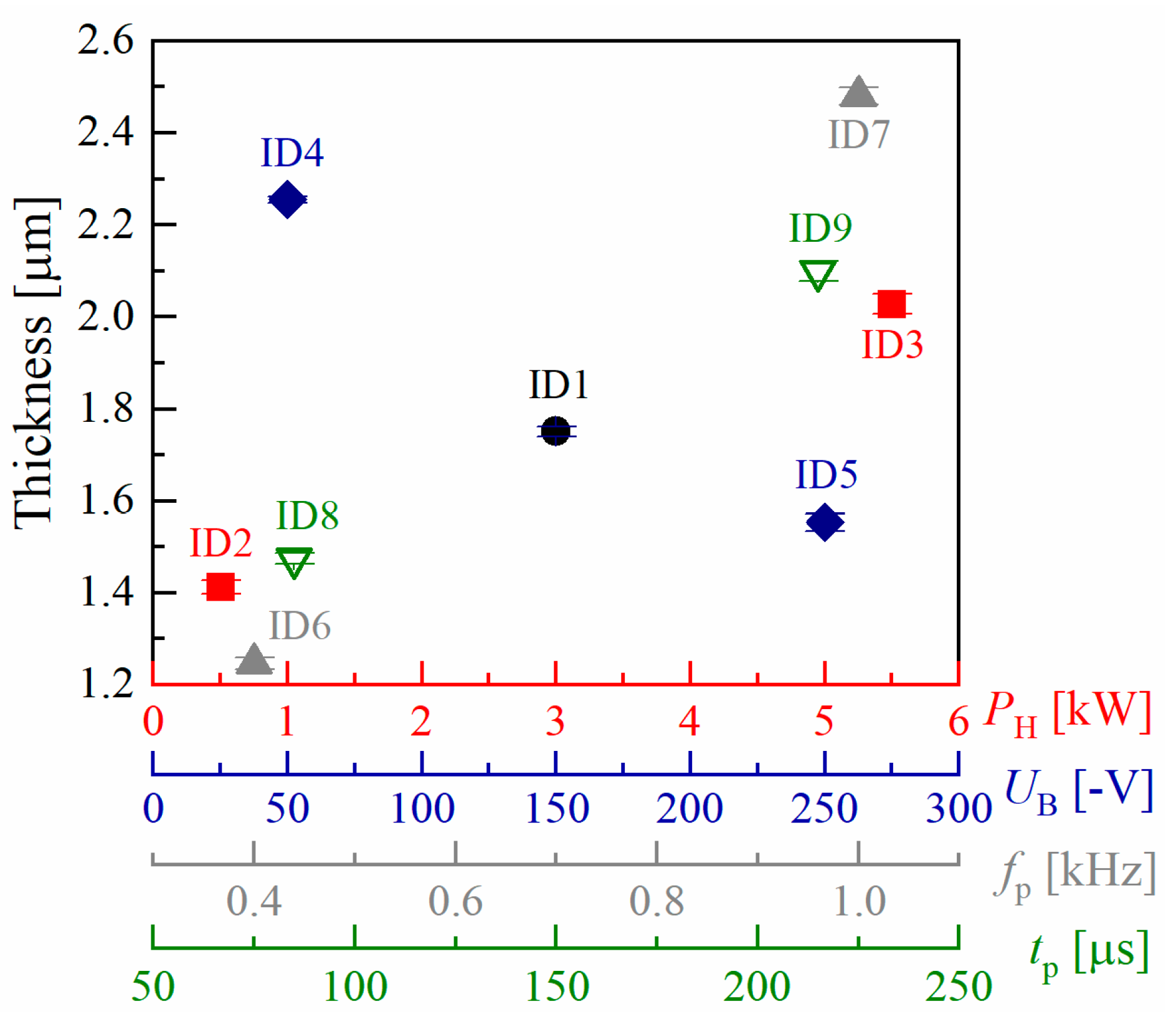
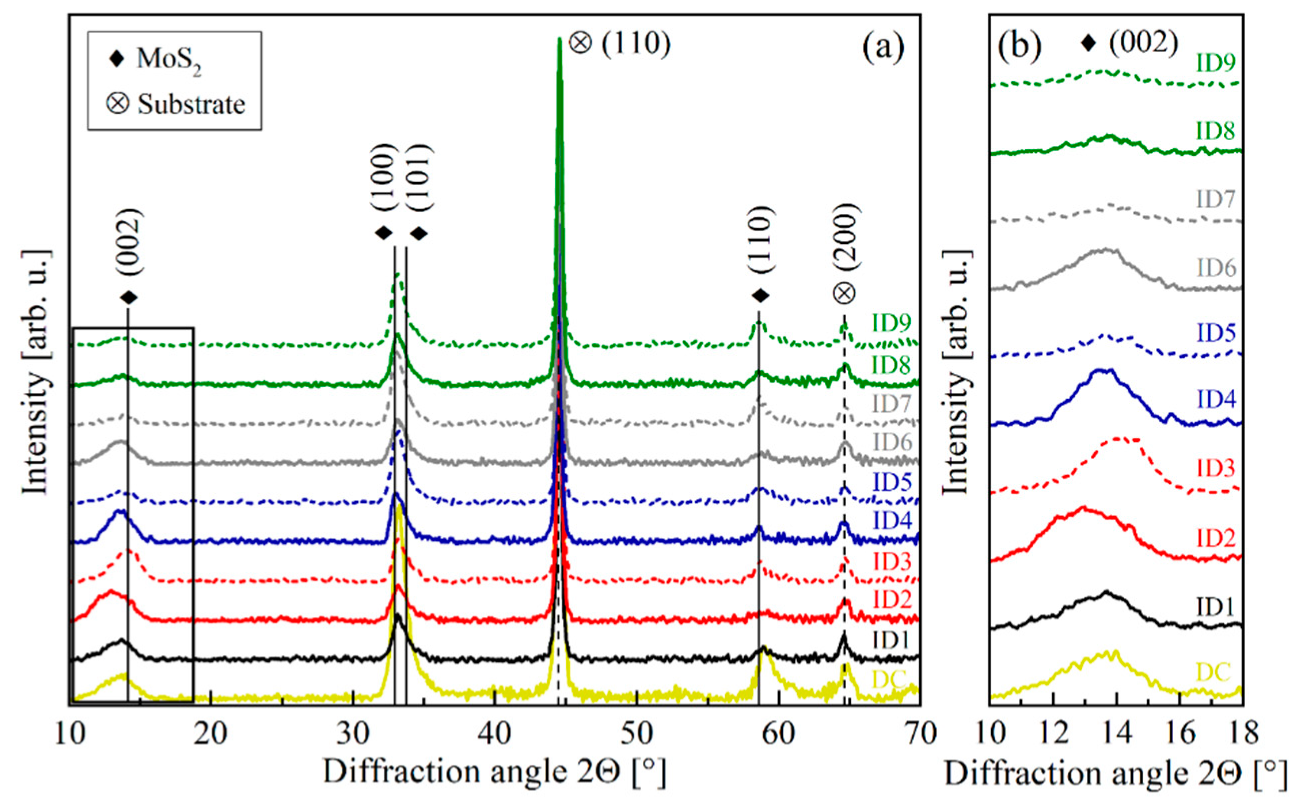
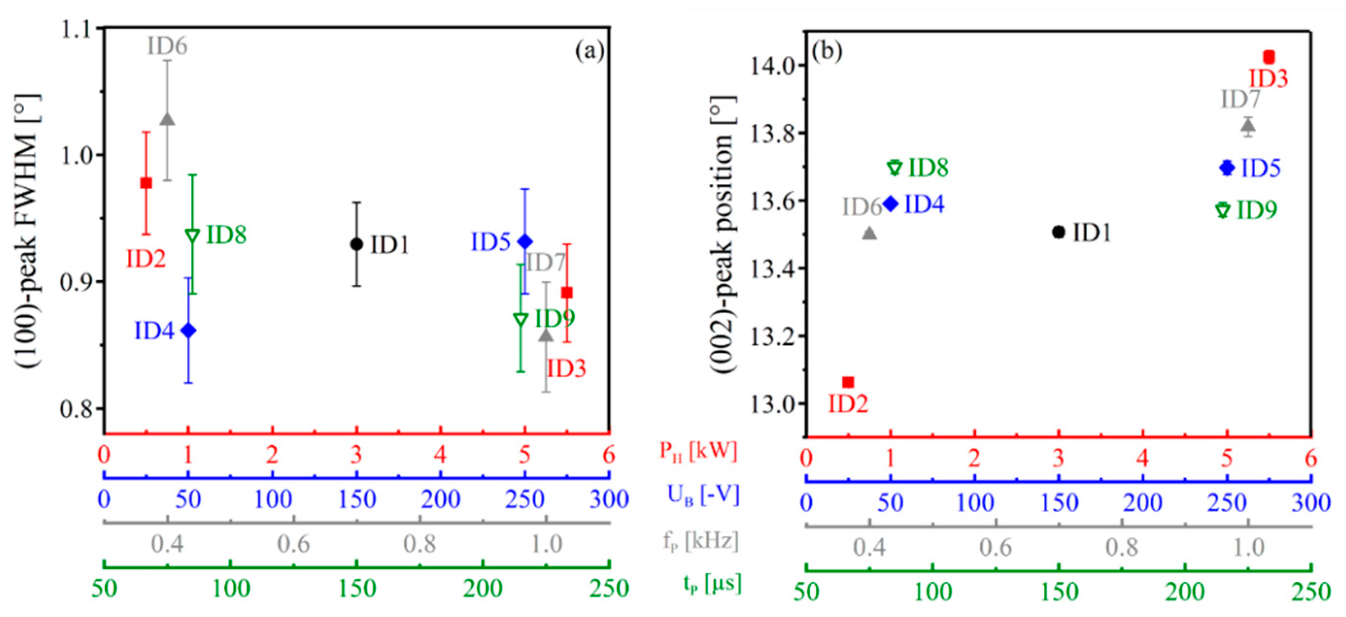
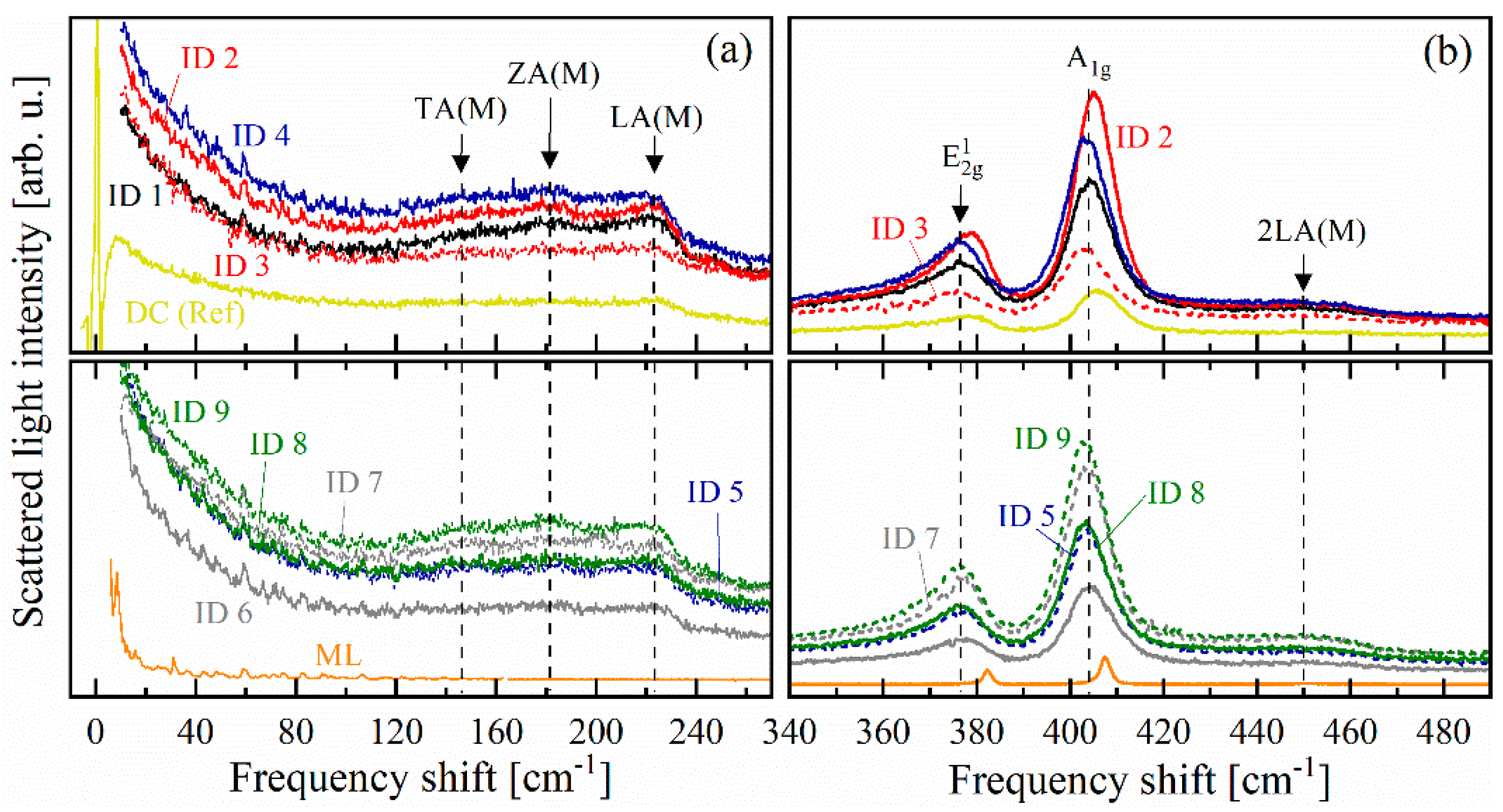
3.1. Structural Properties of the MoSx Films

The surface topographies and cross-section morphologies of the MoSx films grown under different HiPIMS deposition parameters are displayed in Figure 2 (top left and right). The thin films demonstrate a fine and dense morphology which in turn indicates a reduced porosity, which is also evaluated from the images of Figure 2. Nevertheless, most of the films reveal a dendritic needle-like structure. A coarse topography, however, characterizes the reference DC sputtered MoSx film which is comparable to the structure of an RF sputtered MoS2 film [23].
Further insight into the morphology of the films is provided by high magnified SEM images taken in the backscattered-electron (BSE) mode shown at the bottom left of Figure 2. The growth structure of the films ID8, ID5 and ID2 is more homogeneous than that of the other MoSx coatings. Hence, we propose that the homogeneity of the HiPIMS film growth becomes pronounced for a short pulse duration, a high bias-voltage, and a low heating power.
The structural quality of the MoSx film is further elaborated by considering the arithmetic mean roughness Ra. According to Table 1, Ra varies between (12.7 ± 0.5) (ID6) and (80.3 ± 3.7) nm (ID9), for the films grown by the HiPIMS method. The roughness of the reference DC sample amounts to (79.1 ± 1.5) nm and is comparable to that of ID9. The different deposition parameters do not affect the roughness value significantly according to the statistical evaluation presented in Table 2 (p-values above 0.05). Nevertheless, it is observed that the roughness increases with increasing pulse duration from (16.9 ± 3.3) nm (tp = 85 µs), to (18.6 ± 0.7) nm (tp = 150 µs) to (80.3 ± 3.7) nm (tp = 215 µs), for ID8, ID1 and ID9, respectively. The aforementioned trend to obtain a low surface roughness with temporally narrow pulses corresponds with the SEM data on the morphology and topography of homogeneous MoSx films. Accordingly, the ID8 sample with a smooth surface (Ra ~ 17 nm) grown at tp = 85 µs has a more homogeneous structure than the MoSx coatings deposited at higher pulse durations.
The cross-section SEM images moreover indicate that the deposition parameters affect the coating thickness d in different ways. These dependences are depicted in Figure 3. A high thickness, deduced from the cross-sectional images, of the MoSx coatings is achieved with increasing heating power, pulse duration and frequency. This trend is also indicated by the positive t-values in Table 2. Increasing the absolute value of the negative bias-voltage (t-value < 0) leads to a narrowing of the MoSx film. For instance, the lowest thickness d = (1.25 ± 0.01) µm and the highest one d = (2.48 ± 0.02) µm are obtained for the ID6 and ID7, respectively. The thickness of the reference coating amounts to (2.70 ± 0.02) µm, see Table 1. According to the statistical evaluation, see Table 2, the pulse frequency and bias-voltage exhibit the highest impact on the coating thickness. Furthermore, the substrate temperature TS defined by the heating power is important for controlling the coating thickness; considering the samples ID2 and ID3, a high substrate temperature is related to a large coating thickness.
The film-thickness dependence is additionally studied by the impact of the peak current density on the deposition rate. Papa et al. [43] ascribed a lowering of the deposition rate and coating thickness to an increased peak current density. For Cr sputtering, an increase in the deposition rate is observed with rising peak current density only up to a threshold value of about 570 mA/cm2 [44]. For higher densities, the deposition rate decreases owing to self-sputtering effects. To calculate the maximum peak current density, the oscilloscope data were taken and the measured maximum current of the individual pulses associated with the target size of (500 × 88) mm². Taking into account exemplarily the films ID5 (fp = 700 Hz, UB = −250 V) and ID7 (fp = 1000 Hz, UB = −150 V), the maximum peak current density is (658 ± 9) mA/cm2 (ID5) and (543 ± 7) mA/cm2 (ID7). Indeed, the coating ID5 is about 0.9 µm thinner than that of ID7. A narrowing of the MoSx film thickness may be caused not only by a self or resputtering for peak current densities above a threshold value, but also by a densification of the film resulting from a high bias-voltage. The latter aspect has been shown within the analysis of the SEM images and was observed in MoSx [37] and MoS2-Ti films [19].
The ratio between the Mo and S atoms within the MoSx films was evaluated from EDS measurements of the chemical composition. As listed in Table 1, the HiPIMS grown MoSx films exhibit S/Mo ratios between 2.02 ± 0.02 (ID1) and 2.22 ± 0.05 (ID2), which are higher than that of an MoS2 alloy. Accordingly, the sulfur content of all HiPIMS grown films is higher than 66.6 at.%. A lower ratio of 1.59 ± 0.02 is measured for the DC sputtered film. The change from the DC to the HiPIMS growth method demonstrates the highest influence on the stoichiometry of the MoSx films from 1.59 to 2.13 on average, although both methods used the same average cathode power. This leads to the conclusion that the ionization of the sputtered material by using different power supplies plays a superordinate role. Among the HiPIMS films the increase in the substrate temperature, caused by an enhanced heating power, seems to reduce the S/Mo ratio towards 2. By increasing the substrate temperature from 100 to 300 °C a decrease of the S/Mo ratio from 1.90 to 1.71 is reported for DC sputtered thin films [15]. S/Mo ratios between 0.8 and 1.5 are obtained for bipolar pulsed magnetron sputtered MoSx thin films [45]. According to reference [16], an increasing bias-voltage results in a reduction of the S/Mo ratio due to resputtering and an enhanced ion bombardment. These effects are most likely to be found in the resputtering of sulfur since it has a lower atomic mass than molybdenum. Therefore, we attribute an appearance of selective resputtering of sulfur atoms to the DC sputtered reference sample. The constant resputtering in case of the direct-current-bias leads to a higher selective resputtering due to the higher duty cycle compared to the synchronized-pulsed bias of the HiPIMS processes.
The XRD spectra of the MoSx films are shown in Figure 4a,b. Several peaks are observed in the analyzed 2 θ -range. The diffraction peaks at about 44° and 64° stem from the 100Cr6 substrate, while the other Bragg peaks are attributed to diffractions from the (002), (100), (101) and (110) planes of MoSx. The presence of such a number of peaks indicates that the films reveal a polycrystalline structure [46]. Moreover, for MoSx coatings with x > 1.3, the formation of a hexagonal atomic arrangement has the highest probability [18]. A regular atomic arrangement manifests itself in narrow peak linewidths. The diffraction peaks of the MoSx films are quite broad. The broadening results from either an increase in the residual strain, leading to an imperfect crystalline ordering within the films, or a size narrowing of crystallites formed at the surface [47]. The latter aspect is governed by the Scherrer equation D = K λ / ( β cos θ ) which relates the average crystallite size D with the diffraction angle θ , the excitation wavelength λ , the shape factor K = 0.89 and the full width at half maximum (FWHM) denoted by β [48]. For the (100) peak, the mean crystallite size is given by (9.4 ± 1.0) nm.
Due to broadening, the (100) and (101) diffraction peaks of MoSx overlap with each other at about 2Θ = 33.2°, for most films. The FWHM of the intense (100) peak is shown in Figure 5a as function of the deposition parameters. A considerable decrease in the FWHM is observed with increasing the pulse frequency; the p-value is given by 0.0092 (see Table 2). For instance, the FWHM of the (100) peak of ID6 (400 Hz) amounts to 1.03° ± 0.05°, while it is 0.86° ± 0.04° for ID7 (1000 Hz). An enhanced pulse frequency in a HiPIMS film synthetization is connected to the transfer of a large number of atoms with high kinetic energies to the sample. During the nucleation process of these mobile atoms they lose energy in a specific time. Changing the pulse frequency alters the dynamics including atomic collisions and the energy dissipation of the atoms at the surface. For a high pulse frequency, a large number, i.e., a sea of high-kinetic Mo and S atoms is present at the surface. In this collective state the atoms take such lattice positions that the surface energy is minimized [49]. As a result, the atoms form a quite crystalline lattice which is indicated by a small XRD-peak FWHM. In turn, the increase in the substrate temperature gives rise to a narrowing of the (100) peak. Moreover, the high kinetic energy and mobility of the Mo and S atoms at the surface may result in a reduced internal strain and, respectively, in the formation of large-sized crystallites. In particular, the former aspect agrees with the observation that, for a high substrate temperature, the stoichiometry ratio of x = 2 for MoSx is realized. This is assigned to a high surface diffusion during the growth process, and to a relaxation of strain within the MoS2 film.
By comparison, the (002) peak shows a wide broadening in most of the MoSx films, see Figure 5b. For an increasing bias-voltage, for example, the diffraction peak changes from a symmetric, pronounced profile (ID4) to a weak (ID1) and negligible (ID5) shape. The (002) peak indicates the presence of a well-stacked layered structure along the (002) crystal direction [50]. The shift in the position of the (002) peak (see Figure 5b) is attributed to a change in the distance between the atomic layers along the (002) stacking. Since the Bragg diffraction angle is inversely proportional to the distance, the distance between the stacked layers is enlarged for ID2 (2Θ = 13.07° ± 0.01°) and ID4, while it becomes smaller, in particular for ID3 (2Θ = 14.04° ± 0.02°). An increase in the heating power, as indicated by a large positive t-value for the substrate temperature in Table 2, causes a shift of the (002) peak to large diffraction angles: the spacing between the layers along the (002) direction becomes smaller. Since a high heating power or high substrate temperature significantly drives the S/Mo ratio towards 2, fewer sulfur atoms are arranged within the layers so that the interlayer spacing is reduced.
Considering the intensities of the (002) and (100) peaks, we see that the (100)/(002) intensity ratio differs strongly among the MoSx films. For the samples ID9, ID7 and ID5 the ratio is large, see Table 1; thus, these films are predominantly (100)-oriented. The XRD patterns of the other films are contributed by the (101) peak and a broad (002) peak which furthermore shifts in its position. Interestingly, neither the surface roughness nor the coating thickness can be correlated to the preferential film orientation along the (100) direction.
The inelastic light-scattering spectra of the different MoSx HiPIMS coatings and of a mechanically exfoliated MoS2 monolayer are shown in Figure 6. In panel (a) the disorder-induced acoustic-phonon lines at about 150, 180 and 230 cm−1 are depicted [51], while in panel (b) the E 2 g 1 Raman mode at about 376 cm1, the A 1 g mode at about 405 cm−1, and the weak 2LA(M) mode at about 450 cm−1 are observed [52].
In comparison to the mean spectral positions of the A 1 g and E 2 g 1 modes indicated by the vertical dashed lines in Figure 6b, the modes shift to lower frequencies for ID3 and, in particular, to higher frequencies for ID2. The main difference between these HiPIMS films is the different heating powers used. The low- (high-)frequency shift occurs for the MoSx film grown by a high (low) heating power. In turn, this correlation can be transferred to the substrate temperature. The E 2 g 1 ( A 1 g ) phonon mode describes an in-plane (out-of-plane) vibration of Mo and S atoms [53]. The scattering frequency is generally connected via Δ E W / ( l m ) to the bonding length l and the interaction strength W between the atoms with effective mass m. Based on the frequency shifts, we assume that with increasing heating power or, respectively, substrate temperature, the bonding become longer and, in turn, the coupling strength decreases. It is in agreement with the behavior that at a high temperature and, respectively, large thermal energy, the lattice becomes relaxed. The relaxation results in a bond length adjustment/adaption with respect to the equilibrium (electrostatic) atomic positions. Since these lattice vibrations are not connected to the interlayer spacings, the inelastic light scattering results shall not be brought into relation to the XRD results concerning the (002) diffraction peak.
The linewidths of the optical phonon modes at about 390 cm−1 and the acoustic phonons at about 180 cm−1 are broad for all films studied. They are broader than the typically observed lines in MoS2 layered structures or bulk crystals [36,54] and in HiPIMS MoSx films [36,54]. On the one hand, the broadening may be assigned to a non-uniform stoichiometric ratio of the Mo and S atoms. The variation in the coordination and termination of the bonding thus increases the dispersion of the scattering frequencies. On the other hand, the line broadening may be related to the degree of non-single crystallinity of the MoSx coatings. Accordingly, the bonds between the Mo and S atoms have different lengths and coupling strengths.
For ID1, ID2 and ID9 (see Figure 6a) the acoustic phonon modes are quite pronounced. They were grown at the low and central heating power or, respectively, at large pulse duration. We assume that the slight sharpening of the acoustic phonon modes indicates a reduced inhomogeneity in the structural composition of the HiPIMS coatings. The lattice could be arranged in a slightly more uniform way and the spatial distribution of the crystallite sizes may be more homogeneous. This assumption would agree with the aforementioned characterization results for the respective MoSx films.
In comparison to the scattering spectrum of the MoS2 monolayer (see the orange curve in Figure 6) the optical phonon modes are shifted—to low frequencies on the whole. Actually, for micrometer-thin MoS2 layers, the E 2 g   1 ( A 1 g ) Raman line shifts to lower (higher) frequencies, so that the spectral distance between the peaks enlarges [54]. Here, both Raman lines shift however to low frequencies. This behavior is probably due to the adsorption of nitrogen since a surface coverage of about 10% nitrogen yields a shift of about −7 cm1 of both lines [55].

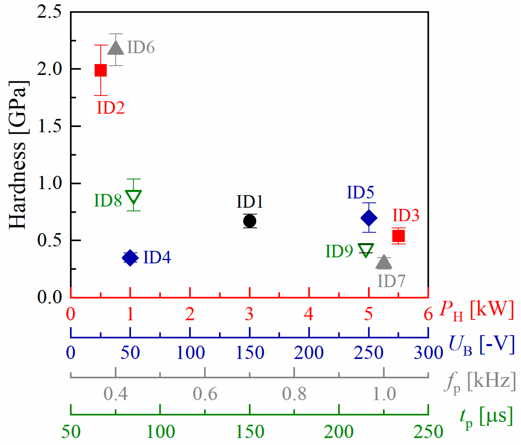
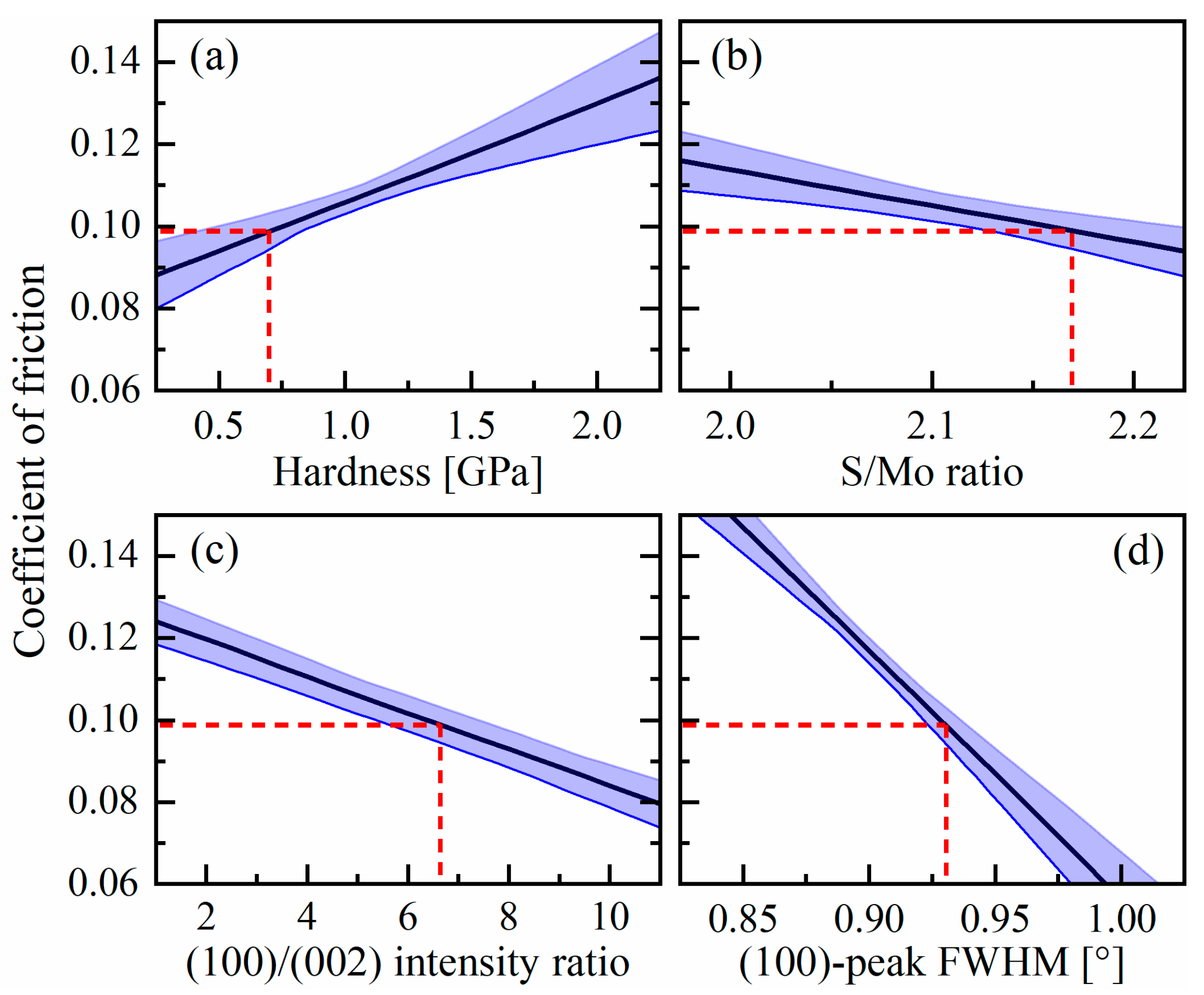
3.2. Mechanical and Tribological Properties

The hardness and Young’s modulus are also studied in dependence on the HiPIMS deposition parameters. In Figure 7 the hardness of the different MoSx films are shown as functions of the heating power, bias-voltage, pulse frequency and duration. Since Young’s modulus behaves similarly, it is not graphically demonstrated. Table 3 lists the hardness H and elastic modulus E values as well as their ratios, which only slightly differ from each other. A clear dependence of the hardness on the heating power and pulse frequency is indicated in Figure 7. The hardness of the MoSx films is enhanced from less than 0.5 to 2 GPa by lowering the heating power/substrate temperature and pulse frequency. In detail, the hardness of the films varies between (0.3 ± 0.1) GPa, for ID7, and (2.2 ± 0.1) GPa, for ID6. The Young’s modulus varies between (31.5 ± 4.2) GPa for ID7, and (90.3 ± 8.6) GPa for ID6. Accordingly, the H/E ratio of the coatings ranges between 0.010 and 0.025. For direct-current unbalanced magnetron sputtered MoS2 thin films, an increase in the hardness was related to a low substrate temperature [56], and hardness (Young’s modulus) values between 0.2 (15.6 GPa) [23] and 2.0 GPa (51.1 GPa) [56] were reported.
The elastic modulus and, in turn, the hardness of a polar covalent material depends merely on the ionicity and bonding length [57]. MoS2 is a polar covalent material, since the difference between the electronegativities of Mo with XMo = 2.16 and S with XS = 2.58 exceeds 0.4, for a single bonding. The ionicity I is proportional to 1 exp [ ( X A X B ) 2 4 ] ; for the hardness, the relation H exp ( 1.2   I ) / l 2.5 was evaluated [57]. A small ionicity, given for a small electronegativity difference, leads to a large hardness value assuming that the bonding length l remains constant. This is in agreement with the fact that covalent bonds typically have a higher hardness than ionic bonds [58]. For the MoSx films, the stoichiometry ratio S/Mo is often larger than 2. Thus, the larger number of sulfur atoms polarize the Mo-S bonding more strongly, endowing the molybdenum atoms with more positive charge than the sulfur atoms, and both the electronegativity difference as well as I increase. As a result, most of the MoSx films studied exhibit small hardness values. Only the thin films ID2 and ID6 deviate from this observation. The ID2 film was grown at a low substrate temperature and, on basis of the Raman scattering results, the Mo-S bonding length l is short. Since the hardness scales with l 2.5 , the distance shortening between the Mo and S atoms plays an important role for this coating. For ID6, the presence of small crystallites has been deduced from the XRD data. Small crystallites with sizes in the 10 nm range lead to a high elastic stiffness and hardness in accordance with the Hall–Petch strengthening [59].
The friction coefficients of the thin films were obtained by ball-on-disc experiments in order to analyze the influence of the HiPIMS deposition parameters on the suitability of the MoSx coatings for tribological applications. The friction coefficients of the reference DC and HiPIMS MoSx films are listed in Table 3. The friction coefficients of the different films do not differ significantly from each other using the uncoated or MoSx-coated 100Cr6 counter body. The friction coefficient μ differs from 0.10 ± 0.02 (ID5) to 0.16 ± 0.03 (ID4) using the uncoated counter body, while μ changes between 0.09 ± 0.01 (ID5) and 0.16 ± 0.05 (ID3), for the coated counter body. The lowest friction coefficient is shown by ID5. In comparison to that, for the DC sputtered reference film the friction coefficients amount to only 0.05 ± 0.1 against 100Cr6 and 0.10 ± 0.03 against MoSx. For magnetron sputtered MoS2 films, friction coefficients ranging between 0.11 and 0.22 are typically reported [22,56]. The friction coefficient is strongly influenced by the chemical composition and hardness of the coatings [18]. According to Aubert et al. the minimum friction coefficient could be obtained for S/Mo ratios between 1.5 and 1.6 [18]. The low friction coefficient may be ascribed to the basal (002) orientation within the MoSx film [20,36].
Taking exemplarily film ID5 into account, linear correlations between the coefficient of friction and the most significant structural properties are calculated and displayed in Figure 8. The properties are given by the (100)/(002) XRD-peak intensity ratio (p = 0.0001, t = −17.26), the XRD-(100)-peak FWHM (p = 0.0001, t = −15.48), the hardness (p = 0.0025, t = −6.74) and the S/Mo ratio (p = 0.0057, t = −5.41). An increase in the (100)/(002) intensity ratio, the (100)-peak FWHM and the S/Mo ratio, and a decrease in the hardness is related to a reduction in the friction coefficient. These linear correlations indicate that the friction coefficient depends on several structural and mechanical properties of the MoSx film. Moreover, the dependences on the FWHM and S/Mo ratio agree with the experimentally obtained data that, for a high substrate temperature and/or pulse frequency, an XRD line narrowing and a shift of the S/Mo ratio towards 2 are achieved. It is attributed to decreasing the degree of inhomogeneity within the MoSx material. Accordingly, for a more homogeneous structure, the resistance against, for instance, shear forces is enhanced so that the coefficient of friction rises.
The correlation μ ( 100 ) / ( 200 ) (see Figure 8c) shows that a higher intensity of the (002) XRD peak compared to that of the (100) peak, corresponding to a lower (100)/(002) intensity ratio, causes an increase in the friction coefficient. This is contrary to published studies. Generally, a small friction coefficient is observed for magnetron sputtered films showing a basal (002) orientation [36,60]. Didziulis et al. [61] worked out that only the initial friction coefficient depends on the film orientation, since the basal orientation is formed during the tribological contacts and can lead to even lower friction values than a film with initial basal (002) orientation. Concerning the HiPIMS films, a low averaged friction coefficient is achieved for films with a high initial (100) orientation. Accordingly, it seems that, also, the dense microstructure of the HiPIMS films allows tribologically stressed surface areas to change their orientation along the basal (002) direction, as shown in a previous study [37]. Furthermore, an initial (100)-orientation may enhance this process.

4. Conclusions

In summary, the coatings grown by the HiPIMS method demonstrate a fine and dense topography in comparison to the DC sputtered MoSx film. For a high bias-voltage and low heating power, a reduction in the structural inhomogeneity is observed. A high bias-voltage further causes a narrowing of the MoSx film thickness probably due to a resputtering process. A weak heating power leads to a shortening of the Mo-S bonding lengths and an enhancement in the interatomic coupling, for in-plane and out-of-plane lattice vibrations. Increasing the heating power shifts the stoichiometric S/Mo ratio towards 2 which may be attributed to a high surface diffusion during the growth process. A high substrate temperature also gives rise to a reduction in the interlayer spacing along the (002) direction of the polycrystalline MoSx films. The broadening of the phonon modes in the scattered light spectra underlines the non-uniform stoichiometric ratio of the Mo and S atoms and the polycrystalline character of the HiPIMS coatings, which is also demonstrated by the XRD measurements. The XRD data additionally reveal that a high pulse frequency and substrate temperature are related to a diffraction line narrowing. From the microscopic point of view, changing the pulse frequency alters the dynamics including atomic collisions and the energy dissipation of the atoms at the surface. A large number of high-kinetic Mo and S atoms are present at the surface, and the atoms take such lattice positions that the surface energy is minimized. In this collective state a self-organized growth process occurs, like for nanocomposite films [62], so that large crystallites are formed at the surface thus reducing the internal strain. For large pulse frequencies, thick MoSx films are grown which are characterized by a reduced densification. Temporally narrow pulses create smooth surfaces of the MoSx coatings with mean roughness values of less than 15 nm. In comparison to that, the DC sputtered reference sample demonstrates a coarse structure and large thickness.
With respect to the mechanical and tribological properties, it is shown that the hardness of the MoSx films is enhanced from about 0.5 to 2 GPa by lowering the heating power/substrate temperature and pulse frequency. For the films with the highest hardness values it is proposed that the Mo-S bonding length is short and that small-sized crystallites at the surface lead to a high elastic stiffness. The friction coefficients of the HiPIMS films ranging from 0.10 to 0.16 are not significantly affected by the deposition parameters. However, an impact is deduced from specific coating properties, i.e., the (100/002)-XRD-peak intensity ratio, (100)-XRD-peak linewidth, hardness and S/Mo ratio. It is proposed that, for a more homogeneous structure, the resistance against shear forces is enhanced so that the coefficient of the friction is increased. A low averaged friction coefficient is achieved for films with an initial (100) orientation. Therefore, the dense microstructure of the HiPIMS films allows tribologically stressed surface areas to change their orientation along the basal (002) direction, and an initial (100)-orientation may enhance this process.

Author Contributions

Conceptualization, D.K.; validation, D.S.; investigation, D.K., H.M. and A.W.; writing—original draft preparation, D.K., J.D. and A.N.; writing—review and editing, D.S., A.B. and W.T.; supervision, A.B. and W.T.; funding acquisition, W.T., A.B. and J.D. All authors have read and agreed to the published version of the manuscript.

Funding

This research was funded by the Deutsche Forschungsgemeinschaft (German Research Foundation, DFG) within the priority program SPP2074 (Project “Fluid-free lubricant layers for the heavily loaded operation of dry-running twin-screw machines without timing gears”).

Acknowledgments

We acknowledge financial support by Deutsche Forschungsgemeinschaft and Technische Universität Dortmund/TU Dortmund University within the funding programme Open Access Publishing. The authors gratefully acknowledge Dirk Biermann and Eugen Krebs from the Institute of Machining Technology, TU Dortmund University, for confocal 3D microscopy measurements.

Conflicts of Interest

The authors declare no conflict of interest.

References

  1. Brecher, C.; Spachtholz, G.; Bobzin, K.; Lugscheider, E.; Knotek, O.; Maes, M. Superelastic (Cr,Al)N coatings for high end spindle bearings. Surf. Coat. Tech. 2005, 200, 1738–1744. [Google Scholar] [CrossRef]
  2. Mattox, D.M. Handbook of Physical Vapor Deposition (PVD) Processing, 2nd ed.; William Andrew: Oxford, UK, 2010; ISBN 9780815520375. [Google Scholar]
  3. Janicki, M.; Temming, J.; Kauder, K.; Brümmer, A. Simulationsgestützte Entwicklung eines unsynchronisierten Schraubenladers. In (Hrsg.): Motorprozesssimulation und Aufladung II. Haus der Technik Fachbuch Band 83; Pucher, H., Kahrstedt, J., Eds.; Expert-Verlag: Tübingen, Germany, 2007; pp. 146–168. [Google Scholar]
  4. Nikolov, A.; Nadler, K.; Brümmer, A. Experimental and theoretical investigation of screw machines as vacuum blowers. In Proceedings of the 7th International Conference on Compressors and their Systems 2011, City University London, UK, 5–6 September 2011; Elsevier Science: Oxford, UK, 2011; pp. 359–374, ISBN 0857095358. [Google Scholar]
  5. Nikolov, A.; Brümmer, A. Investigating a Small Oil-Flooded Twin-Screw Expander for Waste-Heat Utilisation in Organic Rankine Cycle Systems. Energies 2017, 10, 869. [Google Scholar] [CrossRef] [Green Version]
  6. Moldenhauer, H.; Bayer, M.; Debus, J.; Nikolov, A.; Brümmer, A. Raman scattering study of micrometer-sized spots of magnetite and hematite formed at 18CrNiMo7-6 screw rotor surfaces due to liquid-free, unsynchronized operation. IOP Conf. Ser. Mater. Sci. Eng. 2018, 425, 12016. [Google Scholar] [CrossRef]
  7. Grieb, M.; Brümmer, A. Design and examination of a small-scale screw expander for waste heat recovery. In Proceedings of the International Conference on Screw Machines 2014, TU Dortmund University, Germany, 23–24 September 2014; VDI-Verl.: Düsseldorf, Germany, 2014; pp. 197–210, ISBN 978-3-18-092228-7. [Google Scholar]
  8. Holmberg, K.; Matthews, A. Coatings Tribology. Properties, Mechanisms, Techniques and Applications in Surface Engineering; Elsevier Professional: Oxford, UK, 2009; ISBN 978-0-444-52750-9. [Google Scholar]
  9. Wong, K.C.; Lu, X.; Cotter, J.; Eadie, D.T.; Wong, P.C.; Mitchell, K.A.R. Surface and friction characterization of MoS2 and WS2 third body thin films under simulated wheel/rail rolling–sliding contact. Wear 2008, 264, 526–534. [Google Scholar] [CrossRef]
  10. Wang, Z.M. MoS2: Materials, Physics, and Devices; Lecture Notes in Nanoscale Science and Technology; Springer: Cham, Switzerland, 2014; Volume 21, ISBN 9783319028507. [Google Scholar]
  11. Davim, J.P. Tribology of Nanocomposites; Springer: Berlin/Heidelberg, Germany, 2013; ISBN 9783642338816. [Google Scholar]
  12. Charoo, M.S.; Wani, M.F.; Hanief, M.; Rather, M.A. Tribological Properties of MoS2 Particles as Lubricant Additive on EN31 Alloy Steel and AISI 52100 Steel Ball. Mater. Today Proc. 2017, 4, 9967–9971. [Google Scholar] [CrossRef]
  13. Roberts, E.W. Ultralow friction films of MoS2 for space applications. Thin Solid Films 1989, 181, 461–473. [Google Scholar] [CrossRef]
  14. Nabot, J.-P.; Aubert, A.; Gillet, R.; Renaux, P. Cathodic sputtering for preparation of lubrication films. Surf. Coat. Technol. 1990, 43–44, 629–639. [Google Scholar] [CrossRef]
  15. Fleischauer, P.D.; Hilton, M.R.; Bauer, R. Effects of microstructure and adhesion on performance of sputter-deposited MoS2 solid lubricant coatings. Mech. Coat. Tribol. Ser. 1990, 17, 121–128. [Google Scholar] [CrossRef]
  16. Tillmann, W.; Wittig, A.; Stangier, D.; Thomann, C.-A.; Moldenhauer, H.; Debus, J.; Aurich, D.; Brümmer, A. Investigation of the Tribofilm Formation of HiPIMS Sputtered MoSx Thin Films in Different Environments by Raman Scattering. Lubricants 2019, 7, 100. [Google Scholar] [CrossRef] [Green Version]
  17. Li, Y.; Xie, M.; Sun, Q.; Xu, X.; Fan, X.; Zhang, G.; Li, H.; Zhu, M. The effect of atmosphere on the tribological behavior of magnetron sputtered MoS2 coatings. Surf. Coat. Technol. 2019, 378, 125081. [Google Scholar] [CrossRef]
  18. Aubert, A.; Nabot, J.P.; Ernoult, J.; Renaux, P. Preparation and properties of MoSx films grown by d.c. magnetron sputtering. Surf. Coat. Technol. 1990, 41, 127–134. [Google Scholar] [CrossRef]
  19. Bülbül, F.; Efeoğlu, İ. Synergistic effect of bias and target currents for magnetron sputtered MoS2 -Ti composite films. Mater. Test. 2016, 58, 471–474. [Google Scholar] [CrossRef]
  20. Vierneusel, B.; Tremmel, S.; Wartzack, S. Effects of deposition parameters on hardness and lubrication properties of thin MoS 2 films. Materialwiss. Werkst. 2012, 43, 1029–1035. [Google Scholar] [CrossRef]
  21. Bellido-González, V.; Jones, A.H.S.; Hampshire, J.; Allen, T.J.; Witts, J.; Teer, D.G.; Ma, K.J.; Upton, D. Tribological behaviour of high performance MoS2 coatings produced by magnetron sputtering. Surf. Coat. Technol. 1997, 97, 687–693. [Google Scholar] [CrossRef]
  22. Serpini, E.; Rota, A.; Ballestrazzi, A.; Marchetto, D.; Gualtieri, E.; Valeri, S. The role of humidity and oxygen on MoS2 thin films deposited by RF PVD magnetron sputtering. Surf. Coat. Technol. 2017, 319, 345–352. [Google Scholar] [CrossRef]
  23. Zhang, X.; Qiao, L.; Chai, L.; Xu, J.; Shi, L.; Wang, P. Structural, mechanical and tribological properties of Mo–S–N solid lubricant films. Surf. Coat. Technol. 2016, 296, 185–191. [Google Scholar] [CrossRef]
  24. Hilton, M.R.; Bauer, R.; Didziulis, S.V.; Dugger, M.T.; Keem, J.M.; Scholhamer, J. Structural and tribological studies of MoS2 solid lubricant films having tailored metal-multilayer nanostructures. Surf. Coat. Technol. 1992, 53, 13–23. [Google Scholar] [CrossRef]
  25. Roberts, E.W.; Williams, B.J.; Ogilvy, J.A. The effect of substrate surface roughness on the friction and wear of sputtered MoS2 films. J. Phys. D Appl. Phys. 1992, 25, A65–A70. [Google Scholar] [CrossRef]
  26. Wong, W.C.; Ng, S.M.; Wong, H.F.; Cheng, W.F.; Mak, C.L.; Leung, C.W. Effect of post-annealing on sputtered MoS2 films. Solid State Electron. 2017, 138, 62–65. [Google Scholar] [CrossRef]
  27. Gilmore, R.; Baker, M.A.; Gibson, P.N.; Gissler, W.; Stoiber, M.; Losbichler, P.; Mitterer, C. Low-friction TiN–MoS2 coatings produced by dc magnetron co-deposition. Surf. Coat. Technol. 1998, 108-109, 345–351. [Google Scholar] [CrossRef]
  28. Amaro, R.I.; Martins, R.C.; Seabra, J.O.; Renevier, N.M.; Teer, D.G. Molybdenum disulphide/titanium low friction coating for gears application. Tribol. Int. 2005, 38, 423–434. [Google Scholar] [CrossRef]
  29. Sun, L.; Ruan, T.; Yuan, Z.; Fang, Q.; Gong, W.; Wu, X.; Mei, S. Microstructures and properties of Mo2N+MoS2 coatings deposited by direct current magnetron sputtering. Vacuum 2020, 177, 109406. [Google Scholar] [CrossRef]
  30. Zhang, R.; Cui, Q.; Weng, L.; Sun, J.; Hu, M.; Fu, Y.; Wang, D.; Jiang, D.; Gao, X. Modification of structure and wear resistance of closed-field unbalanced-magnetron sputtered MoS2 film by vacuum-heat-treatment. Surf. Coat. Technol. 2020, 126215. [Google Scholar] [CrossRef]
  31. Ehiasarian, A.P.; Vetushka, A.; Hecimovic, A.; Konstantinidis, S. Ion composition produced by high power impulse magnetron sputtering discharges near the substrate. J. Appl. Phys. 2008, 104, 83305. [Google Scholar] [CrossRef]
  32. Lewin, E.; Loch, D.; Montagne, A.; Ehiasarian, A.P.; Patscheider, J. Comparison of Al–Si–N nanocomposite coatings deposited by HIPIMS and DC magnetron sputtering. Surf. Coat. Technol. 2013, 232, 680–689. [Google Scholar] [CrossRef]
  33. Kamath, G.; Ehiasarian, A.P.; Purandare, Y.; Hovsepian, P.E. Tribological and oxidation behaviour of TiAlCN/VCN nanoscale multilayer coating deposited by the combined HIPIMS/(HIPIMS-UBM) technique. Surf. Coat. Technol. 2011, 205, 2823–2829. [Google Scholar] [CrossRef]
  34. Ehiasarian, A.P.; Münz, W.-D.; Hultman, L.; Helmersson, U.; Petrov, I. High power pulsed magnetron sputtered CrNx films. Surf. Coat. Technol. 2003, 163, 267–272. [Google Scholar] [CrossRef]
  35. Bobzin, K.; Brögelmann, T.; Kruppe, N.C.; Basturk, S.; Klocke, F.; Mattfeld, P.; Trauth, D.; Hild, R. Synthesis, characterization, and tribological evaluation of HPPMS (Cr1−xAlx)N + MoSy coatings. Surf. Coat. Technol. 2016, 308, 383–393. [Google Scholar] [CrossRef]
  36. Moldenhauer, H.; Wittig, A.; Kokalj, D.; Stangier, D.; Brümmer, A.; Tillmann, W.; Debus, J. Resonant Raman scattering characterization of thermally annealed HiPIMS deposited MoS coatings. Surf. Coat. Technol. 2019, 377, 124891. [Google Scholar] [CrossRef]
  37. Tillmann, W.; Wittig, A.; Stangier, D.; Moldenhauer, H.; Thomann, C.-A.; Debus, J.; Aurich, D.; Bruemmer, A. Influence of the bias-voltage, the argon pressure and the heating power on the structure and the tribological properties of HiPIMS sputtered MoSx films. Surf. Coat. Technol. 2020, 385, 125358. [Google Scholar] [CrossRef]
  38. Arslan, E.; Baran, Ö.; Efeoglu, I.; Totik, Y. Evaluation of adhesion and fatigue of MoS2–Nb solid-lubricant films deposited by pulsed-dc magnetron sputtering. Surf. Coat. Technol. 2008, 202, 2344–2348. [Google Scholar] [CrossRef]
  39. Debus, J.; Schindler, J.J.; Waldkirch, P.; Goeke, S.; Brümmer, A.; Biermann, D.; Bayer, M. Indication of worn WC/C surface locations of a dry-running twin-screw rotor by the oxygen incorporation in tungsten-related Raman modes. Appl. Phys. Lett. 2016, 109, 171601. [Google Scholar] [CrossRef]
  40. Siu, K.W.; Ngan, A.H.W. The continuous stiffness measurement technique in nanoindentation intrinsically modifies the strength of the sample. Philos. Mag. 2013, 93, 449–467. [Google Scholar] [CrossRef]
  41. Oliver, W.C.; Pharr, G.M. An improved technique for determining hardness and elastic modulus using load and displacement sensing indentation experiments. J. Mater. Res. 1992, 7, 1564–1583. [Google Scholar] [CrossRef]
  42. Woo, S.; Park, H.C.; Son, Y.-W. Poisson’s ratio in layered two-dimensional crystals. Phys. Rev. B 2016, 93, 543. [Google Scholar] [CrossRef] [Green Version]
  43. Papa, F.; Gerdes, H.; Bandorf, R.; Ehiasarian, A.P.; Kolev, I.; Braeuer, G.; Tietema, R.; Krug, T. Deposition rate characteristics for steady state high power impulse magnetron sputtering (HIPIMS) discharges generated with a modulated pulsed power (MPP) generator. Thin Solid Films 2011, 520, 1559–1563. [Google Scholar] [CrossRef]
  44. Alami, J.; Sarakinos, K.; Mark, G.; Wuttig, M. On the deposition rate in a high power pulsed magnetron sputtering discharge. Appl. Phys. Lett. 2006, 89, 154104. [Google Scholar] [CrossRef] [Green Version]
  45. Lauwerens, W.; Wang, J.; Navratil, J.; Wieërs, E.; D’haen, J.; Stals, L.M.; Celis, J.P.; Bruynseraede, Y. Humidity resistant MoSx films prepared by pulsed magnetron sputtering. Surf. Coat. Technol. 2000, 131, 216–221. [Google Scholar] [CrossRef]
  46. Chromik, S.; Rosová, A.; Dobročka, E.; Kobzev, A.P.; Hulman, M.; Sojkova, M.; Hutár, P.; Machajdík, D. MoS2 thin films prepared by sulfurization. In Proceedings of the Nanoengineering, Fabrication, Properties, Optics, and Devices XIV. Nanoengineering: Fabrication, Properties, Optics, and Devices XIV, San Diego, CA, USA, 6–10 August 2017; SPIE Press: Bellingham, WA, USA, 2017; p. 56, ISBN 9781510611658. [Google Scholar]
  47. Shafi, P.M.; Bose, A.C. Impact of crystalline defects and size on X-ray line broadening: A phenomenological approach for tetragonal SnO2 nanocrystals. AIP Adv. 2015, 5, 57137. [Google Scholar] [CrossRef]
  48. Ingham, B.; Toney, M.F. X-ray diffraction for characterizing metallic films. In Metallic Films for Electronic, Optical and Magnetic Applications: Structure, Processing and Properties; Barmak, K., Coffey, K., Eds.; Woodhead Publishing Limited: Oxford, UK, 2014; pp. 3–38. ISBN 9780857090577. [Google Scholar]
  49. Lüth, H. Solid Surfaces, Interfaces and Thin Films; Springer: Berlin/Heidelberg, Germany, 2010; ISBN 9783642135910. [Google Scholar]
  50. Goloveshkin, A.S.; Bushmarinov, I.S.; Lenenko, N.D.; Buzin, M.I.; Golub, A.S.; Antipin, M.Y. Structural Properties and Phase Transition of Exfoliated-Restacked Molybdenum Disulfide. J. Phys. Chem. C 2013, 117, 8509–8515. [Google Scholar] [CrossRef]
  51. Mignuzzi, S.; Pollard, A.J.; Bonini, N.; Brennan, B.; Gilmore, I.S.; Pimenta, M.A.; Richards, D.; Roy, D. Effect of disorder on Raman scattering of single-layer MoS2. Phys. Rev. B 2015, 91. [Google Scholar] [CrossRef] [Green Version]
  52. Placidi, M.; Dimitrievska, M.; Izquierdo-Roca, V.; Fontané, X.; Castellanos-Gomez, A.; Pérez-Tomás, A.; Mestres, N.; Espindola-Rodriguez, M.; López-Marino, S.; Neuschitzer, M.; et al. Multiwavelength excitation Raman scattering analysis of bulk and two-dimensional MoS2: Vibrational properties of atomically thin MoS2 layers. 2D Mater. 2015, 2, 35006. [Google Scholar] [CrossRef] [Green Version]
  53. Molina-Sánchez, A.; Wirtz, L. Phonons in single-layer and few-layer MoS2 and WS2. Phys. Rev. B 2011, 84, 155413. [Google Scholar] [CrossRef] [Green Version]
  54. Najmaei, S.; Liu, Z.; Ajayan, P.M.; Lou, J. Thermal effects on the characteristic Raman spectrum of molybdenum disulfide (MoS2) of varying thicknesses. Appl. Phys. Lett. 2012, 100, 13106. [Google Scholar] [CrossRef] [Green Version]
  55. Qian, Q.; Zhang, Z.; Chen, K.J. In Situ Resonant Raman Spectroscopy to Monitor the Surface Functionalization of MoS2 and WSe2 for High-k Integration: A First-Principles Study. Langmuir 2018, 34, 2882–2889. [Google Scholar] [CrossRef]
  56. Vierneusel, B.; Schneider, T.; Tremmel, S.; Wartzack, S.; Gradt, T. Humidity resistant MoS2 coatings deposited by unbalanced magnetron sputtering. Surf. Coat. Technol. 2013, 235, 97–107. [Google Scholar] [CrossRef]
  57. Gao, F.M.; Gao, L.H. Microscopic models of hardness. J. Superhard Mater. 2010, 32, 148–166. [Google Scholar] [CrossRef] [Green Version]
  58. Sharma, K.K.; Sharma, L.K. A Textbook of Physical Chemistry. For BSc Students of All Indian Universities Under CBCS, 6th ed.; Vikas Publishing House: Noida, India, 2016; ISBN 9352590422. [Google Scholar]
  59. Zhang, S. Nanostructured Thin Films and Coatings. Mechanical Properties; CRC Press: Hoboken, NJ, USA, 2010; ISBN 9781420094022. [Google Scholar]
  60. Zhang, X.; Vitchev, R.G.; Lauwerens, W.; Stals, L.; He, J.; Celis, J.-P. Effect of crystallographic orientation on fretting wear behaviour of MoSx coatings in dry and humid air. Thin Solid Films 2001, 396, 69–77. [Google Scholar] [CrossRef]
  61. Didziulis, S.V.; Fleischauer, P.D.; Soriano, B.L.; Gardos, M.N. Chemical and tribological studies of MoS2 films on SiC substrates. Surf. Coat. Technol. 1990, 43–44, 652–662. [Google Scholar] [CrossRef]
  62. Lundin, D.; Minea, T.; Gudmundsson, J.T. (Eds.) High Power Impulse Magnetron Sputtering. Fundamentals, Technologies, Challenges and Applications; Elsevier: Amsterdam, The Netherlands, 2020; ISBN 0128124547. [Google Scholar]
Figure 1. (a) Arrangement and target setup in the deposition chamber and (b) experimental setup of the ball-on-disc investigations.
Coatings 10 00755 g001
Figure 2. SEM images of the strucutre of (a) a DC (yellow) and HiPIMS (black) grown MoSx thin film and (b) HiPIMS grown MoSx thin films with varied heating power (red), bias-voltage (blue), pulse frequency (grey), and pulse duration (green). The topography of the thin films is shown in the top left inset, and the morphology in the right inset. Magnified cross-section images in backscattered-electron (BSE) mode (bottom left) show details of the morphology.
Coatings 10 00755 g002
Figure 3. Dependence of the thickness of the HiPIMS MoSx films on the heating power PH and bias-voltage UB, for fp = 0.7 kHz and tp = 150 μs, as well as the pulse frequency fp and pulse duration tp, for PH = 3 kW and UB = −150 V.
Coatings 10 00755 g003
Figure 4. (a) XRD spectra of the HiPIMS and DC sputtered MoSx films. (b) Detailed view on the shifts of the (002)-MoS2 Bragg peak.
Coatings 10 00755 g004
Figure 5. Dependence of the (a) (100)-XRD-peak full width at half maximum (FWHM) and (b) (002)-peak position on the heating power PH and bias-voltage UB, for fp = 0.7 kHz and tp = 150 μs, as well as the pulse frequency fp and pulse duration tp, for PH = 3 kW and UB = −150 V. In (b) the absolute error does not exceed the symbol size.
Coatings 10 00755 g005
Figure 6. Inelastic light scattering spectra of the MoSx films and a mechanically exfoliated MoS2 monolayer (ML). In (a) the acoustic phonon modes at about 180 cm−1 and in (b) the optical phonon modes at about 390 cm−1 are depicted. The laser line at 0 cm−1 is shown exemplarily in the spectrum of the DC sputtered film. These Stokes scattered lines were collected with an integration time of 100 s. Each film was studied at three different surface positions. The spectrum of the monolayer (ML) is multiplied by 1/100.
Coatings 10 00755 g006
Figure 7. Dependence of the hardness of the HiPIMS MoSx films on the heating power PH and bias-voltage UB, for fp = 0.7 kHz and tp = 150 μs, as well as the pulse frequency fp and pulse duration tp, for PH = 3 kW and UB = −150 V.
Coatings 10 00755 g007
Figure 8. Impacts of significant film properties, (a,b), as well as XRD characteristics, (c,d), on the friction coefficient of the MoSx films, with the uncoated 100Cr6 counter body. The values marked by the red dashed lines belong to ID5.
Coatings 10 00755 g008
Table 1. Overview of the deposition parameters and structural properties of the MoSx films, including the substrate temperature TS, coating thickness d, mean roughness Ra and the intensity ratio between the XRD peaks (100) and (002).
IDPH
(W)
UB
(V)
fp
(Hz)
tp
(µs)
TS
(°C)
d
(µm)
Ra
(nm)
Mo
(at.%)
S
(at.%)
S/Mo
Ratio
(100)/
(002)
DC3000150312 ± 12.70 ± 0.0279.1 ± 1.538.62 ± 0.2566.38 ± 0.251.59 ± 0.027.8 ± 0.4
13000150700150311 ± 51.75 ± 0.0118.6 ± 0.733.07 ± 0.2266.93 ± 0.222.02 ± 0.022.2 ± 0.1
2500150700150128 ± 11.41 ± 0.0113.1 ± 1.131.02 ± 0.4568.89 ± 0.452.22 ± 0.051.2 ± 0.1
35500150700150388 ± 52.03 ± 0.0221.6 ± 2.032.43 ± 0.3067.57 ± 0.302.08 ± 0.031.4 ± 0.1
4300050700150308 ± 22.26 ± 0.0122.4 ± 3.232.20 ± 0.1167.80 ± 0.112.11 ± 0.011.6 ± 0.1
53000250700150306 ± 11.55 ± 0.0218.6 ± 3.531.54 ± 0.2068.46 ± 0.202.17 ± 0.026.7 ± 0.3
63000150400150306 ± 11.25 ± 0.0112.7 ± 0.531.97 ± 0.3268.03 ± 0.322.14 ± 0.031.9 ± 0.1
730001501000150308 ± 12.48 ± 0.0229.3 ± 0.632.38 ± 0.1667.62 ± 0.162.09 ± 0.029.4 ± 0.1
8300015070085306 ± 11.47 ± 0.0116.9 ± 3.331.46 ± 0.1868.54 ± 0.182.18 ± 0.023.7 ± 0.4
93000150700215305 ± 12.10 ± 0.0280.3 ± 3.731.77 ± 0.2468.23 ± 0.242.15 ± 0.0210.6 ± 0.8
Table 2. Statistical evaluation of the effects of the deposition parameters on different film properties using p- and t-values.
Deposition Parameterp-Valuet-ValueDeposition Parameterp-Valuet-Value
RoughnessCoating Thickness
Pulse duration0.06632.51Pulse frequency0.000411.00
Pulse frequency0.55000.65Bias-voltage0.0032−6.33
Substrate temperature0.62220.53Substrate temperature0.00435.85
Bias-voltage0.8908−0.15Pulse duration0.00485.68
S/Mo RatioFull width at Half Maximum (FWHM) of (100)-XRD Peak
Substrate temperature0.1466−1.80Pulse frequency0.0092−4.72
Bias-voltage0.52400.70Substrate temperature0.0642−2.54
Pulse frequency0.5936−0.58Bias-voltage0.12601.93
Pulse duration0.7358−0.36Pulse duration0.1395−1.84
(100)/(002)-XRD Intensity Ratio(002)-XRD Peak Position
Pulse frequency0.16921.68Substrate temperature0.00197.27
Pulse duration0.19701.55Pulse frequency0.07632.38
Bias-voltage0.31601.15Pulse duration0.4037−0.93
Substrate temperature0.64660.49Bias-voltage0.43820.86
HardnessFriction Coefficient (Uncoated Counter Body)
Pulse frequency0.0303−3.29Bias-voltage0.0661−2.51
Substrate temperature0.0439−2.90Pulse frequency0.27901.25
Pulse duration0.4471−0.84Substrate temperature0.43650.86
Bias-voltage0.52800.60Pulse duration0.99760.00
Table 3. Mechanical properties (hardness H and Young’s modulus E) and friction coefficient µ of the MoSx films using the uncoated or MoSx-coated 100Cr6 counter body (cb).
IDH
(GPa)
E
(GPa)
H/E Ratioµ
100Cr6 cb
µ
MoSx cb
DC0.4 ± 0.133.7 ± 3.10.012 ± 0.0010.05 ± 0.010.10 ± 0.03
10.7 ± 0.150.9 ± 3.40.013 ± 0.0010.13 ± 0.010.14 ± 0.02
22.0 ± 0.278.8 ± 8.80.025 ± 0.0040.12 ± 0.020.11 ± 0.01
30.5 ± 0.141.6 ± 3.90.013 ± 0.0010.15 ± 0.050.18 ± 0.08
40.4 ± 0.128.6 ± 2.60.012 ± 0.0010.16 ± 0.030.14 ± 0.03
50.7 ± 0.147.4 ± 6.90.015 ± 0.0010.10 ± 0.020.09 ± 0.01
62.2 ± 0.190.3 ± 8.60.024 ± 0.0020.10 ± 0.020.10 ± 0.02
70.3 ± 0.131.5 ± 4.20.010 ± 0.0010.13 ± 0.020.13 ± 0.02
80.9 ± 0.160.1 ± 7.20.015 ± 0.0020.11 ± 0.020.10 ± 0.02
90.4 ± 0.139.9 ± 2.90.011 ± 0.0010.11 ± 0.020.12 ± 0.03

