
Electrical Properties in Ta2NiSe5 Film and van der Waals Heterojunction


1
Department of Electrical and Computer Engineering, Faculty of Engineering, Shinshu University, 4-17-1 Wakasato, Nagano 380-8533, Japan
2
Research Initiative for Supra-Materials, Shinshu University, 4-17-1 Wakasato, Nagano 380-8533, Japan
*
Author to whom correspondence should be addressed.
Coatings 2021, 11(12), 1485; https://doi.org/10.3390/coatings11121485
Submission received: 6 November 2021
/
Revised: 29 November 2021
/
Accepted: 30 November 2021
/
Published: 2 December 2021
(This article belongs to the Special Issue Thin Films of Electronic Materials)
Abstract
:Ternary Ta2NiSe5 is a novel electronic material having the property of an excitonic insulator at room temperature. The electrical properties of Ta2NiSe5 have not been elucidated in detail. We discuss the electronic properties in Ta2NiSe5 films and the formation of heterojunctions. Hall effect measurements showed p-type conductivity. The activation energies estimated from the temperature dependence of the carrier concentration were seen to be 0.17 eV and 0.12 eV, at approximately 300 and 400 K, respectively. It was observed that carrier generation behavior changes at the critical temperature of the excitonic insulator state (328 K). The temperature dependence of the Hall mobility below the critical temperature nearly follows the bell-shaped curves for conventional semiconductor materials. A MoS2/Ta2NiSe5 van der Waals heterojunction was fabricated using the transfer method. Rectification characteristics, which depend on the gate bias voltage, were obtained. The barrier height at the MoS2/Ta2NiSe5 heterointerface and the on/off ratio could be modulated by applying a gate bias voltage, suggesting that the carrier transport was exhibited in band-to-band flow. Our demonstration suggests that the knowledge of Ta2NiSe5 increased as an electronic material, and diode performance was successfully achieved for the electronic device applications.
1. Introduction
Optoelectronic devices of layered materials offer several novel applications. In addition to electronic devices (field effect transistors [1] and memory devices [2]) and optical devices (light emitting devices [3] and photodetectors [4]), they have also been considered as metamaterials [5,6], which can be engineered to manipulate electromagnetic waves and to produce unconventional optical properties [7,8,9]. Transition metal chalcogenides have received much attention as novel optoelectronic materials. The physical properties of these materials are changed by the selection of constituent elements, such as semiconducting (MoW) (SSe)2, superconducting FeSe2 or NbSe2, and ferromagnetic (CrFe)GeS3 [10,11,12,13]. A layered structure is the most stable in many cases, and the film can easily be prepared by exfoliation and transfer from a single crystal. Therefore, in addition to applications that utilize unique properties, interface interactions caused by heterostructures with other materials have been investigated. In particular, ternary Ta2NiSe5 is a candidate for an excitonic insulator below the critical temperature of 328 K (Figure S1 in the Supplementary Materials) [14,15]. The analysis of energy band dispersion using angle-resolved photoemission spectroscopy indicated a flat valence band top [16]. In addition, conductivity and dielectric constant measurements have revealed the existence of excitons as distributed electric dipoles [17]. Furthermore, high-performance devices have been demonstrated as infrared photodetectors [18,19].
Here, we focused on Ta2NiSe5, for which the detailed electrical properties have not been elucidated, and there have been no demonstrations of heterojunctions with other materials. In the present study, we consider the growth of Ta2NiSe5 crystals by the vapor transport method. The temperature dependence of the Hall effect was studied to investigate carrier dynamics such as activation and scattering. We have experimentally shown that the activation energy estimated from the temperature dependence of carrier concentration is different below and above the critical temperature of the excitonic insulator transition. In addition, a van der Waals heterojunction between Ta2NiSe5 and MoS2 was fabricated, and diode performance was successfully achieved for the electronic device applications.
2. Materials and Methods
Ta2NiSe5 crystals were fabricated via the chemical vapor transport (CVT) method in sealed quartz tubes. Stoichiometric amounts of Ta plate, Ni chunk, and Se powder with a small amount of iodine (I2) as a transport agent were placed in a quartz tube, which was pumped down below 5 × 10⁻³ Pa from the open end using a rotary pump and a diffusion pump, after which the tube was sealed by high-temperature welding, as shown in Figure 1. The sealed quartz tube was placed inside an electrical furnace, and then heated at 900 °C for 1 week. Needle-shaped crystals were obtained at the low-temperature side end of the tube, which had a temperature that was approximately 10% lower than the source temperature due to the temperature gradient of the furnace.
The morphology and elemental analysis of the Ta2NiSe5 crystals were observed using scanning electron microscopy equipped with energy-dispersive X-ray spectroscopy (FlexSEM 1000, Hitach High-Tech Corporation, Tokyo, Japan). Ta2NiSe5 crystals were characterized by microscopic Raman spectroscopy using the 532 nm line of a diode-pumped solid-state laser (LabRAM HR Evolution, HORIBA, Ltd., Tokyo, Japan). The temperature dependence of the Hall effect was probed, using the van der Pauw method, to characterize the transport properties. MoS2/Ta2NiSe5 devices were fabricated using photolithography and lift-off processes. Electrode patterns were formed directly, and the electrodes were spin-coated with ultraviolet-sensitive positive-type resistance, using microscope-based exposure equipment (Arms System Co. Ltd., Tokyo, Japan). Electrode metals of the Cr/Au stack were deposited via e-beam evaporation, without intentionally heating the substrate temperature.
3. Results
Figure 2a shows a typical crystal domain of the Ta2NiSe5 film with a rectangular form, and the corresponding elemental analysis. For the crystal structure of Ta2NiSe5, the monoclinic (C2/c) phase is the most stable. The crystal structure of Ta2NiSe5 is shown in Figure S1 in the Supplementary Materials. The top view of the unit cell corresponds to the (010) plane, which can be seen to have rectangular form. The film comprises Ta, Ni, and Se elements, and the ratio of EDX signals agreed with the stoichiometry of Ta2NiSe5. Figure S2 in the Supplementary Materials shows a whole spectrum of XPS analysis of the Ta2NiSe5 film, transferred onto the substrate. Several peaks of Ta, Ni, and Se were detected, along with C and O, from the residual polymer that was used for exfoliation. In addition, the narrow spectra of the Ta 4f, Ni 2p, and Se 3d signals are shown in Figure S2 in the Supplementary Materials. The peak positions are ascribed to the Ta-Se and Ni-Se bonds of Ta2NiSe5 [16,19]. To determine the crystal structure of the Ta2NiSe5 film, room-temperature Raman spectroscopy was performed, as shown in Figure 2b. No impurity peak was observed at approximately 106 cm−1. Predominant peaks at 97.2 and 122.1 cm−1, corresponding to Ag1 and Ag2 symmetry vibrations, and small peaks at 147.1, 176.4, 190.2, 213.8, and 288.0 cm−1, corresponding to Ag3, Ag4, Ag5, Ag6 and Ag8, were observed. In particular, Ag1 and Ag2 can be confirmed as the monoclinic phase, which is identified as an excitonic insulator [20,21].
Figure 3a,b shows the temperature dependences of the carrier concentration and carrier mobility, respectively. The temperature range is between 25 and 400 K, where p-type conductivity was observed, as described in previous studies [19]. Furthermore, as shown in Figure S3 in the Supplementary Materials, the transfer characteristics of the back-gate device exhibit p-type conductivity as well. The carrier concentration increased by more than five orders of magnitude with the increase in temperature, implying typical hopping conduction. However, no thickness dependence of the carrier concentration was observed. The activation energy E0 was approximately 0.17 eV, estimated at approximately 300 K, which is a significantly deep energy position. Although Ta2NiSe5 is a zero-gap semiconductor (Eg < 50 meV) without an excitonic insulator phase, the opening of an excitation gap leads to an apparent energy bandgap of 0. 36 eV due to the formation of the electron-hole bound state (the excitonic insulator phase) [22]. Therefore, the effective mobility edge of the hole flattens the valence band below the critical temperature Tc of the excitonic insulator transition (328 K), as shown in Figure S1 in the Supplementary Materials. The activation energy indicates the supply of holes contributing to the electrical conduction from the valence band to the new excitation state, which is similar to the hopping conduction of a typical semiconductor.
In contrast, the E0 at approximately 400 K was also estimated to be approximately 0.12 eV, which is smaller than that below Tc. The apparent energy bandgap was decreased by excitonic fluctuations due to the unstable binding state. The temperature dependence of the carrier concentration was confirmed in the excitonic state. Furthermore, Hall mobility as a function of temperature followed a typical bell-shaped curve, which is restricted by phonon scattering at approximately room temperature (proportional to T−1.5) and by ionized impurity-scattering at low temperature (proportional to T1.5), similar to the observations in classical semiconductors. Above Tc, hole mobility was not dependent on temperature. In addition, in the low-temperature region, the exponent was slightly small (T1.1), indicating that the two scattering mechanisms were mixed [23]. These results indicate that the electrical characterizations of the Ta2NiSe5 film below Tc of the excitonic insulator transition could be understood as similar to those of conventional semiconductors.
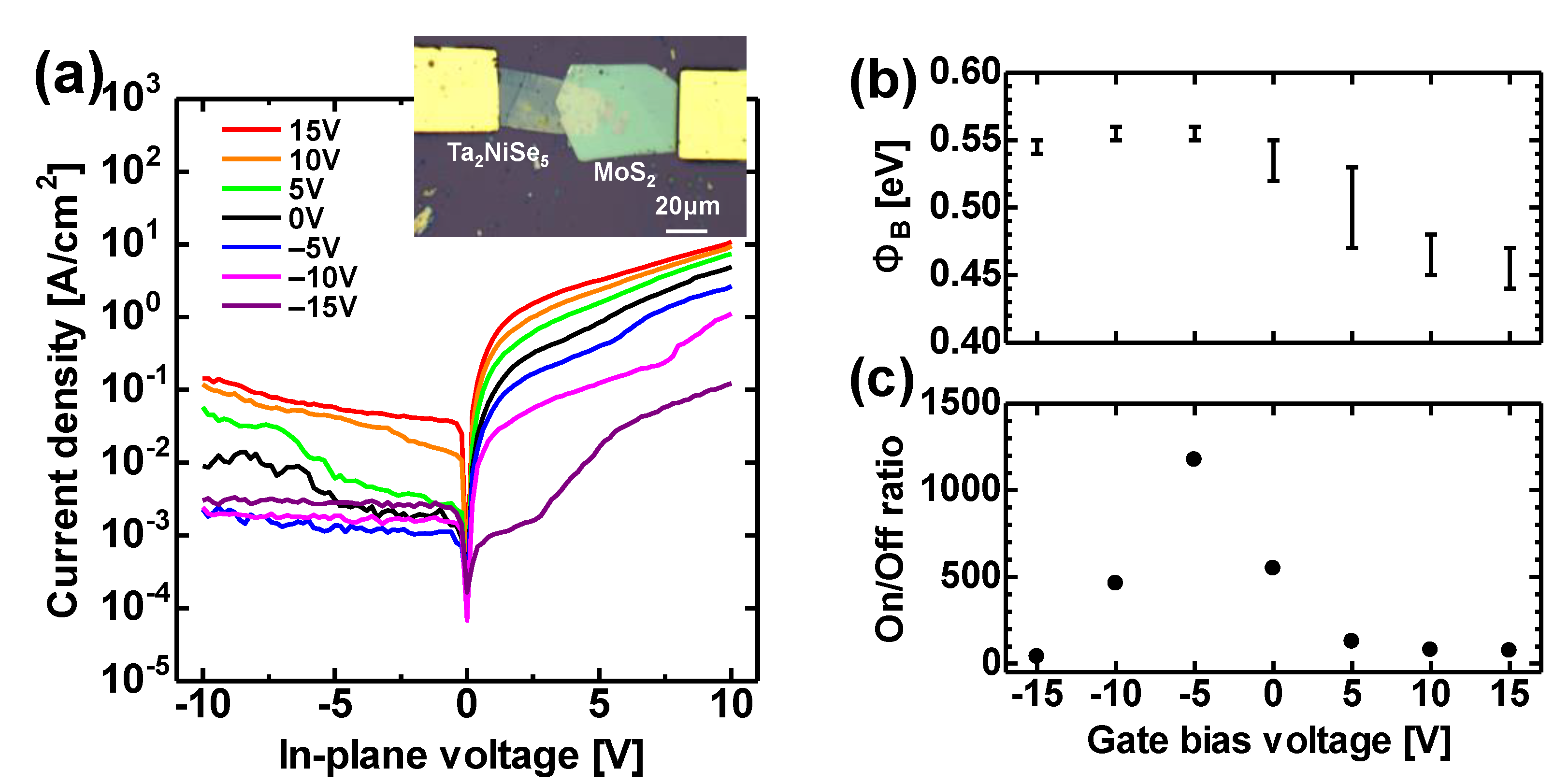
The van der Waals heterojunctions of Ta2NiSe5 with other layered materials were investigated. An unintentionally doped n-type MoS2 film was transferred onto a Ta2NiSe5 film on a SiO2/Si substrate using a polymer sheet [24]. Figure 4a shows the current density-voltage (J-V) characteristics of the MoS2/Ta2NiSe5 heterojunctions, where bias voltage was applied to the Ta2NiSe5 contact with respect to the MoS2 contact. A back-gate bias was also applied. The inset of Figure 4a shows optical microscopy images of the MoS2/Ta2NiSe5 heterojunction, where the device is assumed to have a junction area of 330 × 10−8 cm2. A diode-like rectifying behavior with a turn-on voltage of approximately 0.4 V was achieved. The current density depended on the gate bias voltage, indicating modulation of the barrier height. Figure 4b shows the gate bias voltage dependence of the barrier height at the MoS2/Ta2NiSe5 heterointerface, which was estimated using the Richardson-Dushman equation,
where J is the current density, A* = 4πm*k2q/h3 is the effective Richardson constant, m* is the hole effective mass, h is the Planck constant, ΦB is the barrier height, n is the empirical ideality factor, and V is the applied bias voltage. Figure 4c shows that the rectification (on/off) ratio depends on the gate bias voltage, defined as the ratio of the forward/reverse current density. The barrier height decreased slightly as the gate bias increased. The gate bias voltage corresponding to the maximum on/off ratio was −5 V. This is because the band alignment is modulated by tuning the Fermi level [25]. In our results, the carrier transport contributing to the current was exhibited in the band-to-band flow. In the case of an incomplete heterojunction, the J-V characteristic had a relatively high turn-on voltage, as shown in Figure S4 in the Supplementary Materials, owing to tunneling transport through a relatively large van der Waals gap [26]. Compared to the heterojunction with the complete interface, the current density decreased in all voltage ranges, and the on/off ratio remained unchanged. The tunneling transport of heterojunctions can be stably controlled by inserting hexagonal boron nitride as a thin insulator at the interface [27], and is expected to exhibit high device performance (Figure S5 in the Supplementary Materials).
4. Conclusions
The electronic properties and formation of heterojunction devices for Ta2NiSe5 films were investigated. The majority carriers were holes, as determined by the Hall effect measurement. The activation energy estimated from the temperature dependence of the carrier concentration was 0.17 eV at approximately 300 K, which is close to half of the apparent energy bandgap of the excitonic insulator state. In addition, the activation energy was 0.12 eV at approximately 400 K, indicating an unstable exciton state due to thermal fluctuation. The temperature dependence of Hall mobility below the critical temperature of an excitonic insulator nearly follows the usual temperature dependence observed in conventional semiconductor materials. The van der Waals heterojunction of the MoS2/Ta2NiSe5 structure was demonstrated. Diode-like J-V characteristics, depending on the gate bias voltage, were achieved. The barrier height at the MoS2/Ta2NiSe5 heterointerface and the on/off ratio were modulated by applying a gate bias voltage, suggesting that the carrier transport was exhibited in band-to-band flow. Our demonstration suggests that the knowledge of Ta2NiSe5 increased as an electronic material, and diode performance was successfully achieved for the electronic device applications.
Supplementary Materials
The following materials are available online at https://www.mdpi.com/article/10.3390/coatings11121485/s1: Figure S1: crystal structure and band diagram of layered Ta2NiSe5; Figure S2: the chemical bond state characterized by X-ray photoelectron spectroscopy (PHI Quantera IITM, ULVAC-PHI Inc.); Figure S3: transfer characteristic of back-gate Ta2NiSe5 field-effect device; Figure S4: current density-voltage (J-V) curve of the MoS2/Ta2NiSe5 heterojunction with incomplete interface; Figure S5: J-V curve of the MoS2//h-BN/Ta2NiSe5 heterojunction with incomplete interface.
Author Contributions
Conceptualization, N.U. and Y.H.; methodology, M.F. and N.U.; validation, M.F., N.U. and Y.H.; formal analysis, M.F. and N.U.; investigation, M.F. and N.U.; resources, N.U.; data curation, M.F. and N.U.; writing—original draft preparation, N.U.; writing—review and editing, N.U. and Y.H.; supervision, Y.H.; project administration, N.U. All authors have read and agreed to the published version of the manuscript.
Funding
This research received no external funding.
Institutional Review Board Statement
Not applicable.
Informed Consent Statement
Not applicable.
Data Availability Statement
The data that support the findings of this study are available from the corresponding author upon reasonable request.
Acknowledgments
A part of this work was carried out using the analysis facilities at the Global Aqua Innovation Center (AICS) at Shinshu University.
Conflicts of Interest
The authors declare no conflict of interest.
References
- Akinwande, D.; Huyghebaert, C.; Wang, C.-H.; Serna, M.I.; Goossens, S.; Li, L.-J.; Wong, H.-S.P.; Koppens, F.H.L. Graphene and two-dimensional materials for silicon technology. Nature 2019, 573, 507–518. [Google Scholar] [CrossRef] [PubMed]
- Zhang, E.; Wang, W.; Zhang, C.; Zhu, G.; Sun, Q.; Zhang, D.W.; Zhou, P.; Xiu, F. Tunable charge-trap memory based on few-layer MoS2. ACS Nano 2015, 9, 612–619. [Google Scholar] [CrossRef] [Green Version]
- Li, M.-Y.; Shi, Y.; Cheng, C.-C.; Lu, L.-S.; Lin, Y.-C.; Tang, H.-L.; Tsai, M.-L.; Chu, C.-W.; Wei, K.-H.; He, J.-H.; et al. Epitaxial growth of a monolayer WSe2-MoS2 lateral p-n junction with an atomically sharp interface. Science 2015, 349, 524–528. [Google Scholar] [CrossRef] [Green Version]
- Deng, W.; You, C.; Chen, X.; Wang, Y.; Li, Y.; Feng, B.; Shi, K.; Chen, Y.; Sun, L.; Zhang, Y. High-performance photodiode based on atomically thin WSe2/MoS2 nanoscroll integration. Small 2019, 15, 1901544. [Google Scholar] [CrossRef]
- Wang, J.; Jiang, Y.; Hu, Z. Dual-band and polarization-independent infrared absorber based on two-dimensional black phosphorus metamaterials. Opt. Express 2017, 25, 22149–22157. [Google Scholar] [CrossRef]
- Qiu, C.; Wu, J.; Zhu, R.; Shen, L.; Zheng, B. Dual band near-perfect metamaterial absorber based on cylinder MoS2-dielectric arrays for sensors. Opt. Commun. 2019, 451, 226–230. [Google Scholar] [CrossRef]
- Kenari, M.A. Printed planer patch antennas based on metamaterial. Int. J. Electron. Lett. 2013, 2, 37–42. [Google Scholar] [CrossRef]
- Kenari, M.A.; Virdee, B.S.; Limiti, E. Wideband planer array antenna based on SCRLH-TL for air borne synthetic aperture radar application. J. Electromagn. Waves Appl. 2018, 32, 1586–1599. [Google Scholar] [CrossRef]
- Althuwayb, A.A. Enhanced radiation gain and efficiency of a metamaterial-inspired wideband microstrip antenna using substrate integrated waveguide technology for sub-6 GHz wireless communication systems. Microw. Opt. Technol. Lett. 2021, 63, 1892–1898. [Google Scholar] [CrossRef]
- Das, S.; Robinson, J.A.; Dubey, M.; Terrones, H.; Terrones, M. Beyond graphene: Progress in Novel two-dimensional materials and van der waals solids. Annu. Rev. Mater. Res. 2015, 45, 1–27. [Google Scholar] [CrossRef]
- Kobayashi, Y.; Mori, S.; Maniwa, Y.; Miyata, Y. Bandgap-tunable lateral and vertical heterostructures based on monolayer Mo1-xWxS2 alloys. Nano Res. 2015, 8, 3261–3271. [Google Scholar] [CrossRef]
- Saito, Y.; Nojima, T.; Iwasa, Y. Highly crystalline 2D superconductors. Nat. Rev. Mater. 2017, 2, 16094. [Google Scholar] [CrossRef] [Green Version]
- Mak, K.F.; Shan, J.; Palph, D.C. Probing and controlling magnetic states in 2D layered magnetic materials. Nat. Rev. Phys. 2019, 1, 646–661. [Google Scholar] [CrossRef]
- Di Salvo, F.J.; Chen, C.H.; Fleming, R.M.; Waszczak, J.V.; Dunn, R.G.; Sunshine, S.A.; Ibers, J.A. Physical and structural properties of the new layered compounds Ta2NiS5 and Ta2NiSe5. J. Less Common Met. 1986, 116, 51–61. [Google Scholar] [CrossRef]
- Nakano, A.; Hasegawa, T.; Tamura, S.; Katayama, N.; Tsutsusi, S.; Sawa, H. Antiferroelectric distortion with anomalous phonon softening in the excitonic insulator Ta2NiSe5. Phys. Rev. B 2018, 98, 045139. [Google Scholar] [CrossRef] [Green Version]
- Wakisaka, Y.; Sudayama, T.; Takubo, K.; Mizokawa, T.; Arita, M.; Namatame, H.; Taniguchi, M.; Katayama, N.; Nohara, M.; Takagi, H. Excitonic insulator state in Ta2NiSe5 probed by photoemission spectroscopy. Phys. Rev. Lett. 2009, 103, 026402. [Google Scholar] [CrossRef] [PubMed]
- Nakano, A.; Nagai, T.; Katayama, N.; Sawa, H.; Taniguchi, H.; Terasaki, I. Exciton transport in the electron-hole system Ta2NiSe5. J. Phys. Soc. Jpn. 2019, 88, 113706. [Google Scholar] [CrossRef]
- Li, L.; Wang, W.; Gan, L.; Zhou, N.; Zhu, X.; Zhang, Q.; Li, H.; Tian, M.; Zhai, T. Ternary Ta2NiSe5 flakes for a high-performance infrared photodetector. Adv. Funct. Mater. 2016, 26, 8281–8289. [Google Scholar] [CrossRef]
- Qiao, J.; Feng, F.; Wang, Z.; Shen, M.; Zhang, G.; Yuan, X.; Somekh, M.G. Highly in-plane anisotropic two-dimensional ternary Ta2NiSe5 for polarization-sensitive photodetectors. ACS Appl. Mater. Interfaces 2021, 13, 17948–17956. [Google Scholar] [CrossRef] [PubMed]
- Kim, S.Y.; Kim, Y.; Kang, C.-J.; An, E.-S.; Kim, H.K.; Eom, M.J.; Lee, M.; Park, C.; Kim, T.-H.; Choi, H.C.; et al. Layer-confined excitonic insulating phase in ultrathin Ta2NiSe5 crystals. ACS Nano 2016, 10, 8888–8894. [Google Scholar] [CrossRef]
- Yan, J.; Xiao, R.; Luo, X.; Lv, H.; Zhang, R.; Sun, Y.; Tong, P.; Lu, W.; Song, W.; Zhu, X.; et al. Strong Electron-phonon coupling in the excitonic insulator Ta2NiSe5. Inorg. Chem. 2019, 58, 9036–9042. [Google Scholar] [CrossRef] [PubMed]
- Lu, Y.F.; Kono, H.; Larkin, T.I.; Rost, A.W.; Takayama, T.; Boris, A.V.; Keimer, B.; Takagi, H. Zero-gap semiconductor to excitonic insulator transition in Ta2NiSe5. Nat. Commun. 2017, 8, 14408. [Google Scholar] [CrossRef] [PubMed]
- Mao, J.; Shuai, J.; Song, S.; Wu, Y.; Dally, R.; Zhou, J.; Liu, Z.; Sun, J.; Zhang, Q.; dela Cruz, C.; et al. Manipulation of ionized impurity scattering for achieving high thermoelectric performance in n-type Mg3Sb2-based materials. Proc. Natl. Acad. Sci. USA 2017, 114, 10548–10553. [Google Scholar] [CrossRef] [Green Version]
- Wakafuji, Y.; Moriya, R.; Masubuchi, S.; Watanabe, K.; Taniguchi, T.; Machida, T. 3D manipulation of 2D materials using microdome polymer. Nano Lett. 2020, 20, 2486–2492. [Google Scholar] [CrossRef]
- Deng, Y.; Luo, Z.; Conrad, N.J.; Liu, H.; Gong, Y.; Najmaei, S.; Ajayan, P.M.; Lou, J.; Xu, X.; Ye, P.D. Black phosphorus-monolayer MoS2 van der Waals Heterojunction p-n diode. ACS Nano 2014, 8, 8292–8299. [Google Scholar] [CrossRef] [PubMed] [Green Version]
- Tan, C.; Yin, S.; Chen, J.; Lu, Y.; Wei, W.; Du, H.; Liu, K.; Wang, F.; Zhai, T.; Li, L. Broken-Gap PtS2/WSe2 van der Waals Heterojunction with Ultrahigh Reverse Rectification and Fast Photoresponse. ACS Nano 2021, 15, 8328–8337. [Google Scholar] [CrossRef]
- Jeong, H.; Bang, S.; Oh, H.M.; Jeong, H.J.; An, S.-J.; Han, G.H.; Kim, H.; Kim, K.K.; Park, J.C.; Lee, Y.H.; et al. Semiconductor-insulator-semiconductor diode consisting of monolayer MoS, h-BN, and GaN heterostructure. ACS Nano 2015, 9, 10032–10038. [Google Scholar] [CrossRef] [PubMed]
Figure 1.
Schematic of the experimental setup for the preparation of Ta2NiSe5.
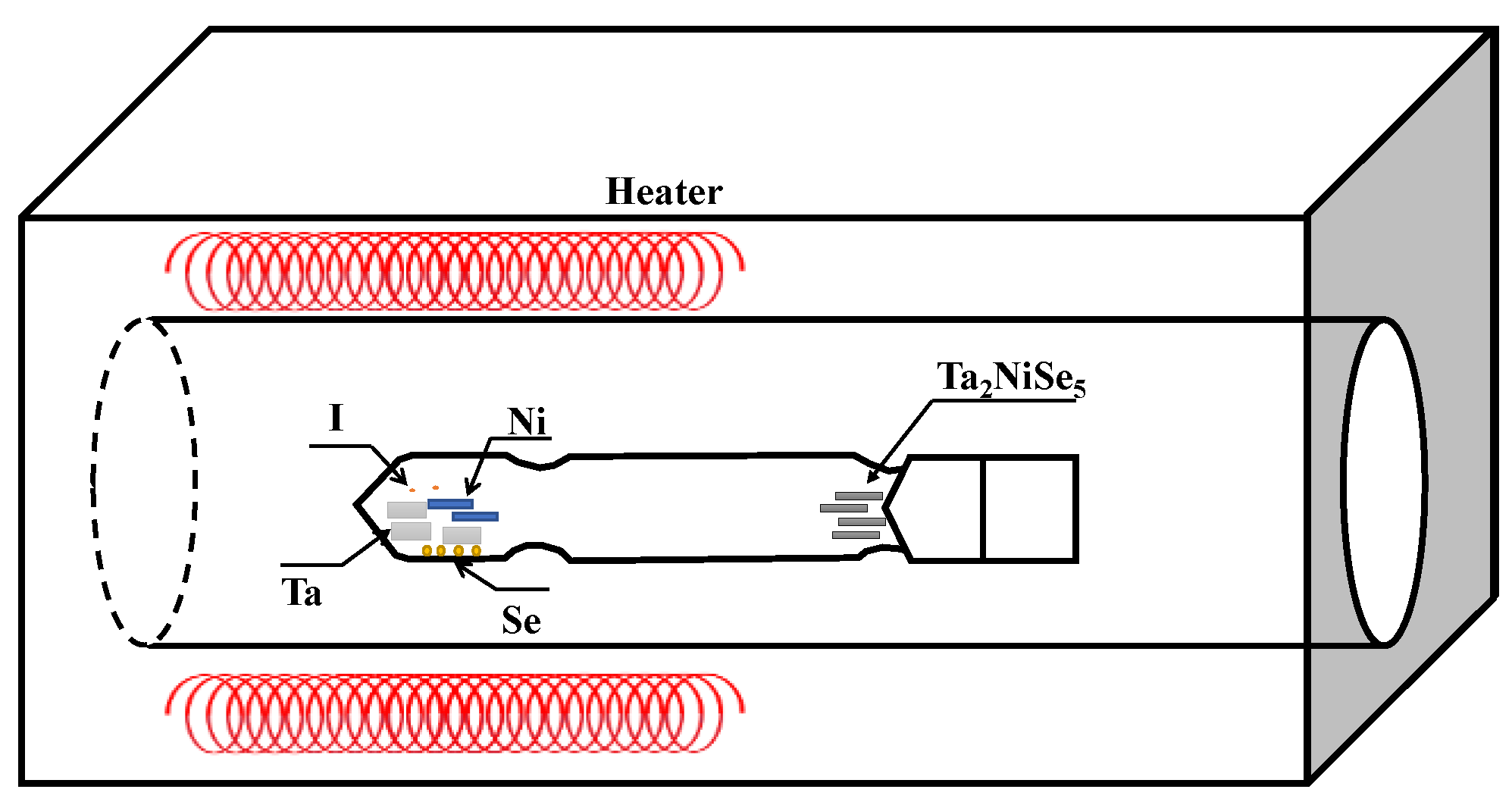
Figure 2.
(a) SEM image of the Ta2NiSe5 film with elemental analysis of EDX; (b) Raman spectrum of the Ta2NiSe5 film.
Figure 2.
(a) SEM image of the Ta2NiSe5 film with elemental analysis of EDX; (b) Raman spectrum of the Ta2NiSe5 film.
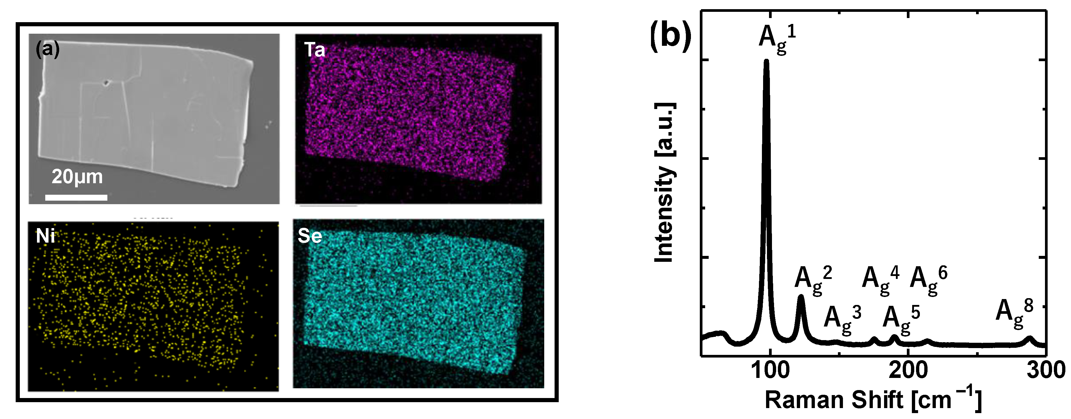
Figure 3.
Temperature dependence of (a) carrier concentration and (b) Hall mobility for different thicknesses of Ta2NiSe5 films. The inset of (a) presents an enlarged view of the data near the Tc (328 K, 3.05 K−1) of the excitonic insulator transition.
Figure 3.
Temperature dependence of (a) carrier concentration and (b) Hall mobility for different thicknesses of Ta2NiSe5 films. The inset of (a) presents an enlarged view of the data near the Tc (328 K, 3.05 K−1) of the excitonic insulator transition.

Figure 4.
(a) J-V characteristics of the MoS2/Ta2NiSe5 heterojunction depending on gate bias voltage; (b) barrier height at the MoS2/Ta2NiSe5 heterointerface; and (c) rectification ratio depending on gate bias voltage.
Figure 4.
(a) J-V characteristics of the MoS2/Ta2NiSe5 heterojunction depending on gate bias voltage; (b) barrier height at the MoS2/Ta2NiSe5 heterointerface; and (c) rectification ratio depending on gate bias voltage.
Publisher’s Note: MDPI stays neutral with regard to jurisdictional claims in published maps and institutional affiliations. |
© 2021 by the authors. Licensee MDPI, Basel, Switzerland. This article is an open access article distributed under the terms and conditions of the Creative Commons Attribution (CC BY) license (https://creativecommons.org/licenses/by/4.0/).
Share and Cite
MDPI and ACS Style
Fukai, M.; Urakami, N.; Hashimoto, Y. Electrical Properties in Ta2NiSe5 Film and van der Waals Heterojunction. Coatings 2021, 11, 1485. https://doi.org/10.3390/coatings11121485
AMA Style
Fukai M, Urakami N, Hashimoto Y. Electrical Properties in Ta2NiSe5 Film and van der Waals Heterojunction. Coatings. 2021; 11(12):1485. https://doi.org/10.3390/coatings11121485
Chicago/Turabian StyleFukai, Masaya, Noriyuki Urakami, and Yoshio Hashimoto. 2021. "Electrical Properties in Ta2NiSe5 Film and van der Waals Heterojunction" Coatings 11, no. 12: 1485. https://doi.org/10.3390/coatings11121485
Note that from the first issue of 2016, this journal uses article numbers instead of page numbers. See further details here.