Article

Tuning the Surface Characteristic of Al-Si Alloys and Its Impacts on the Formation of Micro Arc Oxidation Layers

1
School of Materials Science and Engineering, Dongguan University of Technology, Dongguan 523808, China
2
Shenzhen Institute of Advanced Technology, Chinese Academy of Sciences, Shenzhen 518055, China
*
Authors to whom correspondence should be addressed.
Coatings 2021, 11(4), 453; https://doi.org/10.3390/coatings11040453
Submission received: 7 March 2021 / Revised: 5 April 2021 / Accepted: 12 April 2021 / Published: 14 April 2021

Abstract

:
Aluminum Silicon (Al-Si) alloys are the most important among cast alloys and have widespread application. The β-Si phase is detrimental to the growth of micro arc oxidation (MAO) layers on Al-Si alloys. In this paper, the β-Si in the skin layer of different Al-Si alloys was removed by an acid etching pretreatment. Then, the impacts of different etching condition on their MAO process were investigated. Results show that, as etching time was prolonged, the Si content on the surface of Al-12 Si was decreased greatly (less than 0.5 wt.%), and the average size of pores left on the sample surface was increased gradually. This then led to the occurrence of some bigger and more drastic discharge sparks at the earlier oxidation stage. The corresponding layers had a higher ratio of Al2O3 and better corrosion resistance after 30 min of oxidation. Moreover, a 60 s etching pretreatment benefitted and boosted the growth rate and energy efficiency of layers on the Al-9 Si, Al-12 Si and Al-15 Si alloys. Such pretreatment was believed to be applicable to restrain the negative effects of Si on the MAO of different Al-Si alloys.

1. Introduction

Al-Si alloys have wide application in the manufacturing of various machinery parts and components, due to their prominent properties, such as high specific strength, low thermal expansion, good castability, low costs, etc. [1,2]. Recently, some Al-Si alloys with near-eutectic compositions, e.g., AlSi10Mg and AlSi12, were considered as prospective materials in the additive manufacturing of aluminum alloy products [3]. However, poor wear resistance and corrosion resistance are obstacles for the application of Al-Si alloys in some harsh working conditions. Therefore, surface modification is usually necessary for many Al-Si alloy products. Laser cladding, thermal spraying, anodic oxidation, and micro-arc oxidation (i.e., plasma electrolytic oxidation) are effective technologies to enhance the surface performance of Al-Si alloys [4,5,6,7]. Among them, anodic oxidation and micro-arc oxidation (MAO) are powerful approaches to deposit strong joint-strength layers on workpieces with complex shapes. However, the presence of the Si phase makes it difficult to form a uniform anodic film on the surface of Al-Si alloys. This is because it is difficult to oxidize β-Si under a low temperature, which eventually exists in the alumina film as an inclusion and degrades the film property [8,9]. Fortunately, in the MAO process, the local temperature will rocket to more than 3000 K under the promotion of discharge sparks. The ultrahigh temperature on the local surface of the workpiece promotes violent oxidation of both the β-Si and α-Al phase, and leads to a ceramic layer in-situ growing on the surface of Al-Si alloys. Besides, as a simple and eco-friendly technique, the MAO can fabricate coatings with high performance, e.g., high hardness, good anticorrosion and wear resistance [10,11]. In this regard, the MAO technique is more suitable for the surface strengthening of Al-Si alloys [12,13,14]. However, big eutectic or primary Si phase in Al-Si alloys would act as barriers for the growth of the MAO layer and induce some porous mullite into the layer as well. The formation of the porous mullite deteriorates the performance of the coatings severely [15,16,17]. To this end, some special methods, such as β-Si refinement, pre-anodization, and sealing post-treatment, were developed to improve the performance of MAO layers on Al-Si alloys [18,19,20]. However, the efficiency of the above methods is not desirable, as they cannot solve the problems of β-Si radically. In view of the fact that pretreatment, such as shot-peening, high temperature oxidation prefab film, etc., can change the surface structure, stress or composition of aluminum alloys, their MAO process and layer performance would be affected [21,22]. Removing the large Si phase before MAO treatment of Al-Si alloy is supposed to achieve a fine layer.
In this paper, an acid etching pretreatment was applied to remove the β-Si in the skin layer of Al-Si alloys, and the impacts of acid composition and etching time on the MAO process of Al-Si alloys were studied systematically. Moreover, the relationship between surface condition variation and discharge spark morphology was discussed.

2. Experiments

2.1. Layer Fabrication

The experiment material was commercial pure Al (Al ≥ 99.7 wt.%) and Al-Si casting alloys with Si content of 9, 12, and 15 wt.%. These Al-Si alloys were assigned as Al-9 Si, Al-12 Si and Al-15 Si, respectively. The samples (20 mm × 20 mm × 4 mm) were polished with 1000 grit sandpaper. The etching acid was composed of HF (40 wt.%) and HNO3 (65 wt.%) with a volume ratio of 1: 4. Some samples was immersed entirely into the acid to remove the β-Si phase in the skin layer. Before the MAO treatment, all samples were cleaned by distilled water, ultrasonic cleaned in acetone, and then blew dry. The electrolyte was composed of 10 g/L Na2SiO3, 2 g/L NaOH and 2 g/L C6H12N4. A bipolar pulse power (WHD60, Harbin, China) was applied for MAO processing. The morphology of discharge sparks on the sample surface was recorded by a high-speed digital camera.

2.2. Layer Characterization

The microstructure of the MAO coating was characterized by a field emission scanning electron microscope (Nano 430, Hillsboro, OR, USA), and the composition was detected by an energy dispersive spectrometer (INCA, Morgantown, VA, USA). The layer thickness was the average value of 10 points measured by measured by a Surfix N eddy current thickness meter. The phase structures of the coated samples were determined by an X-ray diffractometer (Rigaku Miniflex 600, Tokyo, Japan), using Cu-Kα radiation as the excitation source. The scanning range was 20° to 70° (in 2θ), with a step size of 0.02°. The electrochemical behavior of the samples was tested by an electrochemical workstation (CHI660D, Shanghai, China) with 3.5 wt. % NaCl solution. Before the polarization measurements, all samples were immersed in the NaCl solution for about 20 min until the OCP was stable. The abrasion performance of the MAO layer was measured by a ball-on-disk wear tester (MS-T3000, Lanzhou, China), with a WC-6CO alloy ball (φ3 mm) as friction pair and a load of 3 N. The dry friction time was 20 min with a rotation speed of 120 r/min. The weight of each sample before and after wear was measured by a high precision electronic balance (0.01 mg).

3. Results and Discussions

3.1. Effects of Etching Time on the MAO of Al-12 Si Alloy

The Si content in the surface layer of eutectic Al-Si alloy treated by different etching time is shown in Figure 1. For the pristine sample, the Si content on its surface was a bit higher than in the bulk; in that, the Si was harder than Al, and more difficult to eliminate by grinding. When the substrates were subjected to a 15 s etching treatment, the Si content on its surface declined greatly to about 2 wt.%; this is because the Si was mostly removed while the Al was preserved by a thin passivation layer [23]. As the etching time extending to 30 s, more Si phase in the deeper layer was removed and the Si content on the surface approached 0.7 wt.%. Henceforth, the Si content in the surface layer of the matrix almost kept stable, even when the etching time was further extended. Eventually, the content of Si was about 0.5 wt.% when the sample was etched for 60 s.
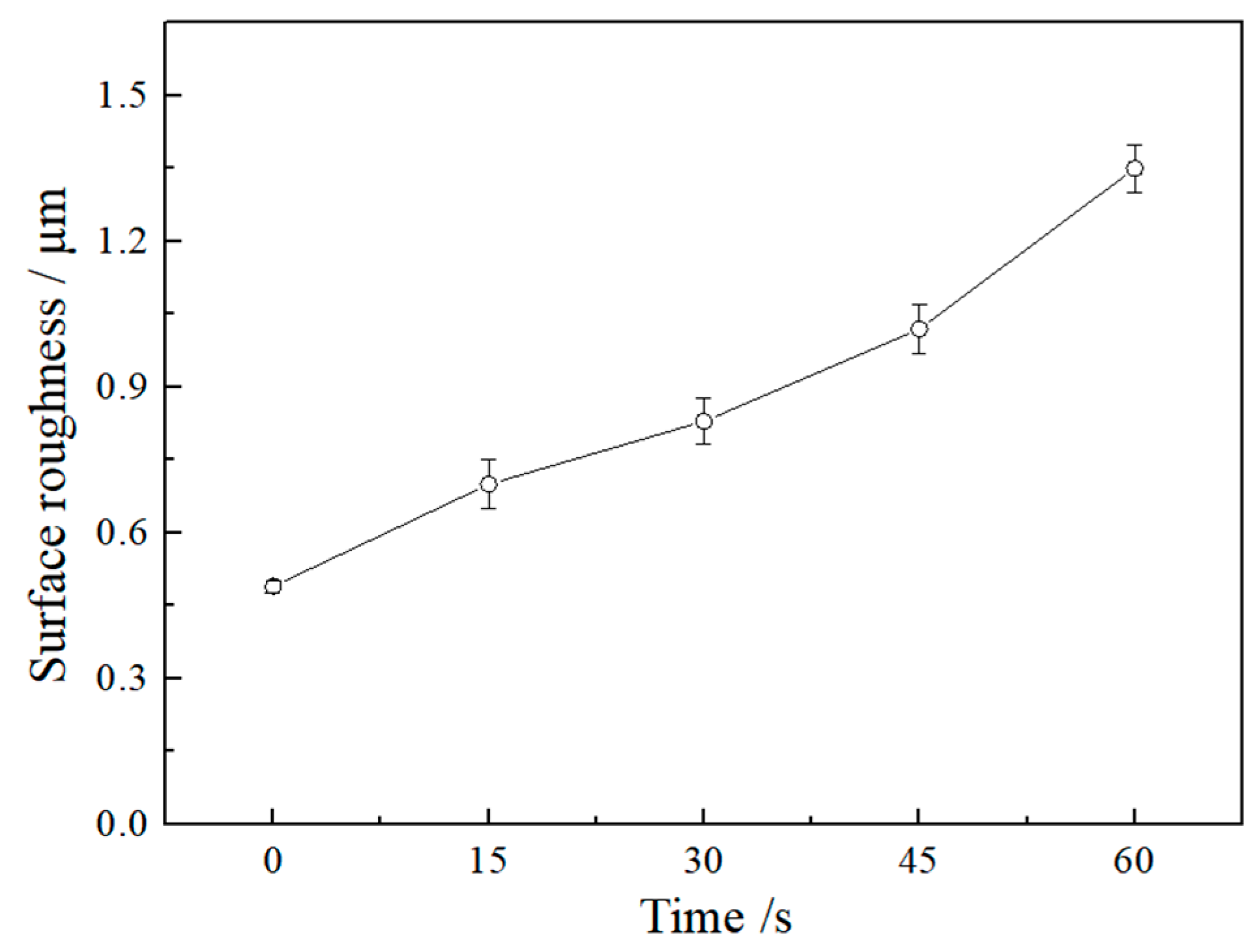
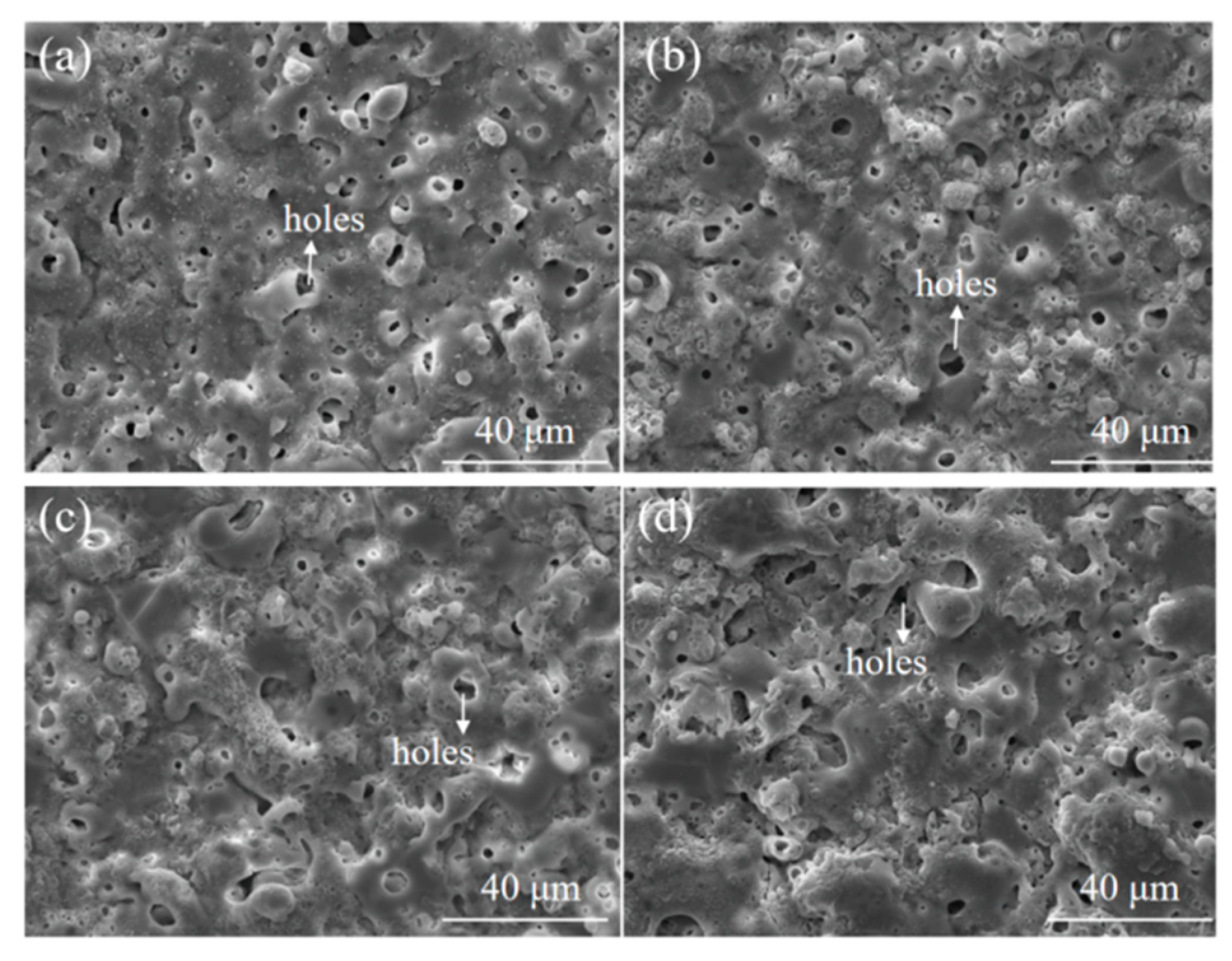
Figure 2 shows the surface morphology of the Al-12 Si matrix after different etching times. The substrate surface was flat after the polishing process. However, abundant small worm-like holes and a few large pits were observed on the surface after the immersion of the alloys in the mixed acid. This is because the eutectic and primary Si phase can be dissolved by HF, whereas the α-Al was reserved due to the formation of the passivation layer in the presence of HNO3. Though the Si content on the sample surface just decreased from 2.1 to 0.5 wt.%, as the etching time extending from 15 to 60 s, the volume of pores left by the original β-Si was increased gradually, and the corresponding surface roughness increased from 0.7 to 1.35 μm (Figure 3). When the matrix was etched for more than 30 s, some holes on their surface were extremely large, with a width of several microns and a length of dozens of microns. The reason may be that the INCA just detected the elements within a small depth on the sample surface, though the Si at a much deeper range was further dissolved as the acid etching time extended.
Figure 4 shows the discharge sparks’ morphology at the oxide/electrolyte interface by different MAO time. Actually, feeble sparks were observed by the naked eye on the etched Al-12 Si just 1 min after the beginning of oxidation, when the positive voltage reached about 170 V. However, tiny sparks started to appear on the non-etched sample after about 3 min of oxidation, when the voltage was about 190 V. As the positive voltage increased, the luminance and size of discharge sparks both increased. However, the shape of the sparks on all samples was much different. At the same moment, the luminance and size of most sparks on different samples all increased with their etching time. For the matrix etched for 60 s, the morphology spark on its surface was a bit special from the 5th min of oxidation, as some discharge sparks on its surface were particularly dazzling. As the oxidation carried on, the average size and brightness of discharge sparks increased, while their number diminished gradually. The sparks on the etched sample were always fiercer than that on the non-etched one. Table 1 shows the positive voltage and layer thickness of different samples by the 20th and 30th min of oxidation. The etching pretreatment led to a higher voltage and a thicker layer on the Al-12 Si. With the extension of etching time from 15 to 60 s, the positive voltage of the substrates decreased, while the layer thickness increased gradually. These phenomena indicated that the surface structure of the matrix may play a great role in the discharge mechanism over its MAO process.
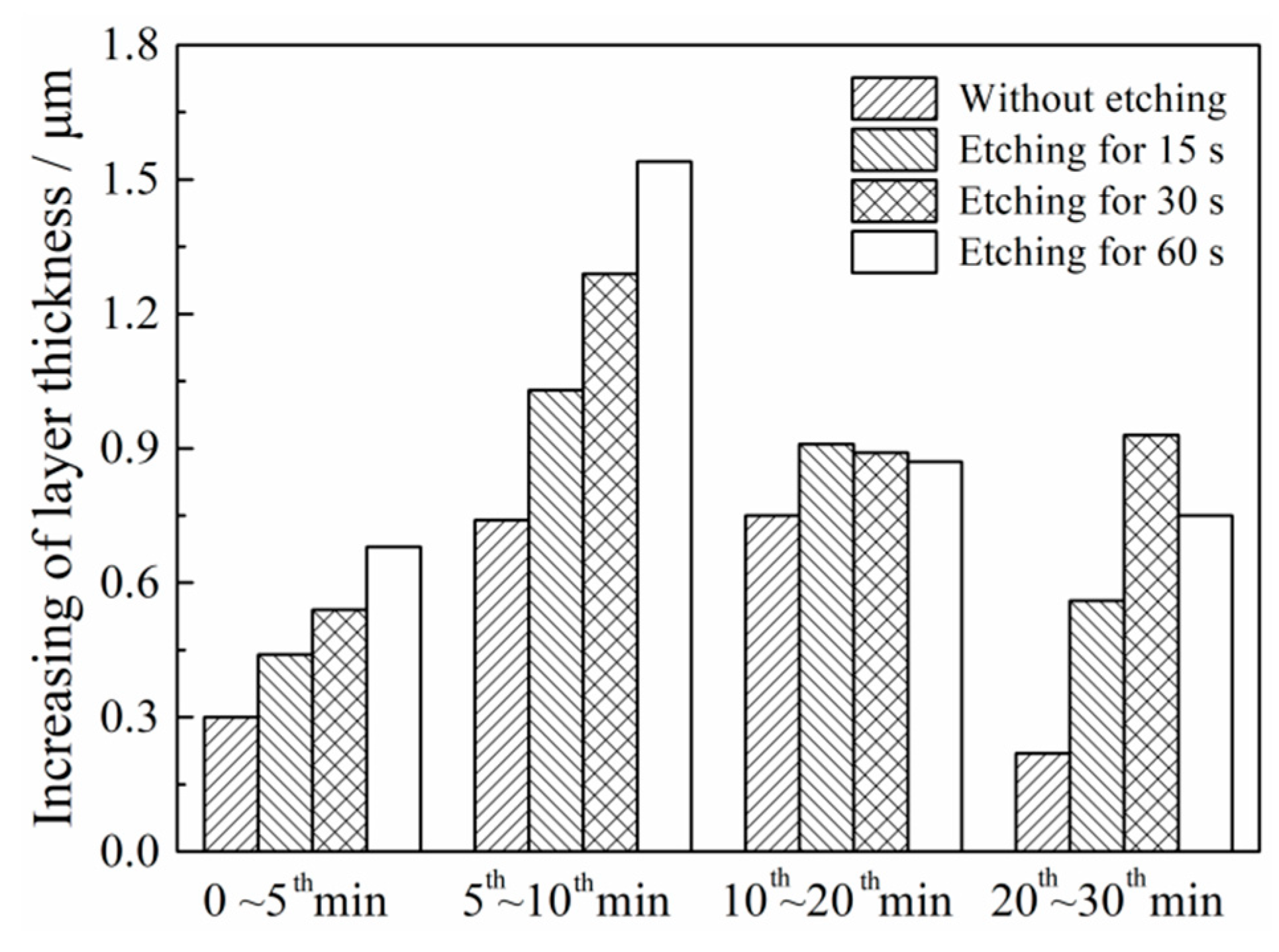
Figure 5 shows the thickness of layers that grew on different Al-12 Si during different MAO periods. The thickness of the MAO layer for all samples increased with the prolonging of etching time. During the first 10 min, the layers’ growth rate was obviously increased when the matrix etching time extending from 0 to 60 s; but, during the 5th to 10th min, each layer had a much faster growth rate compared with the case at the first 5 min. From the 10th to 20th min, the layers’ growth rate for the Al-12 Si with etching pretreatment was obviously decreased. From the 20th to 30th min, the growth rate for the layers on all samples was further decreased. For the Al-12 Si without etching pretreatment, its layer grew especially slowly. After 30 min of oxidation, the thickness of MAO layers on the Al-12 Si became thicker and thicker with the matrix etching pretreatment time. The layer on the sample with 60 s of etching was 25.6 μm, which was about 10 μm thicker than the non-etched substrates.
The surface morphology of the layers on different samples by 30 min MAO treatment is shown in Figure 6. The etching pits on the surface of Al-12 Si with the acid pretreatment disappeared. All layers demonstrated an even surface structure accompanied by some shallow holes. The surface roughness of the coated samples also increased with the extending of their etching time. This is because the volume of some sediments depositing on the surface would evidently increase when the size and intensity of the discharge sparks increased.
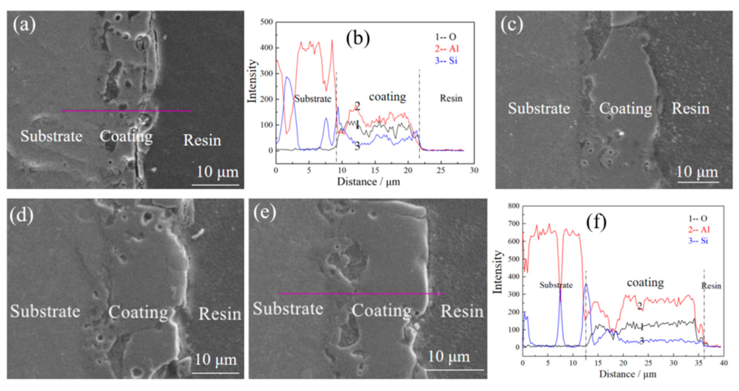
The cross-section of the above layers on Al-12 Si with different etching times and the EDS line scans for O, Al and Si, across the layers on the sample without and with 60 s, is exhibited in Figure 7. The layers’ thickness (Figure 7a,c–e) was in correspondence with the tested values as shown in Table 1. Though some big pores still existed at the inner part of the layer on the samples with etching pretreatment, the density of their outer part was significantly improved compared with the layer on sample without etching. Besides, a thin and less porous sub-layer existed near the layer/substrate interface, which implied a strong adhesion of the MAO layer to the sample surface. The composition profiles of layers on the Al-12 Si without (Figure 7b) and with 60 s (Figure 7f) etching pretreatment also imply the substrate/coating interface; Al content decreased while O content increased rapidly (Figure 7b,f). From the inner to the outer part of the coatings, the O, Al and Si contents had some big fluctuations. For the layer on the sample without etching, the Si content at most areas across the layer was high (Figure 7b). However, for the layer on the sample with 60 s etching pretreatment, the Si distribution at its middle and outer part was much more even and lower than that at its inner part (Figure 7f).
Figure 8 exhibits the phase compositions of MAO layers on Al-12 Si alloys by different oxidation time. The Al and Si peaks are from the matrix. Hence, the layers were mainly composed of γ-Al2O3, α-Al2O3, mullite, and some amorphous. With 10 min of oxidation, the intensity of the Al2O3 peak enhanced, while the mullite and amorphous peaks declined as the extension of matrix etching time. It implied that the decrease of Si mass on the surface of Al-Si alloy would contribute to the content increase of alumina in its MAO layer. With 20 or 30 min oxidation, the intensity of Al2O3 and mullite peaks both increased, while the amorphous peak receded a bit with the extension of etching time.
Figure 9 shows the potentiodynamic polarization curves and corresponding corrosion parameters of different samples. The raw Al-12 Si and different Al-12 Si samples with 30 min MAO treatment demonstrated a similar corrosion voltage, which all lay in the range of 0.68 to 0.75 V. However, the corrosion current density of the MAO treated samples was much lower than the matrix. As the value of the raw matrix was 1.21 μA/cm2 when it underwent a 30 min oxidation, the corrosion current density decreased to 0.78 μA/cm2. Besides, the value of the layers further decreased from 0.32 to 0.16 μA/cm2 with the sample etching time extending from 15 to 60 s, indicating that the decay resistance of the MAO layer was boosted more than two-times when the matrix suffered an etching pretreatment. The anticorrosion performance of MAO layers improved gradually with the prolonging of etching time.
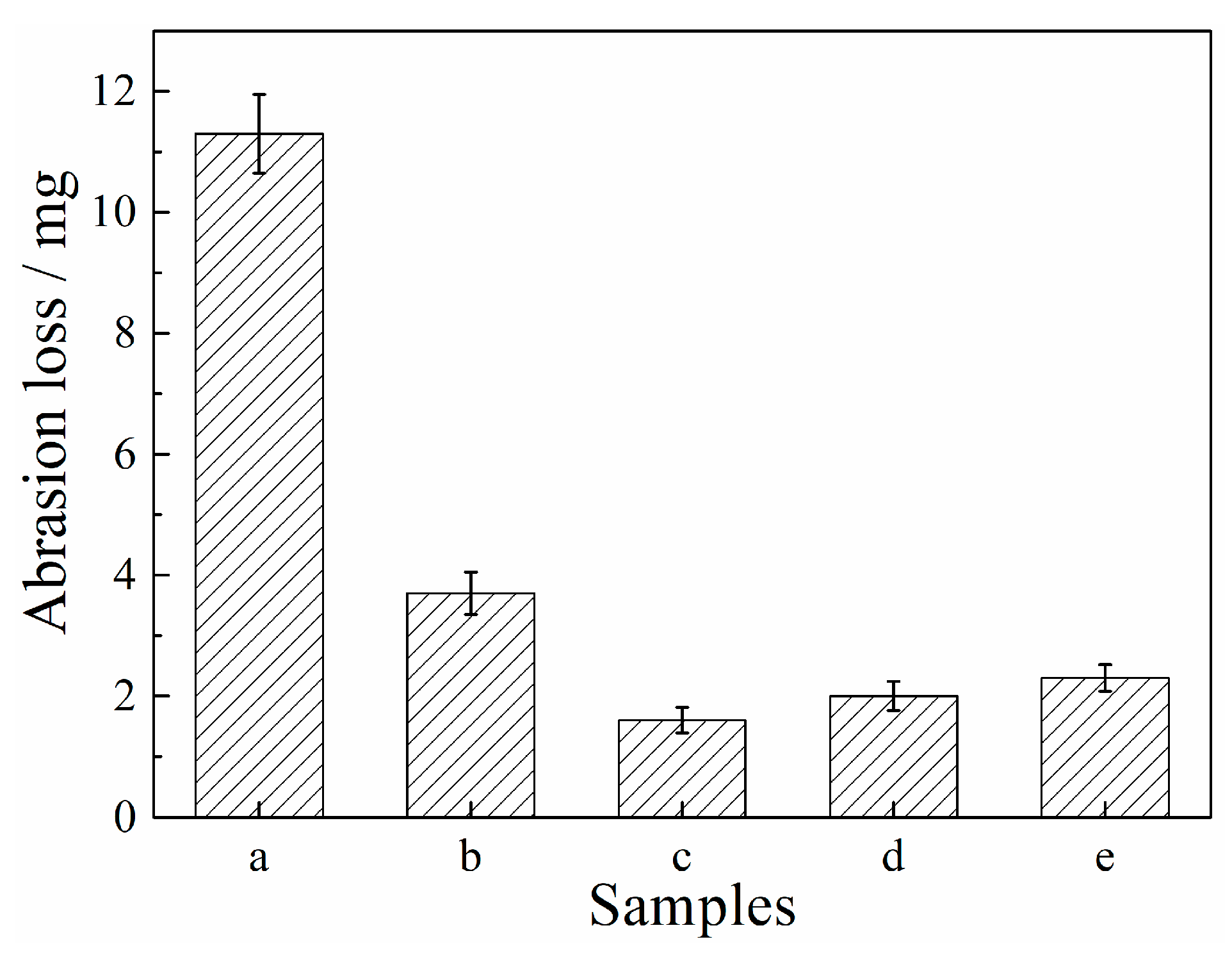
Figure 10 exhibits the weight loss of samples over the 20 min dry friction. The wear loss of the raw Al-12 Si matrix reached about 11.3 mg. However, after 30 min MAO treatment and a ceramic coating generation, its surface wear loss was significantly reduced to 3.7 mg. As for the MAO layers on the etched matrix, the wear loss further decreased. However, the corresponding value increased a bit from 1.6 to 2.3 mg as the etching time extended from 15 to 60 s.

3.2. Effects of Etching on the MAO of Hypo- and Hyper-Eutectic Al-Si Alloys

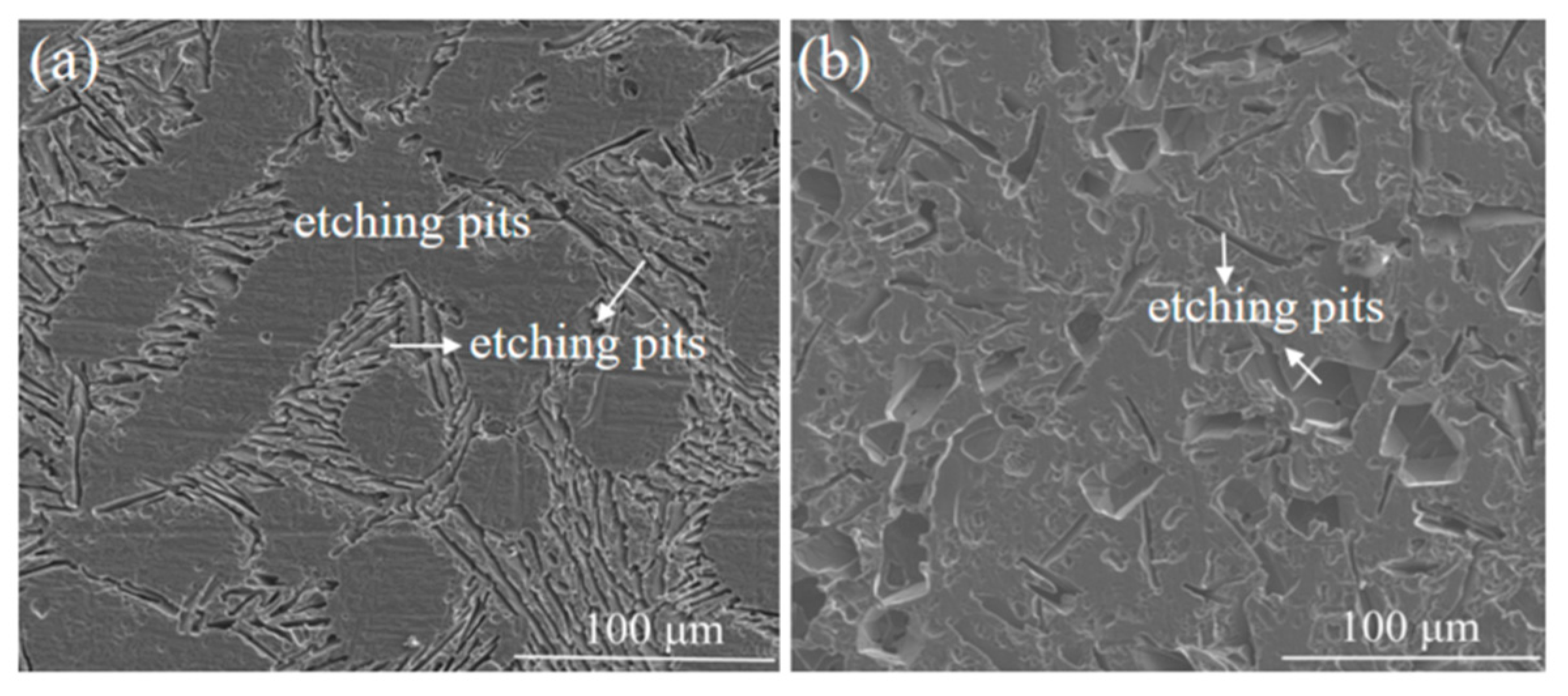
The etching time had a significant impact on the MAO process of Al-12 Si alloy, especially for the sample with 60 s etching pretreatment. Therefore, the effects of acid etching on other Al-Si alloys deserve further verification. Figure 11 presents the surface morphology of Al-9 Si and Al-15 Si by 60 s etching treatment. Plenty of strip-like pits appeared on the surface of Al-9 Si, and merely 0.5 wt.% of Si were left in the skin layer, as most eutectic Si was dissolved by the acid. Lots of blocky and some strip-like holes were generated on the surface of Al-15 Si because the majority of eutectic and primary Si were eliminated. Thus, just 1.6 wt.% of Si was left. Its residual Si content was slightly higher than that on the Al-9 Si with the same pretreatment. The reason may be that the volume of primary Si was tremendous and cannot be entirely dissolved by the acid within 60 s.
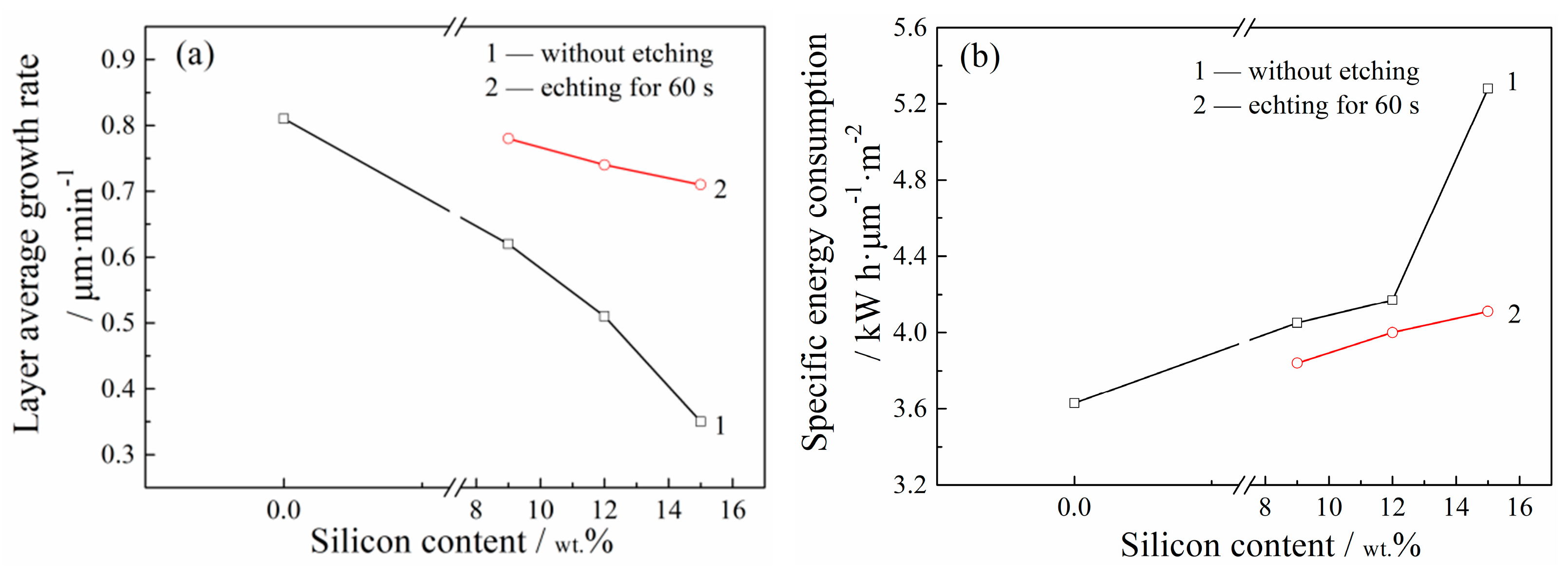
Figure 11 reveals the average growth rate and specific energy consumption of the pure Al and different Al-Si alloys with 10 min of MAO treatment. The layer deposition rate of the non-etched Al-Si alloy significantly decreased from 0.6 to 0.35 μm min−1 as the matrix Si content increased from 9 to 15 wt.% (Figure 12a). However, the value for the layers on the Al-Si alloy with 60 s etching pretreatment became much closer to each other. The average layer growth rate merely decreases from 0.76 to 0.7 μm min−1, with the Si content in the matrix increasing from 9 to 15 wt.% (Figure 12b). As to the specific energy consumption, the values of the layers on the non-etched samples increased from 4.0 to 5.3 kW h m−2 μm−1 when the Si alloys increased from 9 to 15 wt.% However, after 60 s etching pretreatment, their values all decreased. The specific energy consumption slightly increased from 3.8 to 4.0 kW h m−2 μm−1, with the increase of Si in the original matrix. Specifically for the layer on the Al-9 Si alloy with 60 s of etching, its average growth rate and specific energy consumption turned approximate to the layer on pure Al by the same MAO processing condition.

3.3. MAO Process and Discharge Mechanism Analysis

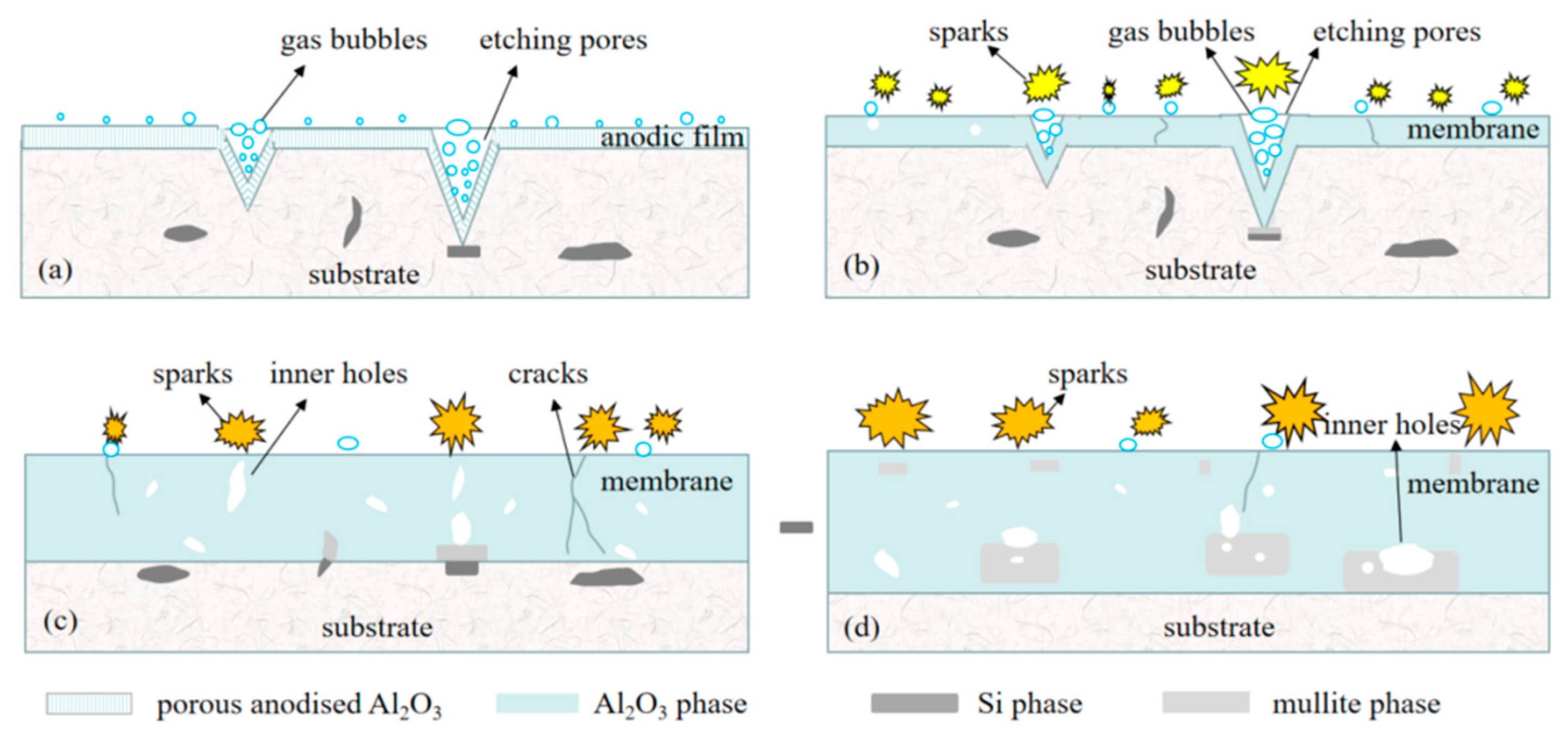
Acid etching time played a great role in the surface state of Al-Si alloys, and thus led to a peculiar discharge behavior and layer growth characteristics over the MAO process. Hence, the effects of the matrix surface structure and composition on the discharge mechanism over the whole MAO process deserve further discussion. As the layer deposition involves a series of physical and plasma chemical reactions, the analysis of spark characteristics is helpful for understanding the discharge mechanism. According to the evolution process of etching pits over the MAO process (Figure 13) and the discharge sparks morphology, we may speculate that the layer growth process of etched Al-Si alloys can be divided into four stages, as schematically shown in Figure 14.
The layer on the Al-Si alloys with etching pores on their surface started to grow by a conventional anodic oxidation (labelled as stage Ⅰ, Figure 14a). Because the β-Si on the sample with etching pretreatment was almost disappeared, the α-Al was directly exposed to the electrolyte. Thus, an alumina film could successfully grow on almost the whole sample surface, specifically, in the sample with a long etching time (60 s), the big sunk pores significantly expanded the surface area of Al. Consequently, the electrical resistance of these coated samples rapidly increased. Besides, the leakage current passed through the surface of semiconductor Si or thin SiO2 was also reduced with the decrease of β-Si on the sample surface. That is, more electric energy could be utilized for film deposition [24]. The energy efficiency over the MAO of Al-Si alloys improved gradually with the prolonging of matrix etching time.
The sparks began to emerge on the sample surface and the layer growth came into stage Ⅱ (Figure 14b) when the etching pits were gradually filled by the oxidative products, which can be seen in Figure 13a,b. The size and brightness of sparks increased as the oxidation went on. At the fifth minute of oxidation, some sparks on the surface of etched samples became noticeably larger, with a size of about 0.2~1 mm; these were in line with the scale of the primal etching pits. However, the size of the etching pits was just about one-tenth of the sparks. The reason may relate to micro discharge formation manner. As lots of tiny gas bubbles generated inside the etching pits, they gathered gradually during the floating process and turned into some big bubbles at the pitheads of the pores. According to the viewpoint of Yerokhin, the glow discharge ignition in the gaseous media at the oxide/electrolyte interface was the main discharge mode over the MAO process [25]. The sample with a longer etching time had many larger pits; therefore, the gaseous media generated at these pitheads was bigger, which would result in the formation of some larger and brighter sparks, correspondingly. Thus, regarding the substrate that was subjected to 60 s etching treatment and oxidized for 5~10 min, some sparks on its surface were 10 times larger than the size of primal etching pits (about 10~50 μm). Moreover, the layer grew mainly outwards from the sample surface at this period, and the low thermal dynamics caused by the weaker sparks were still unable to convert the β-Si below the α-Al and the SiO32− in the electrolyte into SiO2 [7,26]. That is, the Al from the surface of the etched sample was the main substance that participated in oxidation reaction and layer deposition. Hence, the sample with a longer etching time presented a layer with a higher alumina ration at the 10th min of oxidation. For the Al-15 Si, Al-12 Si and Al-9 Si with 60 s etching pretreatment, the average Si content in their surface layers decreased progressively, and their composition was more and more close to the pure Al. The electric energy exhausted by the leakage current was reduced progressively, and the energy efficiency of the corresponding layers became more and more approximate to the case of layer on the pure Al (Figure 12).
As the etching pits were mostly filled by the reaction products, the surface of the etched sample became flatter (Figure 14c). The layer growth came into stage Ⅲ and the morphology of sparks became more inhomogenous. The gas bubbles’ aggregation, which triggered big sparks, became much weaker at this period. However, some sparks on the samples with 30 or 60 s etching pretreating were still exceptionally large. As shown in Table 1, the layer thickness at the 20th even 30th min was increased with the extension of matrix etching time, while the corresponding positive voltage decreased. It signifies that the discharge manner became different at this stage. According to the basis of the dielectric breakdown model, the more of defects in the layer, the easier it is for the layer to be broken down by the external electric field. For the coatings on the substrate which once had bigger etching pores, some structural defects such as fissures or voids (Figure 7 and Figure 13c) may remain at the deep areas of a layer that were generated at places where big etching pits once existed. The local dielectric breakdown strength of these areas would become relatively low, thus making it easier to form big discharge sparks. Then, the high temperature caused by the fierce sparks would cause the melting and oxidizing of the α-Al and β-Si in the deeper matrix below the original layer. Along with the SiO32− in the electrolyte and the original oxides in the layer, all materials would participate in the new layer formation.
Finally, the layer growth came into stage Ⅳ when the size of discharges became even larger with a slower motion (Figure 14d). As a result, the layer thickness increases at a much slower rate. The pre-existing substance, together with new oxidate, undergoes numerous refusion and chilling, which results in a more compact layer structure since the surface pits and inner interstices mostly vanished (Figure 13d). All layers became thicker and denser, which were then difficult to break down. The impacts of gas bubbles, inner pores or defects to the discharge, as discussed previously, all became much weaker. Therefore, the arc morphology for samples treated by different etching time became similar. The final thickness of compact layer (Figure 7) and Al2O3 content (Figure 8) both increased for the layer on Al-12 Si with etching pretreatment. The corrosion and abrasion resistance of the corresponding layers by 30 min oxidation all improved obviously (Figure 9). The surface structure and composition alteration deriving from the etching pretreatment had a much weaker effect on the layer deposition at stage Ⅳ, when the relatively coarser outer layer tended to grow under the motivation of fierce discharge sparks. Such a skin layer was easy wear off. Thus, the wear loss of the MAO layer increased slightly, with the matrix etching time extending from 15 to 60 s (Figure 10), while the corrosion resistance of the layers was improved gradually with the extending of etching time, as the corresponding layers became thicker and thicker.

4. Conclusions

In this study, the structure and composition at the skin layer of Al-Si alloys was modified by an acid etching pretreatment, and the effect on the MAO characteristic of Al-Si alloys was investigated. The removal of the β-Si in the skin layer of Al-9 Si, Al-12 Si, Al-15 Si alloys was benefitted, and it boosted the layer growth rate and energy efficiency at the earlier stage of the MAO process. With the extending of etching time from 15 to 60 s, the MAO layer on the Al-12 Si achieved a faster growth rate, lower specific energy consumption, and better anticorrosion property. The Al-Si alloys with 60 s etching pretreatment had a low Si content and big pores on their surfaces; their layer growth rate and specific energy consumption was close to the case of pure Al within 10 min of oxidation. The big pores on the surface of matrices caused a peculiar discharge morphology variation, but they were filled by the oxides after 30 min of MAO treatment. The gas bubble breakdown followed by dielectric breakdown induced the generation of discharge sparks over the MAO process.

Author Contributions

Conceptualization, W.L. (Wenfang Li); investigation, K.L. and A.Y.; data curation, W.Z., Z.L. and K.C.; writing—original draft preparation, K.L.; writing—review and editing, W.L. (Weimin Li). All authors have read and agreed to the published version of the manuscript.

Funding

This research was funded by the Guangdong Basic and Applied Basic Research Foundation (Project No. 2019A1515110466, 2019A1515110913), the Research Start-up Funds of DGUT (Project No. 211135059, GC300501-087 and GC300502-045), the Development Project (Key) of Dongguan Social Science and Technology (Grant No. 2020507140151), the Novel Light Alloy and its Process Technology Key Laboratory of Dongguan City, and the Guangdong Research Center of High Performance Light Alloys Forming Technology.

Institutional Review Board Statement

Not applicable.

Informed Consent Statement

Not applicable.

Data Availability Statement

The data presented in this study are available on request from the corresponding author.

Acknowledgments

The authors thank Chunmin Li for the XRD testing.

Conflicts of Interest

The authors declare no conflict of interest.

References

  1. Orłowicz, A.W.; Tupaj, M.; Mróz, M.; Trytek, A. Combustion engine cylinder liners made of Al-Si alloys. Arch. Metall. Mater. 2015, 15, 71–74. [Google Scholar] [CrossRef]
  2. Jin, L.; Liu, K.; Chen, X.G. Improved elevated temperature properties in Al-13%Si piston alloys by Mo addition. J. Mater. Eng. Perform. 2020, 29, 126–134. [Google Scholar] [CrossRef]
  3. Suryawanshi, J.; Prashanth, K.G.; Scudino, S.; Eckert, J.; Prakash, O.; Ramamurty, U. Simultaneous enhancements of strength and toughness in an Al-12Si alloy synthesized using selective laser melting. Acta Mater. 2016, 115, 285–294. [Google Scholar] [CrossRef]
  4. Abbas, M.K.; Mahmoud, A.K. Laser surface treatment of Al-12%Si alloy. Mater. Today Proc. 2017, 4, 9992–9996. [Google Scholar] [CrossRef]
  5. Rubben, T.; Revilla, R.I.; Graeve, I.D. Effect of heat treatments on the anodizing behavior of additive manufactured AlSi10Mg. J. Electrochem. Soc. 2019, 166, 42–48. [Google Scholar] [CrossRef]
  6. Pezzato, L.; Dabalà, M.; Gross, S.; Brunelli, K. Effect of microstructure and porosity of AlSi10Mg alloy produced by selective laser melting on the corrosion properties of plasma electrolytic oxidation coatings. Surf. Coat. Technol. 2020, 404, 126477. [Google Scholar] [CrossRef]
  7. Xue, W.B.; Shi, X.L.; Hua, M.; Li, Y.L. Preparation of anti-corrosion films by micro arc oxidation on an Al-Si alloy. Appl. Surf. Sci. 2007, 253, 6118–6124. [Google Scholar] [CrossRef]
  8. Li, X.; Nie, X.; Wang, L.; Northwood, D.O. Corrosion protection properties of anodic oxide coatings on an Al-Si alloy. Surf. Coat. Technol. 2005, 200, 1994–2000. [Google Scholar] [CrossRef]
  9. Zhu, B.W.; Seifeddine, S.; Persson, P.O.Å.; Jarfors, A.E.W.; Leisner, P.; Zanella, C. A study of formation and growth of the anodised surface layer on cast Al-Si alloys based on different analytical techniques. Mater. Des. 2016, 101, 254–262. [Google Scholar] [CrossRef]
  10. Wang, P.; Li, J.P.; Guo, Y.C.; Yang, Z.; Wang, J.L. Ceramic coating formation on high Si containing Al alloy by PEO process. Surf. Eng. 2016, 32, 428–434. [Google Scholar] [CrossRef]
  11. Yu, H.J.; Dong, Q.; Chen, Y.; Chen, C.Z. Influence of silicon on growth mechanism of micro-arc oxidation coating on cast Al-Si alloy. R. Soc. Open sci. 2018, 5, 172428. [Google Scholar] [CrossRef] [PubMed] [Green Version]
  12. Hussein, R.O.; Nie, X.; Northwood, D.O.; Yerokhin, A.; Matthews, A. Spectroscopic study of electrolytic plasma and discharging behaviour during the plasma electrolytic oxidation (PEO) process. J. Phys. D Appl. Phys. 2010, 43, 105203. [Google Scholar] [CrossRef]
  13. Fu, J.G.; Li, M.; Liu, G.S.; Ma, S.L.; Zhu, X.H.; Ma, C.S.; Cheng, D.; Yan, Z.J. Robust ceramic based self-lubricating coating on Al-Si alloys prepared via PEO and spin-coating methods. Wear 2020, 203405, 458–459. [Google Scholar]
  14. He, J.; Cai, Q.Z.; Luo, H.H.; Yu, L.; Wei, B.K. Influence of silicon on growth process of plasma electrolytic oxidation coating on Al-Si alloy. J. Alloy. Compd. 2009, 471, 395–399. [Google Scholar] [CrossRef]
  15. Krishna, L.R.; Purnima, A.S.; Wasekar, N.P.; Sundararajan, G. Kinetics and properties of micro arc oxidation coatings deposited on commercial Al alloys. Metall. Mater. Trans. A 2007, 38, 370–378. [Google Scholar] [CrossRef]
  16. Gulec, A.E.; Gencer, Y.; Tarakci, M. The characterization of oxide based ceramic coating synthesized on Al-Si binary alloys by microarc oxidation. Surf. Coat. Technol. 2015, 269, 100–107. [Google Scholar] [CrossRef]
  17. Wang, L.; Nie, X. Silicon effects on formation of EPO oxide coatings on aluminum alloys. Thin Solid Films 2006, 494, 211–218. [Google Scholar] [CrossRef]
  18. Li, K.; Li, W.F.; Zhang, G.G.; Zhu, W.; Zheng, F.H.; Zhang, D.Q.; Wang, M. Effects of Si phase refinement on the plasma electrolytic oxidation of eutectic Al-Si alloy. J. Alloy. Compd. 2019, 790, 650–656. [Google Scholar] [CrossRef]
  19. Matykina, E.; Arrabal, R.; Skeldon, P.; Thompson, G.E. Optimisation of the plasma electrolytic oxidation process efficiency on aluminum. Surf. Interface Anal. 2010, 42, 221–226. [Google Scholar] [CrossRef]
  20. Mohedano, M.; Matykina, E.; Arrabal, R.; Mingo, B.; Pardo, A. PEO of pre-anodized Al-Si alloys: Corrosion properties and influence of sealings. Appl. Surf. Sci. 2015, 346, 57–67. [Google Scholar] [CrossRef]
  21. Asquith, D.T.; Yerokhin, A.L.; Yates, J.R.; Matthews, A. The effect of combined shot-peening and PEO treatment on the corrosion performance of 2024 Al alloy. Thin Solid Films 2007, 516, 417–421. [Google Scholar] [CrossRef]
  22. Dejiu, S.; Jie, Z.; Lailei, W.; Fangfei, L.; Guolong, L.; Jingrui, C.; Donglei, H.; Haojie, M.; Guirong, J. Effect of high temperature oxidation prefab film on formation of micro-arc oxidation coatings on 6061aluminum alloy. Appl. Surf. Sci. 2013, 265, 431–437. [Google Scholar] [CrossRef]
  23. Alkharafi, F.M.; Badawy, W.A. Corrosion and passivation of Al and Al-Si alloys in nitric acid solutions II—effect of chloride ions. Electrochim. Acta 1995, 40, 1811–1817. [Google Scholar] [CrossRef]
  24. Yerokhin, A.L.; Leyland, A.; Matthews, A. Kinetic aspects of aluminium titanate layer formation on titanium alloys by plasma electrolytic oxidation. Appl. Surf. Sci. 2002, 200, 172–184. [Google Scholar] [CrossRef]
  25. Yerokhin, A.L.; Snizhko, L.O.; Gurevina, N.L.; Leyland, A.; Pilkington, A.; Matthews, A. Discharge characterization in plasma electrolytic oxidation of aluminium. J. Phys. D Appl. Phys. 2003, 36, 2110–2120. [Google Scholar] [CrossRef]
  26. Voevodin, A.A.; Yerokhin, A.L.; Lyubimov, V.V.; Donley, M.S.; Zabinski, J.S. Characterization of wear protective Al-Si-O coatings formed on Al-based alloys by micro-arc discharge treatment. Surf. Coat. Technol. 1996, 86–87, 516–521. [Google Scholar] [CrossRef]
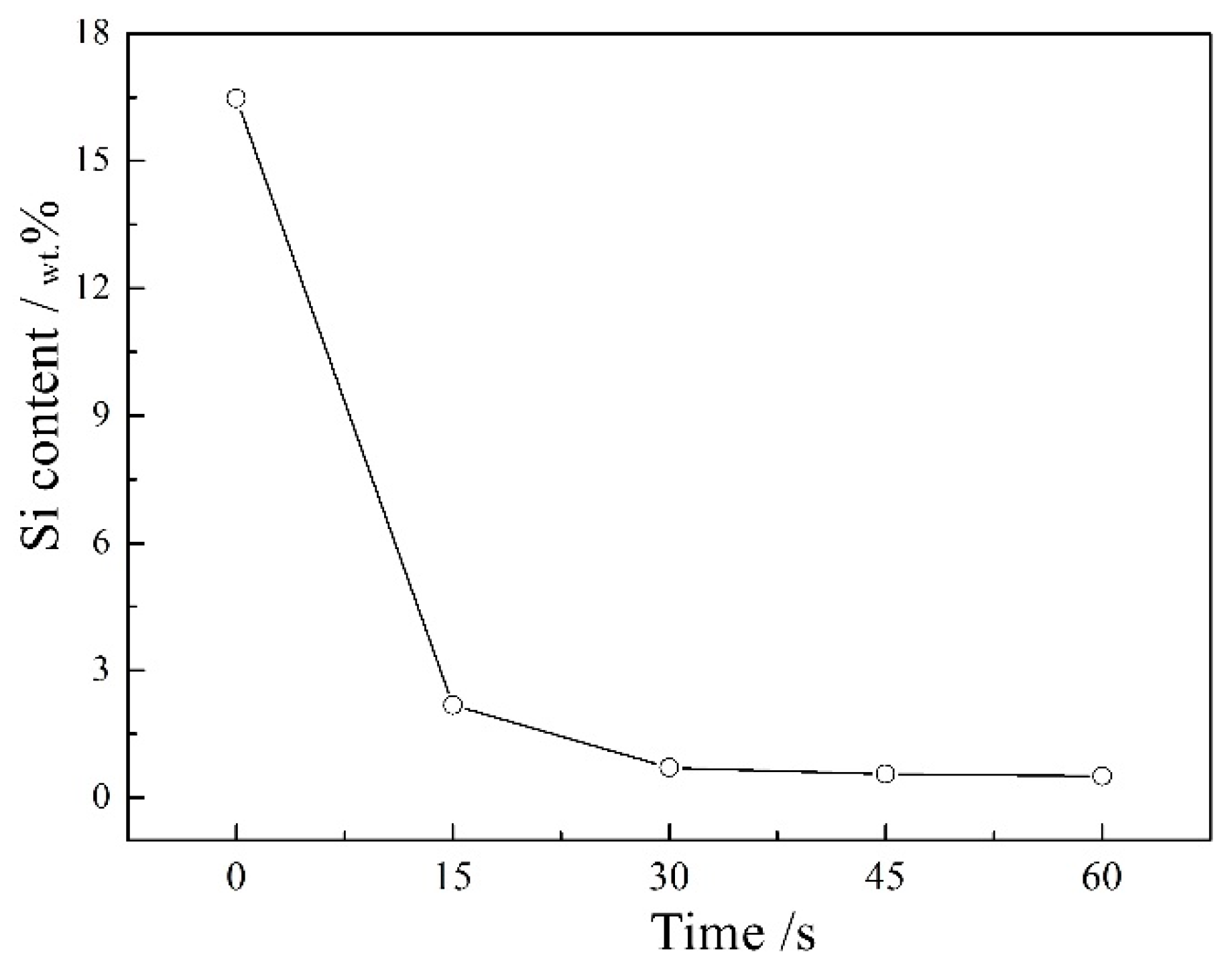
Figure 1. Si content on the surface of Al-12 Si treated by different etching times.
Coatings 11 00453 g001
Figure 2. Surface topography of Al-12 Si after (ad) 0, 15, 30, and 60 s etching treatment.
Coatings 11 00453 g002
Figure 3. Surface roughness of Al-12 Si by different etching treatment time.
Coatings 11 00453 g003
Figure 4. Discharge sparks on the surface of Al-12 Si with (a1d1) 0, 15, 30, and 60 s etching treatment at the 5th min of MAO treatment; (a2d2) 0, 15, 30, and 60 s etching treatment at the 10th min of MAO; (a3d3) 0, 15, 30 and 60 s etching treatment at the 20th min of MAO treatment; (a4d4) 0, 15, 30 and 60 s etching treatment at the 30th min of MAO treatment.
Coatings 11 00453 g004
Figure 5. The thickness increasing of layers on different Al-12 Si during different MAO periods.
Coatings 11 00453 g005
Figure 6. Surface morphology of the coatings on the Al-12 Si by (ad) 0, 15, 30 and, 60 s etching, and then 30 min of MAO treatment.
Coatings 11 00453 g006
Figure 7. Cross-sectional images and EDS composition depth profiles of the coatings on the Al-12 Si by (a,b) 0, (c) 15, (d) 30 and (e,f) 60 s etching, respectively, and then 30 min MAO treatment.
Coatings 11 00453 g007
Figure 8. XRD spectra of layers on Al-12 Si by different etching times after (a) 10, (b) 20, and (c) 30 min. of MAO treatment, respectively.
Coatings 11 00453 g008
Figure 9. Polarization curves and anticorrosion properties of (a) Al-12 Si matrix, (be) Al-12 Si with etching for 0, 15, 30, 60 s, respectively, and then 30 min of MAO treatment.
Coatings 11 00453 g009
Figure 10. Weight loss of (a) Al-12 Si matrix, (be) Al-12 Si with etching for 0, 15, 30, 60 s, respectively, and then 30 min of MAO treatment.
Coatings 11 00453 g010
Figure 11. Surface morphology of (a) Al-9 Si and (b) Al-15 Si with 60 s etching treatment.
Coatings 11 00453 g011
Figure 12. Average growth rate (a) and specific energy consumption (b) of different Al-Si alloys by 10 min. of MAO treatment.
Coatings 11 00453 g012
Figure 13. The morphology of etching pits at different MAO treatment time: (a) 2 min; (b) 5 min; (c) 10 min; (d) 20 min.
Coatings 11 00453 g013
Figure 14. Layer growth model for the Al-Si alloy with etching pretreatment, at the (a) Ⅰ, (b) Ⅱ, (c) Ⅲ, and (d) Ⅳ oxidation stages.
Coatings 11 00453 g014
Table 1. The positive voltage and layer thickness for Al-12 Si by different pretreatment and MAO time.
Etching Time/s0153060
MAO time/min2030203020302030
Positive voltage/V434456466475462470457467
Layer thickness/μm12.714.914.722.815.925.217.125.6
Publisher’s Note: MDPI stays neutral with regard to jurisdictional claims in published maps and institutional affiliations.