
Optical Constant and Conformality Analysis of SiO2 Thin Films Deposited on Linear Array Microstructure Substrate by PECVD


School of Opto-Electronic Engineering, Xi’an Technological University, Xi’an 710021, China
*
Author to whom correspondence should be addressed.
Coatings 2021, 11(5), 510; https://doi.org/10.3390/coatings11050510
Submission received: 14 April 2021
/
Revised: 24 April 2021
/
Accepted: 25 April 2021
/
Published: 26 April 2021
Abstract
:SiO2 thin films are deposited by radio frequency (RF) plasma-enhanced chemical vapor deposition (PECVD) technique using SiH4 and N2O as precursor gases. The stoichiometry of SiO2 thin films is determined by the X-ray photoelectron spectroscopy (XPS), and the optical constant n and k are obtained by using variable angle spectroscopic ellipsometer (VASE) in the spectral range 380–1600 nm. The refractive index and extinction coefficient of the deposited SiO2 thin films at 500 nm are 1.464 and 0.0069, respectively. The deposition rate of SiO2 thin films is controlled by changing the reaction pressure. The effects of deposition rate, film thickness, and microstructure size on the conformality of SiO2 thin films are studied. The conformality of SiO2 thin films increases from 0.68 to 0.91, with the increase of deposition rate of the SiO2 thin film from 20.84 to 41.92 nm/min. The conformality of SiO2 thin films decreases with the increase of film thickness, and the higher the step height, the smaller the conformality of SiO2 thin films.
1. Introduction
SiO2 is a commonly used optical thin film material with low refractive index. SiO2 thin films have many advantages, such as high light transmittance, good insulation, good dielectric properties, and strong corrosion resistance. At present, SiO2 thin films have been widely used in optical film devices, electronic devices, integrated devices, sensors, and other fields [1,2,3,4,5,6]. However, several new applications for SiO2 thin films will require conformal coverage (good conformality) of micro- and nano-scale features in the substrate. Conformality, conformal coverage, or step coverage are important for many applications such as array optical filters, microelectronics [7,8,9], integrated circuit technologies [10,11], and nano-imprint lithography [12,13]. The main methods of preparing SiO2 thin films are physical vapor deposition (PVD), chemical vapor deposition (CVD), Sol-Gel method, and liquid precipitation deposition (LPD) [14,15,16,17]. Generally, when the thin film is deposited on a patterned substrate with CVD technology, it is easy to obtain good conformality, while it is difficult with PVD [18,19].
The conformality or step coverage has been previously reported to depend on deposition parameters, including deposition temperature, total gas flow, and substrate material. Levin et al. studied the relationship between deposition pressure and step coverage of SiO2 thin films prepared by CVD [20]. Gao et al. studied the effects of precursors and substrate materials on step covering in metal organic chemical vapour deposition (MOCVD) [21]. Machida improved the film step covering by adding bias [22]. Bierner et al. studied the effect of the ratio of gaseous reactants on step coverage in the PECVD of silicon nitride [23]. Özkol et al. deposited hydrogenated amorphous silicon (a-Si:H) films by PECVD and studied the relationship between the conformality of a-Si:H films and deposition temperature [24]. However, the effect of deposition rate, especially substrate size characteristics on the conformality of SiO2 thin films, has rarely been addressed. Furthermore, Siriwongrungson, et. al. [25] proposed a quantitative measure of the conformality of the thin film deposit over any shape of feature. Conformality is calculated based on a statistical analysis of a number of film thickness measurements of a fracture surface over the features of interest. However, in this method, film thickness is measured by a field emission scanning electron microscope (FESEM). Moreover, it is required to give the thickness of the film at many points on a fracture surface.
In this work, the new method to quantitatively measure the conformality of thin films on patterned substrate is proposed. The optical properties of silicon dioxide thin films prepared by PECVD were investigated, and the influence of deposition rate and the size of substrate steps on the conformality of the thin films were emphatically analyzed.
2. Analysis Methods
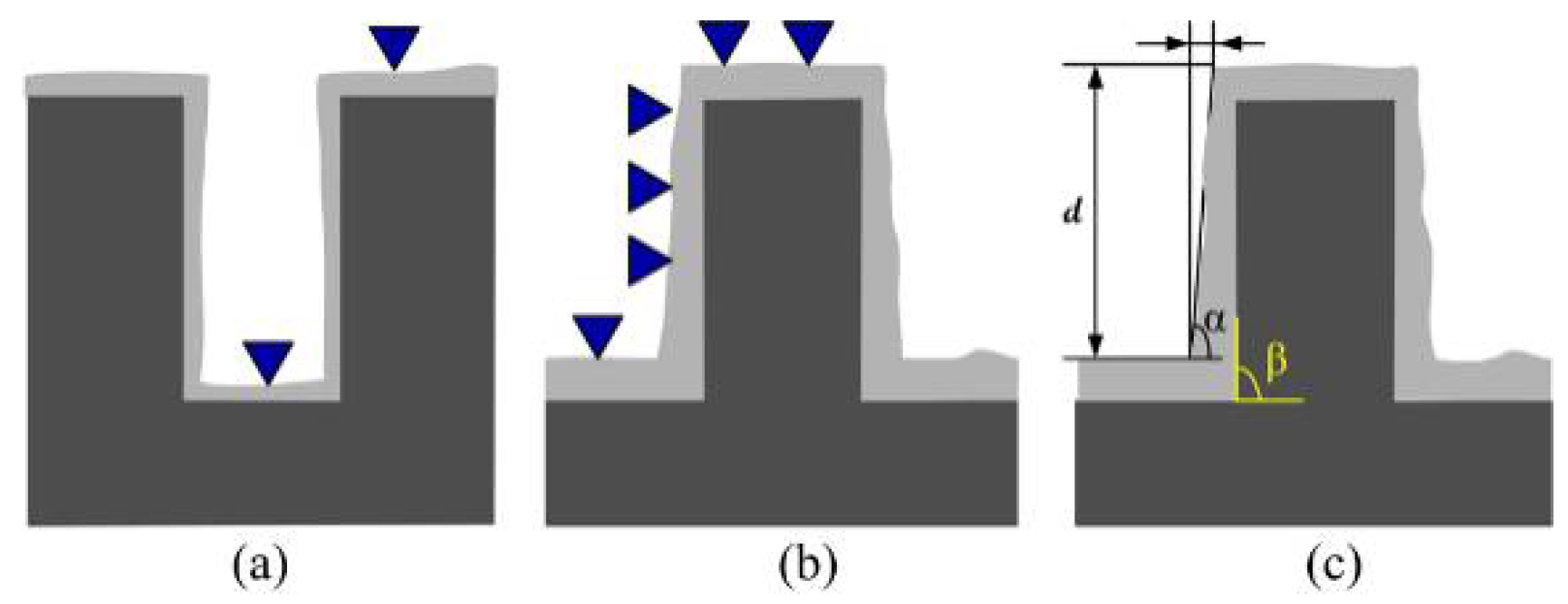
The step coverage is generally defined as the ratio of the film thickness at the trench bottom to the thickness on the flat at the trench mouth opening, as shown in Figure 1a. Krumdieck, et. al. [25,26] proposed a quantitative step coverage assessment method to describe the conformality of a sample in the dimension of interest. This method of measuring conformality is a statistical method, so it requires measuring the thickness of a large number of films at different locations. Conformality is calculated based on a statistical analysis of a number of film thickness measurements of a fracture surface over the features of interest, as shown in Figure 1b. Conformality (C1) can be written as shown in Equation (1) [26].
where M is the number of film thickness measurements, is the film thickness measured at point i, and is the average film thickness calculated from all of the measurements. We propose another method to quantitatively measure the conformality of thin films deposited on the surface of steps, as shown in Figure 1c. Conformality (C2) can be written as
where β is the angle between the bottom edge of the step and the side of the step on the cross section of the basement step before coating and α is the angle between the side and the bottom of the step on the cross section after coating. d and l are can been measured on a cross section using Hitachi SU1510 scanning electron microscope (SEM, Hitachi, Ibaraki, Japan), or can been measured by Surface Profiler (Taylor Hobson, Leicester, UK), .
3. Experimental Details
SiO2 thin films are deposited using PECVD technique, from appropriated gaseous mixtures of silane (SiH4, purity, 99.999%) and nitrous oxide (N2O, purity, 99.99%). The film deposition equipment is a PD-220 PECVD system produced by SAMCO (Kyoto, Japan), as shown in Figure 2 schematically. The reaction system is a parallel planar discharge system. The upper electrode is connected to a 13.56 MHz rf power supply, and the lower electrode supports the substrate and is connected to a 13.56 MHz RF bias power supply. The substrate is arranged on a tray and the heating system under the tray heats the substrate. Before SiO2 thin films deposition, the substrate is bombarded for about 5 min with N2 discharge (discharge pressure: 5 × 10⁻² Pa) of 80 W RF power to improve adhesion between the film and the substrate [27]. The substrate is a single crystal silicon sheet patterned through lithography and etching to obtain step shaped profile. SiO2 thin films are deposited by reaction of silane and nitrous oxide, in which the flow rate of SiH4 is 50 sccm, the flow rate of N2O is 70 sccm, the RF power is 150 W, and the operating temperature is 250 °C. In order to study the effect of the deposition rate of the SiO2 thin film on the conformality, the gas flow ratio SiH4:N2O (50:70), reaction temperature (250 °C), and RF power are kept constant, and the reaction pressure is only changed between 80 and 120 Pa.
The core levels of Si 2p, O 1s, and C 1s are analyzed and the structure of the SiO2 thin films is characterized by X-ray photoelectron spectroscopy (XPS). XPS analysis is performed on a vacuum generators (Fisons Instruments, Loughborough, UK) MT-500 with a non-monochromatic Al X-ray source (Kα 1486.6 keV) and a CLAM-2 hemispherical analyzer for electron detection. The samples are supported on carbon adhesive tape. The refractive index n, extinction coefficient k, and thickness d of SiO2 thin films are characterized using a J.A. Woollam M-2000UI (J.A.Woollam, Lincoln, USA) variable angle spectroscopic ellipsometer (VASE) in the wavelength region between 380 and 1600 nm. The cross-section of SiO2 thin films is observed by a scanning electron microscopy (SEM). Substrate microstructure and SiO2 thin film surface profile are measured by Taylor Hobson TalySurf CCI-2000 (Taylor Hobson, Leicester, UK) surface profilometer.
4. Results and Discussion
The stoichiometry of silicon oxide thin film is determined by the XPS using the Si 2p and O 1s binding energy. Figure 3 shows the XPS spectrum of the silicon oxide thin film deposited at a substrate temperature of 250 °C. The XPS results showed that (Figure 3a) Si 2p has a peak at 103.3 eV and (Figure 3b) O 1s has a peak value at 533.1 eV, indicating that the deposited silicon oxide thin films are SiO2 thin films [28]. In case of stoichiometry SiO2 thin film, the silicon atom surrounded by four oxygen atoms has a characteristic binding energy (103.3 eV).
The optical constants n and k are determined by fitting the ellipsometer parameters in the wavelength region from 380 to 1600 nm. Figure 4 shows the refractive index n and extinction coefficient k of SiO2 thin films deposited at a substrate temperature of 250 °C, discharge power 150 W, and working pressure 100 Pa. As can be seen from Figure 4, both the refractive index and extinction coefficient of SiO2 film change with the wavelength, which indicates that the SiO2 film has a certain dispersion. The refractive index and extinction coefficient of the deposited SiO2 thin films at 500 nm are 1.464 and 0.0069, respectively. The results show that the deposited SiO2 thin films can be used in optical films with low refractive index.
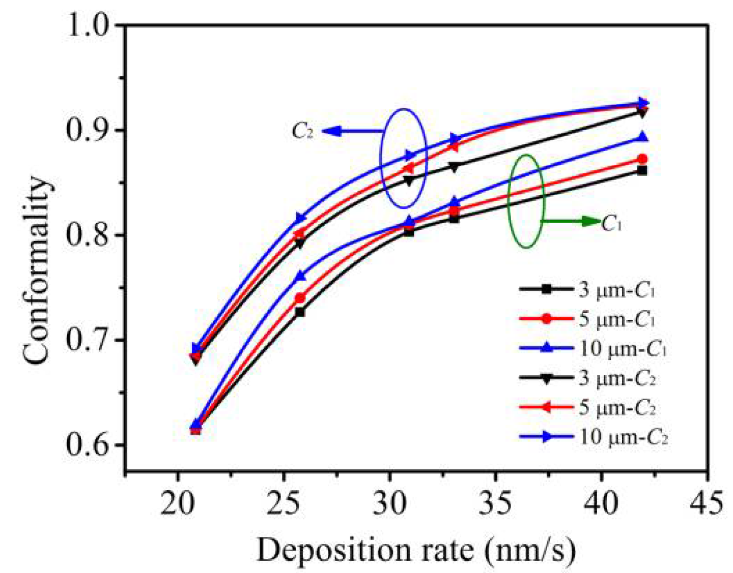
SiO2 thin films are deposited at the flow ratio of 50/70 of SiH4 and N2O; the substrate temperature is 250 °C; the RF discharge power is 150 W; and the reaction pressure is 80, 90, 100, 110, and 120 Pa, respectively. The deposition rates of SiO2 thin films are 20.84, 25.76, 30.91, 33.04, and 41.92 nm/min, respectively. SiO2 thin films of 600 nm thickness are deposited at different deposition rates on linear array micro-structural substrate with a height of 1000 nm and widths of 3, 5, and 10 µm, respectively. The deposition rates of SiO2 thin films are 20.84, 25.76, 30.91, 33.04, and 41.92 nm/min, respectively. Based on this, the effects of deposition rates on the complex properties are studied.
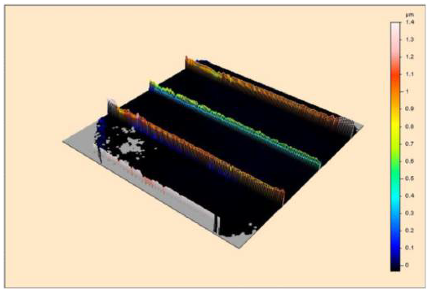
The SEM images are used to estimate the film thickness at the top surface, side walls, and bottom of 15 different positions on the substrate step, and the conformality (C1) is calculated by Equation (1). The surface contour of SiO2 thin films is measured by surface profilometer, and the conformality (C2) is obtained by Equation (2). Figure 5 shows the image measured by surface profilometer of 600 nm SiO2 thin films deposited on an array substrate with a height of 1000 nm and width of 5 µm and deposition rate of 41.92 nm/min. As can be seen from Figure 5, the SiO2 thin films with good conformality can be grown on linear array microstructure substrate at a deposition rate of 41.92 nm/min. Figure 6 shows the conformality results as a function of deposition rate. As can be seen from the Figure 6, under the same conditions, the conformality (C1) calculated by Equation (1) is slightly less than the value of the conformality (C2) calculated by Equation (2). The conformality (C1) and (C2) of the SiO2 thin films deposited on the substrate with a step height of 1000 nm and a step width of 3 μm is approximately 0.86 and 0.89, respectively, when the deposition rate of SiO2 thin film is 41.92 nm/min. Moreover, the conformality of the SiO2 thin films increases with the increase of deposition rate. The conformality of SiO2 thin films is proportional to the deposition rate. As expected, at higher deposition rate, the surface reaction is the rate limiting step which produces conformal coverage of the step shapes.
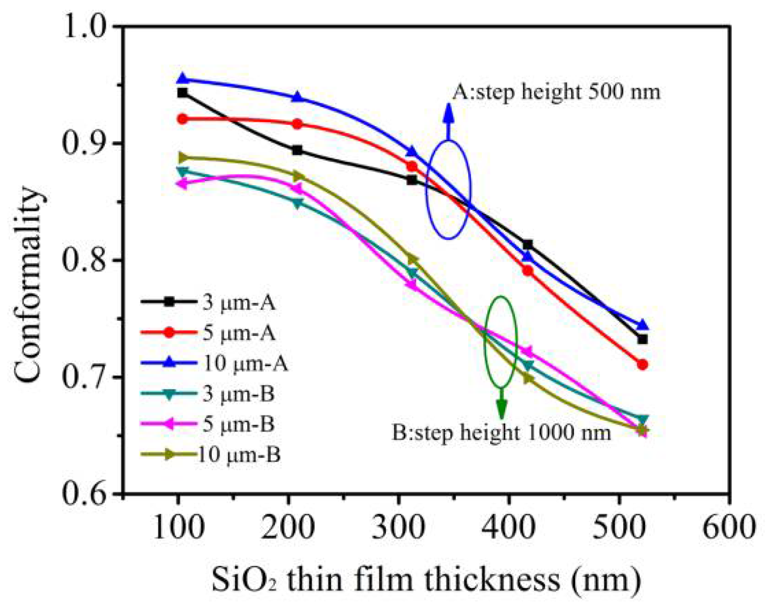
When the deposition rate of SiO2 thin films is 30.91 nm/min, SiO2 thin films of different thicknesses are deposited on 30 substrates of 6 different surface structures with step widths of 3, 5, and 10 µm and step heights of 500 and 1000 nm, respectively. Figure 7 shows the conformality (C2) as a function of SiO2 thin film thickness. In Figure 7, the conformality of all SiO2 thin film samples are calculated by Equation (2). The conformality is inversely dependent on SiO2 thin film thicknesses. Within a certain range, the thinner the film, the better the conformality; the increase of film thickness, the shadow effect, and the inherent characteristics of film growth will make the conformality decrease. Moreover, the conformality of SiO2 thin films on the substrate with a step height of 1000 nm is lower than that on the substrate with a step height of 500 nm. At the same step height, the step width has little effect on the conformality of SiO2 thin films. When the height of the step is 500 nm and the width of the step is 5 µm, the conformality of SiO2 thin films with thickness of 104 nm is 0.92 and that of the SiO2 thin films with thickness of 521 nm is 0.71.
5. Conclusions
A method for quantitative evaluation of the conformality of thin films by measuring the angles of step before and after thin films deposition is proposed. SiO2 thin films are deposited by RF PECVD technique using SiH4 and N2O as precursor gases. The experimental results show that the minimum and maximum deposition rates of SiO2 thin films are 20.84 and 41.92 nm/ min, respectively, when the gas flow of SiH4 and N2O is 50 and 70 sccm, the RF power is 150 W, the reaction temperature is 250 °C, and the gas reaction pressure vary between 80 and 120 Pa. The XPS spectrum indicates that the deposited thin film is SiO2 thin films with a refractive index of about 1.464 at the wavelength of 500 nm.
The results of the film conformality evaluation method proposed in this paper are consistent with the results of the evaluation method given in literature [25], with a slight difference in value. The relation between the deposition rate and the conformality of SiO2 thin films with the same step height and different step widths is obtained. The relationship between the conformality of SiO2 thin films and the film thickness is given under different step size characteristics on the substrate. In general, the conformality of SiO2 thin films prepared by PECVD is proportional to the deposition rate and inversely related to the film thickness.
Author Contributions
Conceptualization, Y.P.; Data curation, J.J. and J.Z.; Investigation, H.L. and Z.W.; Methodology, H.L.; Writing–original draft, Y.P. All authors have read and agreed to the published version of the manuscript.
Funding
The authors acknowledge financial support by the basic research project of natural science of Shaanxi province (2018JM6031). Scientific Research Program Funded by Shaanxi Pro-vincial Education Department (Program No. 18JS054).
Institutional Review Board Statement
Not applicable.
Informed Consent Statement
Not applicable.
Data Availability Statement
The data presented in this study are available on request from the corresponding author.
Conflicts of Interest
The authors declare no conflict of interest.
References
- Nam, T.; Lee, H.; Choi, T.; Seo, S.; Yoon, C.M.; Choi, Y.; Jeong, H.; Lingam, H.K.; Chitturi, V.R.; Korolev, A.; et al. Low-temperature, high-growth-rate ALD of SiO2 using aminodisilane precursor. Appl. Surf. Sci. 2019, 485, 381–390. [Google Scholar] [CrossRef]
- Wang, L.; Jiang, Y.; Jiang, C.; Liu, H.; Ji, Y.; Zhang, F.; Fan, R.; Chen, D. Effect of oxygen flow rate on microstructure properties of SiO2 thin films prepared by ion beam sputtering. J. Non-Cryst. Solids 2018, 482, 203–207. [Google Scholar] [CrossRef]
- Liu, H.; Wang, L.; Jiang, Y.; Li, S.; Liu, D.; Ji, Y.; Zhang, F.; Chen, D. Study on SiO2 thin film modified by post hot isostatic pressing. Vacuum 2018, 148, 258–264. [Google Scholar] [CrossRef]
- Gignac, L.; Parrill, T.; Chandrashekhar, G. Porous SiO2 films analyzed by transmission electron microscopy. Thin Solid Films 1995, 261, 59–63. [Google Scholar] [CrossRef]
- Choi, D.; Kim, B.-K.; Chung, K.-B.; Park, J.-S. Studies on optical, chemical, and electrical properties of rapid SiO2 atomic layer deposition using tris(tert-butoxy)silanol and trimethyl-aluminum. Mater. Res. Bull. 2012, 47, 3004–3007. [Google Scholar] [CrossRef]
- Tabata, A.; Matsuno, N.; Suzuoki, Y.; Mizutani, T. Optical properties and structrue of SiO2 films prepared by ion-beam sputtering. Thin Solid Films 1996, 289, 84–89. [Google Scholar] [CrossRef]
- Lee, W.-J.; Choa, Y.-H. Highly conformal carbon-doped SiCN films by plasma-enhanced chemical vapor deposition with enhanced barrier properties. Thin Solid Films 2018, 657, 32–37. [Google Scholar] [CrossRef]
- Cale, T.S.; Bloomfield, M.O.; Gobbert, M.K. Two deterministic approaches to topography evolution. Surf. Coat. Technol. 2007, 201, 8873–8877. [Google Scholar] [CrossRef]
- Baxamusa, S.H.; Gleason, K.K. Thin polymer films with high step coverage in microtrenches by initiated CVD. Chem. Vap. Depos. 2008, 14, 313–318. [Google Scholar] [CrossRef]
- Lan, J.K.; Wang, Y.-L.; Chao, C.G.; Lo, K.-Y.; Cheng, Y.L. Effect of substrate on the step coverage of plasma-enhanced chemical-vapor deposited tetraethylorthosilicate films. J. Vac. Sci. Technol. B 2003, 21, 1224. [Google Scholar] [CrossRef]
- Schumacher, M.; Baumann, P.K.; Seidel, T. AVD and ALD as two complementary technology solutions for next generation dielectric and conductive thin-film processing. Chem. Vap. Depos. 2006, 12, 99–108. [Google Scholar] [CrossRef]
- Kim, H.; Lee, H.-B.-R.; Maeng, W.-J. Applications of atomic layer deposition to nanofabrication and emerging nanodevices. Thin Solid Films 2009, 517, 2563–2580. [Google Scholar] [CrossRef]
- Alkaisi, M.; Blaikie, R.; McNab, S. Low temperature nanoimprint lithography using silicon nitride molds. Microelectron. Eng. 2001, 57–58, 367–373. [Google Scholar] [CrossRef]
- Wuu, D.; Lo, W.; Chang, L.; Horng, R. Properties of SiO2-like barrier layers on polyethersulfone substrates by low-temperature plasma-enhanced chemical vapor deposition. Thin Solid Films 2004, 468, 105–108. [Google Scholar] [CrossRef]
- Jeong, C.H.; Lee, J.H.; Lim, J.T.; Gil Cho, N.; Moon, C.H.; Yeom, G.Y. Deposition of SiO2 by plasma enhanced chemical vapor deposition as the diffusion barrier to polymer substrates. Jpn. J. Appl. Phys. 2005, 44, 1022–1026. [Google Scholar] [CrossRef] [Green Version]
- Alvisi, M.; De Nunzio, G.; Di Giulio, M.; Ferrara, M.C.; Perrone, M.R.; Protopapa, L.; Vasanelli, L. Deposition of SiO2 films with high laser damage thresholds by ion-assisted electron-beam evaporation. Appl. Opt. 1999, 38, 1237–1243. [Google Scholar] [CrossRef] [PubMed]
- Putkonen, M.; Bosund, M.; Ylivaara, O.M.; Puurunen, R.L.; Kilpi, L.; Ronkainen, H.; Sintonen, S.; Ali, S.; Lipsanen, H.; Liu, X.; et al. Thermal and plasma enhanced atomic layer deposition of SiO2 using commercial silicon precursors. Thin Solid Films 2014, 558, 93–98. [Google Scholar] [CrossRef]
- Blech, I.A.; Plas, H.A.V. Step coverage simulation and measurement in a dc planar magnetron sputtering system. J. Appl. Phys. 1983, 54, 3489–3496. [Google Scholar] [CrossRef]
- Kondo, T.; Sawada, Y.; Akiyama, K.; Funakubo, H.; Kiguchi, T.; Seki, S.; Wang, M.; Uchida, T. Step coverage study of indium-tin-oxide thin films by spray CVD on non-flat substrates at different temperatures. Thin Solid Films 2008, 516, 5864–5867. [Google Scholar] [CrossRef]
- Levin, R.; Evans-Lutterodt, K. The step coverage of CVD SiO2 glass films. Mater. Lett. 1982, 1, 29–32. [Google Scholar] [CrossRef]
- Gao, Y.; He, S.; Alluri, P.; Engelhard, M.; Lea, A.S.; Finder, J.; Melnick, B.; Hance, R.L. Effects of precursors and substrate materials on microstructure, dielectric properties, and step coverage of (Ba, Sr)TiO3 films grown by metalorganic chemical vapor deposition. J. Appl. Phys. 2000, 87, 124–132. [Google Scholar] [CrossRef]
- Machida, K. SiO2 planarization technology with biasing and electron cyclotron resonance plasma deposition for submicron interconnections. J. Vac. Sci. Technol. B 1986, 4, 818. [Google Scholar] [CrossRef]
- Bierner, J.; Jacob, M.; Schönherr, H. Characterization of step coverage change in ultraviolet-transparent plasma enhanced chemical vapor deposition silicon nitride films. J. Vac. Sci. Technol. A 2000, 18, 2843–2846. [Google Scholar] [CrossRef]
- Özkol, E.; Procel, P.; Zhao, Y.; Mazzarella, L.; Medlin, R.; Šutta, P.; Isabella, O.; Zeman, M. Effective passivation of black silicon surfaces via plasma-enhanced chemical vapor deposition grown conformal hydrogenated amorphous silicon layer. Phys. Status Solidi (RRL) Rapid Res. Lett. 2019, 14. [Google Scholar] [CrossRef]
- Siriwongrungson, V.; Krumdieck, S.P.; Alkaisi, M.M. Conformality investigation of titanium dioxide thin films on 3-D micrometer- and nanometer-scale features by pulsed-pressure metal-organic CVD. Chem. Vap. Depos. 2011, 17, 327–336. [Google Scholar] [CrossRef]
- Siriwongrungson, V.; Alkaisi, M.M.; Krumdieck, S.P. Step coverage of thin titania films on patterned silicon substrate by pulsed-pressure MOCVD. Surf. Coat. Technol. 2007, 201, 8944–8949. [Google Scholar] [CrossRef]
- Kim, Y.; Kim, D.; Yoon, D. PECVD SiO2 and SiON films dependant on the rf bias power for low-loss silica waveguide. Thin Solid Films 2005, 475, 271–274. [Google Scholar] [CrossRef]
- Jeong, H.; Cho, J. Fabrication and evaluation of protective SiOx layers using plasma-enhanced chemical vapor deposition. Surf. Coat. Technol. 2017, 330, 71–76. [Google Scholar] [CrossRef]
Figure 1.
Description of the measurement of step coverage and conformality. (a) Step coverage, (b) conformality proposed by S. P. Krumdieck, and (c) conformality proposed in this work.
Figure 1.
Description of the measurement of step coverage and conformality. (a) Step coverage, (b) conformality proposed by S. P. Krumdieck, and (c) conformality proposed in this work.

Figure 2.
A schematic diagram of the RF PECVD equipment.
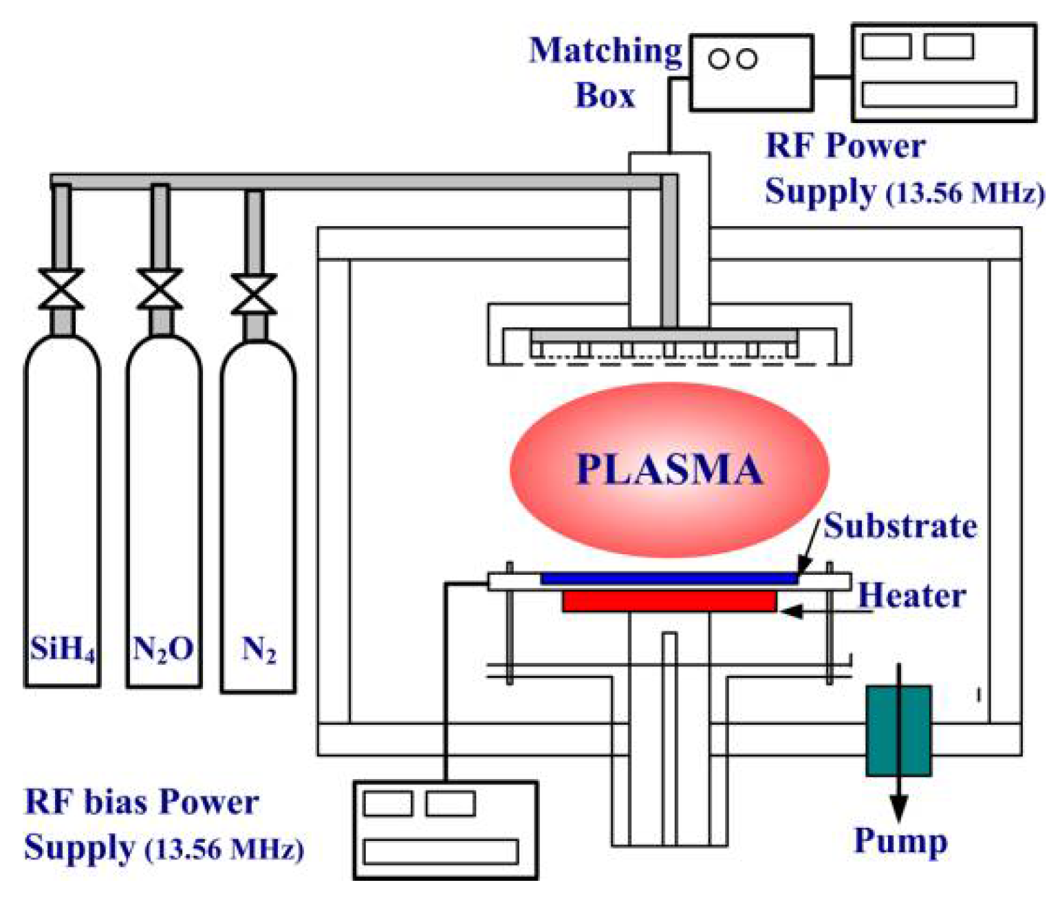
Figure 3.
The XPS spectra of SiO2 thin films deposited by PECVD. (a) Si 2p spectra; (b) O 1s spectra.
Figure 3.
The XPS spectra of SiO2 thin films deposited by PECVD. (a) Si 2p spectra; (b) O 1s spectra.
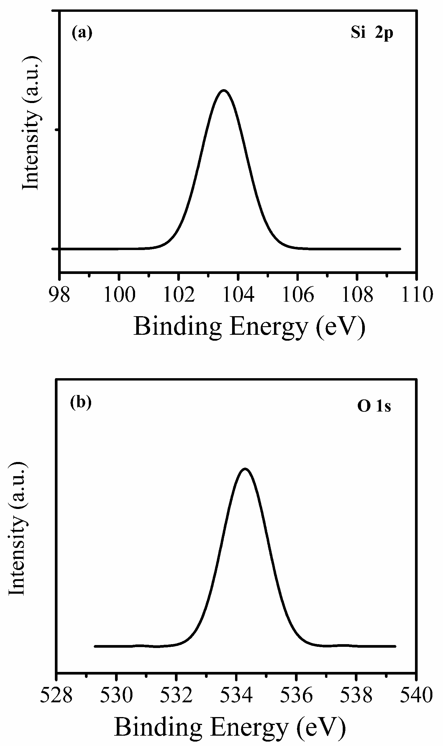
Figure 4.
The refractive index (n) and extinction coefficient (k) of SiO2 thin film as a function of wavelength.
Figure 4.
The refractive index (n) and extinction coefficient (k) of SiO2 thin film as a function of wavelength.

Figure 5.
The images of 600 nm SiO2 thin films deposited on an array substrate measured by surface profilometer.
Figure 5.
The images of 600 nm SiO2 thin films deposited on an array substrate measured by surface profilometer.

Figure 6.
Conformality as functions of the deposition rate.

Figure 7.
Conformality as functions of the SiO2 thin film thickness.
Publisher’s Note: MDPI stays neutral with regard to jurisdictional claims in published maps and institutional affiliations. |
© 2021 by the authors. Licensee MDPI, Basel, Switzerland. This article is an open access article distributed under the terms and conditions of the Creative Commons Attribution (CC BY) license (https://creativecommons.org/licenses/by/4.0/).
Share and Cite
MDPI and ACS Style
Pan, Y.; Liu, H.; Wang, Z.; Jia, J.; Zhao, J. Optical Constant and Conformality Analysis of SiO2 Thin Films Deposited on Linear Array Microstructure Substrate by PECVD. Coatings 2021, 11, 510. https://doi.org/10.3390/coatings11050510
AMA Style
Pan Y, Liu H, Wang Z, Jia J, Zhao J. Optical Constant and Conformality Analysis of SiO2 Thin Films Deposited on Linear Array Microstructure Substrate by PECVD. Coatings. 2021; 11(5):510. https://doi.org/10.3390/coatings11050510
Chicago/Turabian StylePan, Yongqiang, Huan Liu, Zhuoman Wang, Jinmei Jia, and Jijie Zhao. 2021. "Optical Constant and Conformality Analysis of SiO2 Thin Films Deposited on Linear Array Microstructure Substrate by PECVD" Coatings 11, no. 5: 510. https://doi.org/10.3390/coatings11050510
Note that from the first issue of 2016, this journal uses article numbers instead of page numbers. See further details here.