Properties of Hafnium and Aluminium Silicates Coatings Obtained by PLD
by
 , and
, and
Eduard N. Sirjita
, 
Laurentiu Rusen
,
Simona Brajnicov
,
Cristina Craciun
,
Valentin Ion
,
Mihaela Filipescu
* and
Maria Dinescu

National Institute for Lasers, Plasma and Radiation Physics, 409 Atomistilor Street, 077125 Magurele, Romania
*
Author to whom correspondence should be addressed.
Coatings 2021, 11(7), 753; https://doi.org/10.3390/coatings11070753
Submission received: 25 May 2021
/
Revised: 15 June 2021
/
Accepted: 18 June 2021
/
Published: 23 June 2021
(This article belongs to the Collection Pulsed Laser Deposition of Thin Films: Recent Advances and Challenges)
Abstract
:We report on the deposition and characterization of hafnium silicate and aluminium silicate thin films for different applications in optics and electronics. Pulsed laser deposition in a controllable oxygen atmosphere was used as a processing technique, with optimized parameters in terms of laser wavelength, laser fluence and oxygen pressure. The thin films were investigated using atomic force microscopy, spectroscopic ellipsometry, UV–VIS spectroscopy and X-ray photoelectron spectroscopy. The morphological investigations evidenced uniform layers with low roughness (in the order of nanometres). The optical investigations revealed that aluminium silicate layers with low roughness and low absorption in the infrared (IR) range can be obtained at high substrate temperatures (600 °C). The behaviour of the silicate thin films with respect to the nanosecond IR laser irradiation revealed that aluminium silicate layers have higher laser-induced damage threshold values in comparison with hafnium silicate.
1. Introduction
Hafnia and alumina are high-κ dielectrics with remarkable properties, such as high abrasion resistance and high thermal and chemical stability, which make them useful in a wide area of applications: dielectric gate in various types of transistors [1,2], mirrors or antireflective coatings. They can be also used for the development of important components in novel high-temperature energy devices, such as hybrid thermionic converters, as a promising alternative to the presently used ceramics [3]. Besides the aforementioned applications, Al2O3 has also been extensively investigated as a top layer for solar cells [4,5] because it passivates the silicon surface, and it also acts as an electron blocking layer, which increases the built-in potential and reduces recombination [6].
The reflective/antireflective properties of multi-layer dielectric coatings can be tuned by adjusting the thickness of the layers to suit a specific wavelength [7]. Such heterostructures based on Al2O3 and HfO2 have already been studied for mirrors with high laser damage threshold [8]. Furthermore, these materials have also been investigated for high power ultra-short pulse (femtoseconds) laser optics, where the prepulse needs to be transmitted through an optical component, while the main pulse gets reflected [9]. In some applications, SiO2 is also combined with the two oxides in question: in dielectric mirrors, it is the low refractive index material [10,11]; in thin film transistors, it is in the form of a multilayer [12,13]. One of the main requirements for the dielectric gate material is to reduce the operating voltage. This can be done either by reducing the thickness of the dielectric layer, or by using a high-κ material. The drawback of silicon oxide as a dielectric gate is the increase of leakage currents when the film thickness is scaled down [14]. To overcome this, various high-κ dielectric materials were investigated. However, most of these materials have a low crystallization temperature and produce grain boundaries [14]. Moreover, the high-κ dielectric compounds generally have lower optical bandgap energy and smaller energy band offsets compared with the conventional semiconductor oxide (SiO2), decreasing the device’s breakdown voltage.
The development of material mixtures (i.e., silicon oxide and hafnium oxide, or silicon oxide and aluminium oxide) leads to combinations of the positive characteristics of these materials and reduces the unwanted effects, making them suitable as dielectric layers on thin film transistors (TFTs) [15] for applications on silicon devices [16,17].
Hafnium silicate (HfSixOy) layers can be considered an appropriate candidate to be used as active matrix flat panel displays due to their high carrier mobility, optical transparency and electrical stability [18]. Aluminium silicate (AlSixOy) is a refractory compound with good chemical stability that can be used as corrosion and wear-resistant coating for metals and other materials [19].
Usually, thin silicate films are obtained through co-deposition of hafnium oxide or aluminium oxide with silicon oxide using methods such as e-beam evaporation [20], chemical vapor deposition (CVD) [21,22] or pulsed laser deposition (PLD) [23].
In the last decades, the PLD technique has been successfully used to obtain silicates; the research is still scarce compared with other techniques and needs further improvement [23].
The advantage of PLD is that it can yield smooth thin films with controlled stoichiometry and thickness in a reproducible way.
The novelty of this work consists in validation of the PLD technique as a suitable tool to fabricate complex materials such as hafnium and aluminium silicates in the form of thin films that can be used as coatings for laser beam delivery/handling systems. The aim of this study was to prove that these coatings produced using a laser-based technique can resist to high energies generated by pulsed lasers working in the infrared range (IR) of wavelengths and the nanosecond range.
2. Materials and Methods
Thin films of hafnium silicate and aluminium silicate were deposited on quartz plates. The deposition parameters (laser wavelength, laser fluence, oxygen pressure and substrate temperature) were selected based on a laborious parametric study. All layers were obtained as a result of targets irradiation with an ArF excimer laser (wavelength of 193 nm and repetition rate of 20 Hz, 20 ns pulse duration). The targets were sectorial, half a disk of silicon and half a disk of Al2O3 or HfO2. During deposition, the target was continuously rotated and translated. Before the experiment began, the chamber was brought down to a pressure of 10−5 mbar, while during the deposition, the pressure was kept at 10−2 mbar, with a continuous flow of oxygen. In order to evaluate the influence of substrate temperature during the PLD process on the thin film properties, for each combination of materials, two sets of experiments—at room temperature and at 600 °C—have been carried out. The laser fluence value was kept constant for all the experiments (2 J/cm2). The deposition conditions that we varied are presented in Table 1. The number of pulses was chosen in a way to ensure that the coatings have similar thicknesses (around 200 nm). Due to different absorption coefficients of each material at the wavelength of 193 nm, the deposition rate of hafnium oxide is higher than the one of aluminium oxide, and this also contributes to the difference in amounts of silicon in silicates layers that was observed by XPS analyses (Table 2).
The morphological, compositional and optical properties of the thin layers were investigated using atomic force microscopy (AFM), X-ray photoelectron spectroscopy (XPS), spectroscopic ellipsometry (SE) and UV–VIS spectroscopy.
The AFM images were acquired with an XE100 microscope from Park System (Suwon, Korea). Different areas (20 μm × 20 μm and 5 μm × 5 μm) were investigated in order to extract data about the surface roughness (Rq) of the as-deposited silicate thin films and to determine whether defects such as droplets, pores or cracks were present on the films’ surfaces.
The XPS system (Thermo Fisher Scientific, Waltham, MA, USA) has a monochrome Al Kα X-ray source and a silver anode upgrade. The system is provided with an argon cluster ion source for cleaning the analysed surfaces of contaminants and obtaining the depth profile.
The optical investigation was carried out by the SE technique using a Woollam V-Vase spectro-ellipsometer. Ellipsometry is a non-invasive optical technique used to find the optical constants (refractive index n and extinction coefficient k), dielectric function and absorption coefficient (α) [24]. The optical parameters are determined from the change in the polarization state of light due to reflection (or transmission). The VASE32 software was used for fitting of experimental data. The measured values were expressed as (Ψ) and (Δ). These parameters are defined as the ratio of the reflection coefficients of Fresnel, Rp and Rs for polarizations p and s, respectively:
Ellipsometry is a reliable quantitative method; an optical model is required to generate curves of (Ψ) and (Δ), which are compared with those obtained experimentally. As a measure of the quality of this process, MSE (mean square error) is defined as:
where N is the number of pairs (Ψ, Δ), M is the number of variables in the mathematical model chosen to describe the material and σ is the standard deviation of experimental data. Usually, this model is based on the succession of material layers.
The absorption and transmission were investigated with Lambda 25 UV–VIS spectrophotometer (from Perkin Elmer, Waltham, MA, USA). This versatile apparatus is operating in the ultraviolet (UV) and visible (VIS) spectral ranges and its specific characteristics are: wavelength range, 190–1100 nm; bandwidth, 1 nm; wavelength accuracy at D2 peak (656.1 nm), ±0.1 nm; wavelength reproducibility for 10 measurements at 656.1 nm, ± 0.05 nm.
The laser-induced damage threshold (LIDT) tests were made using the S-on-1 method, where the S refers to the number of pulses exposed for each site. The LIDT measurements were carried out according to ISO 21254-1, 2: 2011 “Test methods for laser-induced damage threshold” standard [25]. Samples were exposed to a focused laser beam using a VarispotTM with a focal length of 100 cm, at a given fluence, test sites being arranged in a matrix-like pattern on the whole surface of the sample. The experimental set-up was described elsewhere [26]. Figure 1 shows a schematic of the automated test station with nanosecond pulses for LIDT measurements.
The laser system used in the LIDT setup was a Q-switched, single longitudinal mode Brilliant-B 10 with SLM module from Quantel (Bozeman, MT, USA), 10 Hz repetition rate, operating at 1064 nm wavelength and around 6 ns pulse duration. All the experiments were carried out in air, at ambient temperature 24 °C ± 1 °C and 40%–45% humidity. Before testing, all the samples were cleaned by blow drying with the Green Clean aerosol spray (Green Clean GmbH, Pantaleon, Austria). The samples were fixed on a XY translation stage module, controlled by a dedicated software (home-made version) coupled to a digital signal processor unit.
Temporal and spatial profile measurements of the laser beam were carried out before each test in order to determine the effective pulse duration (teff) [27] and effective area of the laser spot (aeff) [28]. For samples S2, S3, S5, and S6, teff was 6.1 ns, 6 ns, 6.1 ns and 6.2 ns, respectively. The effective spot area for samples S2, S3, S5 and S6 was 4.5 × 10⁻⁴ cm2, 4.7 × 10⁻⁴ cm2, 4.5 × 10⁻⁴ cm2 and 4.4 × 10⁻⁴ cm2, respectively.
Pulse energy was monitored in real time with a J-25MT-10 kHz type pyroelectric detector from Coherent, Inc (Santa Clara, CA, USA). Differential interference contrast (DIC) microscopy was performed on samples after the test was finished in order to qualify every site test as damaged or non-damaged, using an Axio Lab.A1 microscope (Zeiss, New York, NY, USA). This testing method for all samples allowed us to compare them on the same basis, reducing the errors induced by this procedure to close to zero.
3. Results and Discussions
3.1. Morphological Investigations
We investigated the morphological properties of the films using AFM in non-contact mode. One sample from each set was selected to show the topographical images of the 20 µm × 20 µm surfaces. Root mean square (RMS) roughness values were extracted from the topography images.
Both hafnium silicate (Figure 2) and aluminium silicate (Figure 3) thin layers were continuous and showed no cracks or large visible pores and droplets. The Rq values were below 2 nm. The fact that such a low roughness was measured proves that these films can be used for optical coatings, where a slight increase in roughness would alter the spectral properties of the films.
The influence of temperature on the morphology of the films was almost negligible (Figure 2 and Figure 3); however, the aluminium silicate deposited at 600 °C had a slightly higher roughness (Figure 3). The surface of the virgin quartz substrate was also scanned, and it was found that a pattern of parallel lines on the films’ surface was similar to the features of the substrate surface (data not shown). Most probably, these lines resulted from the substrate cutting and polishing process. Even if the thicknesses of the deposited materials were of few hundreds of nanometres (around 200 nm), these features still appeared on the films.
For additional information regarding larger surface areas, SEM investigations at low magnification (2500×) were performed (data not shown). Rare grains (material accumulations) with sizes below 1 micron could be observed. The surfaces of the layers had no pores or micrometric droplets.
3.2. Compositional Investigations
The atomic percentages of elements in the films, obtained by PLD under different conditions of temperature, are presented in Table 2. The coatings obtained by PLD showed no contamination in depth. It can be observed that the substrate temperature (RT or 600℃) during the deposition did not influence the composition, the atomic percentages of the elements in the hafnium silicate layers being almost the same in both samples (S2 and S3). The same was observed in the case of the aluminium silicate layers.
3.3. Investigations of Optical Properties
The optical properties investigations were performed using spectro-ellipsometry and UV–VIS spectroscopy methods.
The ellipsometry investigations were made only on thin films deposited on the Si(100) substrates because of (i) the depolarisation of the SiO2 (quartz) substrate that reaches up to 30%–40% and (ii) the transparency of the quartz substrate, due to which a reflection appears from behind the substrate.
The experimental data were acquired at three different incident angles of the polarized beam (60°, 65° and 70°), in the range of wavelengths of 250–1300 nm, with a step of 2 nm. The optical model used to fit the experimental data was composed of a stack of four different layers: the Si substrate, the native SiO2 layer (thickness of ~3 nm), the mix layer (HfO2–SiO2 and Al2O3–SiO2) and the top rough layer (50% materials and 50% voids in Bruggeman effective medium approximation (EMA) [24]). For all thin films deposited on the Si substrate, a simple Cauchy dispersion formula was used to fit the experimental data and extract the dispersion of refractive index [24]. The layers thickness, the thickness of the top rough layer and Cauchy constants (An and Bn) are presented in Table 3.
The highest value of roughness (~6 nm) was found for the HfSixOy and the lowest for the AlSixOy layers. In the case of the hafnium silicate layer, the refractive index had a higher value than the one expected (average value between refractive indices of HfO2 and SiO2). For a wavelength of 1064 nm, n was close to 2.22 (Figure 4a). Usually, when a lower refractive index material, such as SiO2, is mixed with a higher refractive index material (HfO2), it is expected to result in an intermediate n value (in this case, below 1.85). A possible explanation for this higher value is the formation on hafnium sub-oxide in the PLD process. A similar value of n was reported by A.K. Gerasimova et al. [29], who showed that a higher value of n corresponds to a Hf4O7 phase, and a lower value to pure HfO2. From what they reported, a value of n = 2.22 corresponds to a 3:7 mixture of the HfO2 and Hf4O7 phases.
Two types of fitting were used: Cauchy and effective medium approximation (EMA), based on Al2O3 and SiO2 parametric values taken from the ellipsometry database (Figure 4b). The fit showed the presence of both materials in the AlSixOy thin film at a ratio of 38.6% SiO2 to 61.4% Al2O3.
The refractive index value calculated using EMA (Figure 5) for the wavelength of 1064 nm was 1.634, which was in agreement with the value obtained with Cauchy fitting (n = 1.6301).
It is known that the study of optical properties is very important when thin films are used as coatings for optics. Therefore, transmission and absorption were measured with an UV–VIS spectrophotometer in the wavelength range of 200–1100 nm. The spectra of the hafnium silicate and aluminium silicate thin layers are shown in Figure 6.
It is clear from the spectra that HfSixOy had a lower transmission than AlSixOy, which had transmission, disregarding the influence of the quartz substrate, between 90% and 95%, with the highest transparency in the Near Infrared (NIR) domain. To obtain the absorption coefficient (α), we used Equation (3):
where d is the thickness and T% is the transmission of the sample.
The absorption spectra are presented in Figure 7. The small inconsistencies and abrupt peaks that appeared were due to the spectrophotometer lamps changing for different wavelength ranges.
3.4. Laser Induced Damage Threshold Tests
In LIDT tests, the surface of the thin films is locally heated to the melting point by a laser (nanosecond pulse), and then it is evaporated. The energy of the nanosecond laser pulse will create also a shock wave, which is responsible for micro cracks that appear on the sample, in addition to the large melting layer of the material created by the heat conduction to an area outside the laser spot size. Coating delamination from sample can also be observed in the case of nanosecond laser pulse damage, as previously reported [30,31,32].
The S-on-1 data are shown in Table 4 for the hafnium silicate and aluminium silicate thin films. The measured H0(N) and H50(N) correspond to the threshold energy densities at 0% and 50% damage probability for a variable number of pulses (N), respectively. The effective laser spot diameter was ~0.24 mm, the angle of incidence on the sample 4° ± 1°, with a number of 144 sites per specimen and a distance of 0.8–1 mm between sites. The first observation that could be made is that in the case of hafnium silicate, the threshold for the destruction was lower for the films grown at 600 °C. The threshold energy densities, relative to the number of pulses applied on each site, are shown in Figure 8 and Figure 9.
Extrapolated S-on-1 damage threshold versus number of pulses for 108 pulses was calculated according to the ISO standard. It can be observed in Figure 8 and Figure 9 that there was a distribution of the nanosecond laser damage probability as a function of laser fluence for all the samples.
For HfSixOy samples, thermal effects could be observed in the post-experiment analysis, as well as a cracking and delamination of the film (Figure 10). The LIDT differences between hafnium silicate samples were determined (Figure 8). Different laser-damage morphologies were observed, with dimensions in order of tens of micrometres. Estimated LIDT standard uncertainty values for the HfSixOy films obtained at RT and 600 °C were between 30% (in J/cm2) and 31% (W/cm2) for the sample S2 (RT) and 42% (in J/cm2) and 43% (W/cm2) for the sample S3 (600 °C). Compared with samples obtained by dual ion beam sputtering or reactive low voltage ion plating [33,34], the results were lower, probably due to the samples defect density observed prior to the investigation, which has an important impact on LIDT [35].
In the case of aluminium silicate films, the estimated LIDT standard uncertainty values were between 18% (in J/cm2) and 19% (W/cm2) for S5 and 26% (in J/cm2) and 27% (W/cm2) for S6. Compared with samples obtained by dual ion beam sputtering coatings [36], aluminium silicate films obtained by PLD showed promising results. The obtained values, taking into account the uncertainty, are also comparable with other data from literature [37].
The HfSixOy thin layers have much lower damage threshold than the AlSixOy layers, therefore they are not recommended as a material for laser optical coatings, at least not for nanosecond laser pulse applications.
4. Conclusions
In this study, complex materials, such as hafnium silicate and aluminium silicate, were obtained as thin layers (coatings) by pulsed laser deposition technique in specific conditions.
The morphological and optical investigations revealed that uniform layers based on aluminium silicates with low roughness (below 2 nm) and low absorption in the IR range can be obtained by PLD at high temperatures. These characteristics, together with the high resistance to the nanosecond laser interaction (high LIDT values: H0(N) = 9.03 J/cm2 and H50(N) = 10.32 J/cm2), make aluminium silicate a promising candidate for laser mirror coatings in the IR domain.
Further improvements are necessary, such as increasing the deposited area and keeping low roughness (1 cm × 1 cm), using high quality substrate plates (supports) and increasing densification of the coatings. These improvements can lead to coatings with high LIDT values which eventually can be of interest for ultrashort IR laser optics and can be tested in the ELI-NP Romania laser facility.
In conclusion, we proved the versatility of PLD towards a wide variety of materials, in particular of hafnium silicate and aluminium silicate, processing at nano- and meso-scale.
Author Contributions
Conceptualization, M.F.; Investigation, L.R., S.B., C.C., and V.I.; Writing—original draft, E.N.S.; Writing—review & editing, M.D. All authors have read and agreed to the published version of the manuscript.
Funding
This work was supported by the National Authority for Research and Innovation in the frame of the Nucleus Program and grant of the Ministry of Research and Innovation, CNS-UEFISCDI, project numbers PN-III-P4-ID-PCCF-2016-0033 (GRAPHENEFERRO) within PNCDI III.
Institutional Review Board Statement
Not applicable.
Informed Consent Statement
Not applicable.
Data Availability Statement
Not applicable.
Acknowledgments
The authors are grateful to A. Matei, National Institute for Lasers, Plasma and Radiation Physics, for her support with the XPS investigations.
Conflicts of Interest
The authors declare no conflict of interest.
References
- Yao, R.H.; Zheng, Z.K.; Xiong, M.; Zhang, X.C.; Li, X.Q.; Ning, H.L.; Fang, Z.Q.; Xie, W.G.; Lu, X.B.; Peng, J.B. Low-temperature fabrication of sputtered high-k HfO2 gate dielectric for flexible a-IGZO thin film transistors. Appl. Phys. Lett. 2018, 112, 103503. [Google Scholar] [CrossRef]
- Woo, C.H.; Ahn, C.H.; Kwon, Y.H.; Han, J.H.; Cho, H.K. Transparent and flexible oxide thin-film-transistors using an aluminum oxide gate insulator grown at low temperature by atomic layer deposition. Met. Mater. Int. 2012, 18, 1055–1060. [Google Scholar] [CrossRef]
- Bellucci, A.; Sabbatella, G.; Girolami, M.; Mastellone, M.; Serpente, V.; Mezzi, A.; Kaciulis, S.; Paci, B.; Generosi, A.; Polini, R.; et al. Dielectric Micro- and Sub-Micrometric Spacers for High-Temperature Energy Converters. Energy Technol. 2021, 9, 2000788. [Google Scholar] [CrossRef]
- Glunz, S.W.; Feldmann, F. SiO2 surface passivation layers–a key technology for silicon solar cells. Sol. Energy Mater. Sol. Cells 2018, 185, 260–269. [Google Scholar] [CrossRef]
- Rehman, M.A.; Akhtar, I.; Choi, W.; Akbar, K.; Farooq, A.; Hussain, S.; Shehzad, M.A.; Chun, S.H.; Jung, J.; Seo, Y. Influence of an Al2O3 interlayer in a directly grown graphene-silicon Schottky junction solar cell. Carbon 2018, 132, 157–164. [Google Scholar] [CrossRef]
- Wei, H.Y.; Shi, J.J.; Xu, X.; Xiao, J.Y.; Luo, J.H.; Dong, J.; Lv, S.T.; Zhu, L.F.; Wu, H.J.; Li, D.M.; et al. Enhanced charge collection with ultrathin AlOx electron blocking layer for hole-transporting material-free perovskite solar cell. Phys. Chem. Chem. Phys. 2015, 17, 4937–4944. [Google Scholar] [CrossRef]
- Raut, H.K.; Ganesh, V.A.; Nair, A.S.; Ramakrishna, S. Anti-reflective coatings: A critical, in-depth review. Energy Environ. Sci. 2011, 4, 3779–3804. [Google Scholar] [CrossRef]
- Zhu, M.P.; Xu, N.; Roshanzadeh, B.; Boyd, S.T.P.; Rudolph, W.; Chai, Y.J.; Shao, J.D. Nanolaminate-based design for UV laser mirror coatings. Light Sci. Appl. 2020, 9, 20. [Google Scholar] [CrossRef] [PubMed] [Green Version]
- Filipescu, M.; Palla-Papavlu, A.; Bercea, A.; Rusen, L.; Cernaianu, M.O.; Ion, V.; Dinescu, M. Antireflective coatings with high damage threshold prepared by laser ablation. Appl. Phys. A Mater. Sci. Process. 2019, 125, 815. [Google Scholar] [CrossRef]
- Stolz, C.J.; Thomas, M.D.; Griffin, A.J. BDS thin film damage competition. Laser-Induced Damage in Optical Materials. In Proceedings of the SPIE, Boulder, CO, USA, 2 September 2008; Volume 7132, pp. 71320C-1–71320C-7. [Google Scholar]
- Ďurák, M.; Velpula, P.K.; Kramer, D.; Cupal, J.; Medřík, T.; Hřebíček, J.; Golasowski, J.; Peceli, D.; Kozlová, M.; Rus, B. Laser-induced damage threshold tests of ultrafast multilayer dielectric coatings in various environmental conditions relevant for operation of ELI beamlines laser systems. Opt. Eng. 2016, 56, 011024. [Google Scholar] [CrossRef]
- Kambayashi, H.; Nomura, T.; Ueda, H.; Harada, K.; Morozumi, Y.; Hasebe, K.; Teramoto, A.; Sugawa, S.; Ohmi, T. High Quality SiO2/Al2O3 Gate Stack for GaN Metal–Oxide–Semiconductor Field-Effect Transistor. Jpn. J. Appl. Phys. 2013, 52, 04CF09. [Google Scholar] [CrossRef]
- Zhang, H.; Zhang, Y.; Chen, X.; Li, C.Y.; Ding, X.W. Low-voltage-drive and high output current InGaZnO thin-film transistors with novel SiO2/HfO2/SiO2 structure. Mol. Cryst. Liq. Cryst. 2017, 651, 228–234. [Google Scholar] [CrossRef]
- Houssa, M.; Pantisano, L.; Ragnarsson, L.Å.; Degraeve, R.; Schram, T.; Pourtois, G.; De Gendt, S.; Groeseneken, G.; Heynsab, M.M. Electrical properties of high-κ gate dielectrics: Challenges, current issues, and possible solutions. Mater. Sci. Eng. R Rep. 2006, 51, 37–85. [Google Scholar] [CrossRef]
- Lee, S.; Yun, D.J.; Rhee, S.W.; Yong, K. Atomic layer deposition of hafnium silicate film for high mobility pentacene thin film transistor applications. J. Mater. Chem. 2009, 19, 6857–6864. [Google Scholar] [CrossRef] [Green Version]
- Lee, J.; Kim, J.H.; Kwon, D.W.; Park, E.; Park, T.; Kim, H.W.; Park, B.G. Electrical Characteristics of Metal-Oxide-Semiconductor Capacitor with High-κ/Metal Gate Using Oxygen Scavenging Process. J. Nanosci. Nanotechnol. 2016, 16, 4897–4900. [Google Scholar] [CrossRef] [PubMed]
- Abadias, G.; Chason, E.; Keckes, J.; Sebastiani, M.; Thompson, G.B.; Barthel, E.; Doll, G.L.; Murray, C.E.; Stoessel, C.H.; Martinu, L. Review Article: Stress in thin films and coatings: Current status, challenges, and prospects. J. Vac. Sci. Technol. A 2018, 36, 020801. [Google Scholar] [CrossRef] [Green Version]
- Gao, Y.N.; Xu, Y.L.; Lu, J.G.; Zhang, J.H.; Li, X.F. Solution processable amorphous hafnium silicate dielectrics and their application in oxide thin film transistors. J. Mater. Chem. C 2015, 3, 11497–11504. [Google Scholar] [CrossRef]
- Apblett, A.W.; Cheatham, L.K.; Barron, A.R. Chemical vapour deposition of aluminium silicate thin films. J. Mater. Chem. 1991, 1, 143–144. [Google Scholar] [CrossRef]
- Cosnier, V.; Olivier, M.; Théret, G.; André, B. HfO2–SiO2 interface in PVD coatings. J. Vac. Sci. Technol. A 2001, 19, 2267–2271. [Google Scholar] [CrossRef]
- Hill, D.H.; Bartynski, R.A.; Nguyen, N.V.; Davydov, A.C.; Chandler-Horowitz, D.; Frank, M.M. The relationship between local order, long range order, and sub-band-gap defects in hafnium oxide and hafnium silicate films. J. Appl. Phys. 2008, 103, 093712. [Google Scholar] [CrossRef]
- Kuo, D.H.; Cheung, B.Y.; Wu, R.J. Amorphous aluminum silicate films by metal-organic chemical vapor deposition using aluminum-tri-sec-butoxide and tetraethyl orthosilicate. J. Non-Cryst. Solids 2003, 324, 159–171. [Google Scholar] [CrossRef]
- Filipescu, M.; Scarisoreanu, N.; Craciun, V.; Mitu, B.; Purice, A.; Moldovan, A.; Ion, V.; Toma, O.; Dinescu, M. High-k dielectric oxides obtained by PLD as solution for gates dielectric in MOS devices. Appl. Surf. Sci. 2007, 253, 8184–8191. [Google Scholar] [CrossRef]
- Fujiwara, H. Spectroscopic Ellipsometry: Principles and Applications; John Wiley & Sons Ltd.: Tokyo, Japan, 2007. [Google Scholar]
- International Standard ISO 21254:2011. In Laser and Laser-Related Equipment—Test Methods for Laser-Induced Damage Threshold. ISO21254-1:2011–Part 1: “Definition and General Principles” ISO 21254-2:2011–Part 2: “Threshold, Determination”; ISO 21254-3:2011–Part 3: “Assurance of Laser Power (Energy) Handling, Capabilities”; ISO 21254-4:2011–Part 4: “Inspection, Detection and Measurement“; International Organization for Standardization: Geneva, Switzerland, 2011.
- Stratan, A.; Zorila, A.; Rusen, L.; Simion, S.; Blanaru, C.; Fenic, C.; Neagu, L.; Nemes, G. Automated test station for laser-induced damage threshold measurements according to ISO 21254-1,2,3,4 standards in Laser-Induced Damage in Optical Materials. Proc. SPIE 2012, 8530, 85301Y. [Google Scholar]
- Zorila, A.; Rusen, L.; Stratan, A.; Nemes, G. Measuring the effective pulse duration of nanosecond and femtosecond laser pulses for laser-induced damage experiments. Opt. Eng. 2013, 52, 054203. [Google Scholar] [CrossRef]
- Stratan, A.; Zorila, A.; Rusen, L.; Nemes, G. Measuring effective area of spots from pulsed laser beams. Opt. Eng. 2014, 53, 122513. [Google Scholar] [CrossRef]
- Gerasimova, A.K.; Aliev, V.S.; Kruchinin, V.N.; Badmaeva, I.A.; Voronkovskii, V.A.; Bortnikov, S.G. Optical properties of HfOx (x < 2) films grown by ion beam sputtering-deposition method. Mater. Res. Express 2019, 6, 016423. [Google Scholar]
- Chichkov, B.N.; Momma, C.; Nolte, S.; von Alvensleben, F.; Tünnermann, A. Femtosecond, picosecond and nanosecond laser ablation of solids. Appl. Phys. A 1996, 63, 109–115. [Google Scholar] [CrossRef]
- Hamad, A.H. Effects of Different Laser Pulse Regimes (Nanosecond, Picosecond and Femtosecond) on the Ablation of Materials for Production of Nanoparticles in Liquid Solution. In High Energy and Short Pulse Lasers; Viskup, R., Ed.; IntechOpen: London, UK, 2016; pp. 305–325. [Google Scholar]
- Ristau, D.; Jupé, M.; Starke, K. Laser damage thresholds of optical coatings. Thin Solid Films 2009, 518, 1607–1613. [Google Scholar] [CrossRef]
- Gallais, L.; Mangote, B.; Zerrad, M.; Commandré, M.; Melninkaitis, A.; Mirauskas, J.; Jeskevic, M.; Sirutkaitis, V. Laser-induced damage of hafnia coatings as a function of pulse duration in the femtosecond to nanosecond range. Appl. Opt. 2011, 50, C178–C187. [Google Scholar] [CrossRef] [PubMed]
- Kičas, S.; Batavičiūtė, G.; Juškevičius, K.; Tolenis, T.; Drazdys, R.; Buzelis, R.; Melninkaitis, A. Characterization and application of HfO2-SiO2 mixtures produced by ion-beam sputtering technology. Laser Induc. Damage Opt. Mater. 2013, 8885, 888521. [Google Scholar]
- Field, E.; Bellum, J.; Kletecka, D. How laser damage resistance of HfO2/SiO2 optical coatings is affected by embedded contamination caused by pausing the deposition process. Pacific Rim Laser Damage Opt. Mater. High-Power Lasers 2015, 9532, 95320J. [Google Scholar]
- Guo, K.S.; Wang, Y.Z.; Chen, R.Y.; Zhang, Y.H.; Sytchkova, A.; Zhu, M.P.; Yi, K.; He, H.B.; Shao, J.D. Laser-induced layers peeling of sputtering coatings at 1064 nm wavelength. Sci. Rep. 2021, 11, 3783. [Google Scholar]
- Negres, R.A.; Stolz, C.J.; Thomas, M.D.; Caputo, M. 1064-nm, nanosecond laser mirror thin film damage competition. Laser-Induc. Damage Opt. Mater. 2019, 11173, 111730N. [Google Scholar]
Figure 1.
Automated nanosecond LIDT test station. DDS—real time damage detection system coupled with central DSP unit, PC+DSP—command computer and digital signal processor.
Figure 1.
Automated nanosecond LIDT test station. DDS—real time damage detection system coupled with central DSP unit, PC+DSP—command computer and digital signal processor.

Figure 2.
AFM images of the surface of HfSixOy layers: (a) deposited at RT (Rq = 1.4 nm) and (b) deposited at 600 °C (Rq = 1.4 nm).
Figure 2.
AFM images of the surface of HfSixOy layers: (a) deposited at RT (Rq = 1.4 nm) and (b) deposited at 600 °C (Rq = 1.4 nm).

Figure 3.
AFM images of the surface of AlSixOy layers: (a) deposited at RT (Rq = 1.6 nm) and (b) deposited at 600 °C (Rq = 1.9 nm).
Figure 3.
AFM images of the surface of AlSixOy layers: (a) deposited at RT (Rq = 1.6 nm) and (b) deposited at 600 °C (Rq = 1.9 nm).
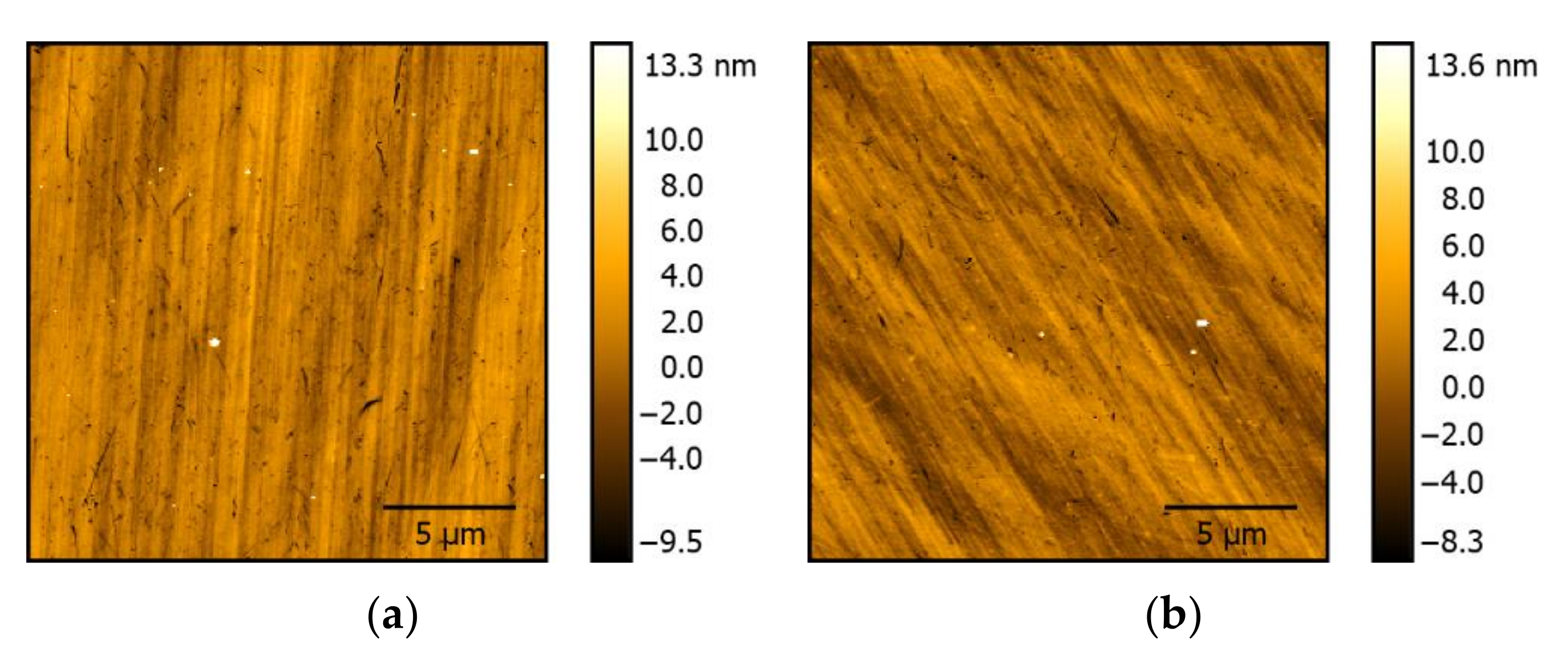
Figure 4.
The dispersion of the refractive index calculated from SE by using Cauchy dispersion formula (a) for hafnium silicate and (b) aluminium silicate layers.
Figure 4.
The dispersion of the refractive index calculated from SE by using Cauchy dispersion formula (a) for hafnium silicate and (b) aluminium silicate layers.

Figure 5.
The dispersion of the refractive index calculated from SE by using EMA in Bruggeman’s model for (a) hafnium silicate and (b) aluminium silicate layers.
Figure 5.
The dispersion of the refractive index calculated from SE by using EMA in Bruggeman’s model for (a) hafnium silicate and (b) aluminium silicate layers.

Figure 6.
Transmission spectra of (a) hafnium silicate and (b) aluminium silicate.

Figure 7.
The absorption spectra of (a) hafnium silicate (b) aluminium silicate.

Figure 8.
Threshold energy densities relative to the number of laser pulses applied per site for hafnium silicate samples. (a) H0(N)—threshold energy density for 0% damage probability and (b) H50(N)—threshold energy density for 50% damage probability.
Figure 8.
Threshold energy densities relative to the number of laser pulses applied per site for hafnium silicate samples. (a) H0(N)—threshold energy density for 0% damage probability and (b) H50(N)—threshold energy density for 50% damage probability.

Figure 9.
Damage probabilities energies densities reported to the number of laser pulses applied per site for aluminium silicate samples: (a) H0(N) and (b) H50(N).
Figure 9.
Damage probabilities energies densities reported to the number of laser pulses applied per site for aluminium silicate samples: (a) H0(N) and (b) H50(N).

Figure 10.
Example of 200× Nomarski micrograph of a damaged site (energy density 3.4 J/cm2, damage after 137 pulses) for sample S2.
Figure 10.
Example of 200× Nomarski micrograph of a damaged site (energy density 3.4 J/cm2, damage after 137 pulses) for sample S2.


Table 1.
Deposition conditions to obtain silicates as thin films by PLD.
| Sample No. | Target | Substrate | No. Pulses | Tsubstrate (°C) |
|---|---|---|---|---|
| S1 | ½ HfO2 + ½ Si | Si (100) | 20,000 | RT |
| S2 | ½ HfO2 + ½ Si | quartz | 144,000 | RT |
| S3 | ½ HfO2 + ½ Si | quartz | 144,000 | 600 |
| S4 | ½ Al2O3 + ½ Si | Si (100) | 40,000 | RT |
| S5 | ½ Al2O3 + ½ Si | quartz | 200,000 | 600 |
| S6 | ½ Al2O3 + ½ Si | quartz | 200,000 | RT |
Table 2.
Composition of silicates layers obtained by PLD at different temperatures.
| Sample No. | O 1s (atomic %) | Al 2p (atomic %) | Si 2p (atomic %) | Hf 4f (atomic %) |
|---|---|---|---|---|
| S2 (HfSixOy at RT) | 64.42 | - | 15.24 | 20.34 |
| S3 (HfSixOy at 600 °C) | 62.55 | - | 14.63 | 22.81 |
| S6 (AlSixOy at RT) | 51.14 | 46.83 | 2.03 | - |
| S5 (AlSixOy at 600 °C) | 57.45 | 40.05 | 2.51 | - |
Table 3.
Thickness and roughness parameters of silicates layers grown on Si(100) plates.
| Sample | An | Bn | Thickness (nm) | Roughness (nm) | MSE |
|---|---|---|---|---|---|
| S1 HfSixOy | 2.203 | 0.015 | 23.3 | 6.4 | 0.6965 |
| S4 AlSixOy | 1.624 | 0.006 | 48.7 | 2.4 | 0.72 |
| EMA (38.6% SiO2 + 61.4% Al2O3) | 49.3 | 1.4 | - | ||
Table 4.
Hafnium silicate and aluminium silicate LIDT test results.
| Sample | Number of Pulses | 1 | 2 | 5 | 10 | 20 | 50 | 100 | 200 | 500 |
|---|---|---|---|---|---|---|---|---|---|---|
| S3 HfSixOy @ 600 °C | H0(N) (J/cm2) | 7.98 | 6.15 | 2.53 | 1.65 | 1.32 | 0.74 | 0.53 | 0.53 | 0.47 |
| H50(N) (J/cm2) | 10.66 | 7.80 | 4.08 | 2.92 | 2.53 | 1.93 | 1.67 | 1.39 | 1.33 | |
| S2 HfSixOy @ RT | H0(N) (J/cm2) | 7.80 | 7.22 | 5.56 | 3.81 | 3.36 | 3.49 | 2.39 | 2.24 | 2.24 |
| H50(N) (J/cm2) | 10.98 | 8.98 | 7.47 | 5.99 | 5.72 | 4.90 | 4.22 | 4.08 | 4.03 | |
| S5 AlSixOy @ 600 °C | H0(N) (J/cm2) | 10.6 | 9.11 | 8.92 | 8.89 | 8.8 | 8.74 | 8.93 | 9.11 | 9.03 |
| H50(N) (J/cm2) | 12.9 | 11.23 | 11.13 | 11.07 | 10.98 | 10.93 | 10.62 | 10.42 | 10.32 | |
| S6 AlSixOy @ RT | H0(N) (J/cm2) | 8.5 | 8.09 | 8.09 | 8.11 | 8.13 | 7.95 | 7.83 | 6.62 | 7.14 |
| H50(N) (J/cm2) | 14.6 | 13.67 | 13.67 | 13.44 | 13.23 | 13.60 | 12.24 | 10.68 | 9.77 |
Publisher’s Note: MDPI stays neutral with regard to jurisdictional claims in published maps and institutional affiliations. |
© 2021 by the authors. Licensee MDPI, Basel, Switzerland. This article is an open access article distributed under the terms and conditions of the Creative Commons Attribution (CC BY) license (https://creativecommons.org/licenses/by/4.0/).
Share and Cite
MDPI and ACS Style
Sirjita, E.N.; Rusen, L.; Brajnicov, S.; Craciun, C.; Ion, V.; Filipescu, M.; Dinescu, M. Properties of Hafnium and Aluminium Silicates Coatings Obtained by PLD. Coatings 2021, 11, 753. https://doi.org/10.3390/coatings11070753
AMA Style
Sirjita EN, Rusen L, Brajnicov S, Craciun C, Ion V, Filipescu M, Dinescu M. Properties of Hafnium and Aluminium Silicates Coatings Obtained by PLD. Coatings. 2021; 11(7):753. https://doi.org/10.3390/coatings11070753
Chicago/Turabian StyleSirjita, Eduard N., Laurentiu Rusen, Simona Brajnicov, Cristina Craciun, Valentin Ion, Mihaela Filipescu, and Maria Dinescu. 2021. "Properties of Hafnium and Aluminium Silicates Coatings Obtained by PLD" Coatings 11, no. 7: 753. https://doi.org/10.3390/coatings11070753
Note that from the first issue of 2016, this journal uses article numbers instead of page numbers. See further details here.