Article

Microstructure and Surface Topography Study of Nanolayered TiAlN/CrN Hard Coating

1
Jožef Stefan Institute, Jamova Cesta 39, 1000 Ljubljana, Slovenia
2
Interkorn d.o.o, Gančani 94, 9231 Beltinci, Slovenia
3
Faculty of Mechanical Engineering, University of Maribor, Smetanova 17, 2000 Maribor, Slovenia
4
Graz Centre for Electron Microscopy, Steyrergasse 17, A-8010 Graz, Austria
*
Author to whom correspondence should be addressed.
Coatings 2022, 12(11), 1725; https://doi.org/10.3390/coatings12111725
Submission received: 12 October 2022 / Revised: 3 November 2022 / Accepted: 8 November 2022 / Published: 11 November 2022
(This article belongs to the Special Issue Surface Topography Effects on Functional Properties of PVD Coatings)

Abstract

:
The microstructure and surface topography of PVD hard coatings are among the most important properties, as they significantly determine their mechanical, tribological and other properties. In this study, we systematically analyzed the microstructure and topography of a TiAlN/CrN nanolayer coating (NL-TiAlN/CrN), not only because such coatings possess better mechanical and tribological properties than TiAlN and CrN monolayer coatings, mainly because the contours of the individual layers, in the cross-sectional STEM or SEM images of such coatings, make it easier to follow topographic and microstructural changes that occurred during its growth. We investigated the effects of the substrate rotation modes on the microstructure and surface topography of the NL-TiAlN/CrN coating, as well as on the periodicity of the nanolayer structure. The influence of the substrate material and the ion etching methods were also studied, while special attention was given to the interlayer roughness and influence of non-metallic inclusions in the steel substrates on the growth of the coating. The topographical features of the NL-TiAlN/CrN coating surface are correlated with the observations from the cross-sectional TEM and FIB analysis. Selected non-metallic inclusions, covered by the NL-TiAlN/CrN coating, were prepared for SEM and STEM analyses by the focused ion beam. The same inclusions were analyzed prior to and after deposition. We found that substrate rotation modes substantially influence the microstructure, surface topography and periodicity of the NL-TiAlN/CrN layer. Non-metallic inclusions in the substrates cause the formation of shallow craters or protrusions, depending on their net removal rates during the substrate pretreatment (polishing and ion etching), as compared to the matrix.

1. Introduction

In order to provide efficient wear protection for tools with PVD hard coatings, besides high hardness, fracture toughness and oxidation resistance, they must have a smooth surface as well. The surface topography of PVD hard coatings is of key importance, especially for their tribological properties [1,2,3,4,5,6]. In the case of the cutting process, for example, a smooth, hard coating surface reduces mechanical interaction with the chip; therefore, the friction and material transfer are also reduced.
  • In our previous works, we discussed, in more detail, the coating surface topography [6,7,8,9]. We have shown that the topography of a PVD coating surface originates from:A substrate surface topography formed during the substrate mechanical pretreatment (grinding, blasting and polishing) and during the substrate cleaning by ion etching prior to the coating deposition;
  • Intrinsic coating features such as grain size, phase composition, texture, etc.;
  • Growth defects (e.g., nodulus and pinholes) formed during the coating growth process.
We have also shown that the multilayered coatings are more suitable for the study of growth defects because the contours of individual layers in the cross-sectional SEM and TEM images reveal their internal structure. That is also the reason why, in this study, we analyzed the surface topography of the TiAlN/CrN nanolayer coating (NL-TiAlN/CrN) in more detail.
On a macroscale, the surface roughness mainly originates from growth defects in a size range above 3 µm. The inspection of the coating surface at lower magnification shows a large number of unevenly distributed growth defects of various shapes and sizes. The growth defect density depends on the type of ion etching and deposition processes and deposition parameters, as well as on the type of substrate material and its mechanical and ion etching pretreatments. In order to change the micro-topography and to reduce the surface roughness of the coated tool, post-coating treatments (polishing and blasting) are often used.
On the microscale, the surface roughness mainly depends on the columnar microstructure and the crystallinity of the coating. Depending on the deposition conditions, the coating microstructure can be coarse columnar, fine columnar or amorphous. The formation of the columnar microstructure on a rough substrate surface is a result of the geometrical shadowing effect. Because the sputtered atoms travel from the source to the substrate in a straight line, the substrate surface morphology affects their angle of incidence; therefore, the surface coverage decreases. However, the growth of columns depends not only on the substrate surface roughness but also on the angle of incidence of the arriving atoms, the deposition temperature and the intensity of energetic particle bombardment [8]. While the first two mechanisms increase the roughness of the coating surface, the other two increase the surface mobility of the depositing atoms, which consequently decreases its roughness or even disrupts the columnar microstructure. A columnar microstructure can also develop on a smooth substrate surface but only if the pronounced preferential growth of crystal planes occurs. The coating surface morphology and, thus, its roughness are determined by the diameter of the columns and by the faceted column tops. Both contributions increase with the coating thickness. Columnar growth can also be observed in the multilayered hard coatings. In such coatings, the growth of some columnar grains stops at the layer interfaces, while others start growing, as the layer interfaces provide more opportunities for the nucleation of new crystal grains. These processes result in a refinement of crystal grains.
During the coating deposition, the surface roughness is increased not only due to columnar growth but also because crystal grains with different orientations grow faster than others. Thus, the growth of new columns with more preferred growth orientations or phases dominates [10]. In a multilayer structure, the last deposited layer can provide a template for the growth of the next layer. If the two materials in the multilayer structure have the same crystal structure and if their lattice mismatch is small enough (no more than several percent), this can result in epitaxial growth [11,12,13]. Epitaxial growth can extend through the whole layer if its thickness is kept small enough (a few nm) [10].
In this paper, we focus on the microstructure, surface topography, interlayer roughness and formation of growth defects in a NL-TiAlN/CrN hard coating. This coating was chosen because the growth defect formation and other coating surface irregularities are easier to observe in a multilayer structure. In addition, the NL-TiAlN/CrN coating possesses enhanced mechanical and tribological properties as compared to TiAlN and CrN monolayer coatings. The stresses formed at the interfaces due to different lattice constants significantly contribute to higher hardness of the nanolayer structure coating in comparison with the corresponding monolayers [14]. The improvement of the coating properties is contributed to the layer interfaces in such a structure, which act as a barrier to dislocation motion, crack propagation and elemental diffusion. In the literature, the NL-TiAlN/CrN coating has been investigated by several groups [13,15,16,17,18]. It was demonstrated that such a coating could be deposited with clear superlattice characteristics. We should also mention that the properties (e.g., morphology, microhardness, fracture toughness and residual stresses) of such nanolayer coatings could be tailored in a controlled manner by varying their modulation period [19].

2. Materials and Methods

The NL-TiAlN/CrN coatings were prepared in the industrial deposition system CC800/9 (Cemecon, Würselen, Germany). The deposition system was, in detail, described elsewhere [8]. The unit was equipped with four unbalanced magnetron sources placed in the corners of a rectangular vacuum chamber. For the deposition of the NL-TiAlN/CrN coatings, two segmental TiAl targets were positioned at one side of the chamber and two Cr targets at the opposite side. The dimension of the sources was 500 mm × 88 mm. The TiAl target was made of a titanium base with 48 cylindrical aluminum plugs within the racetrack. The coating composition was Ti 23 at.%, Al 27 at.%, and N 50 at.%N. In order to form a nanolayer structure, the substrates were mounted on a planetary substrate holder system that enabled up to three-fold rotation. A detailed description of the rotation geometry is given in [20,21]. During the preparation of nanolayer coatings, all the cathodes were operated simultaneously, while the nanolayer structure resulted from the substrate rotation.
As substrates, we used test plates made of cold work tool steel (AISI D2, Ravne steel factory, Ravne, Slovenia), conventional high-speed steel (HSS, AISI M2, Ravne steel factory, Ravne, Slovenia), powder metallurgical tool steel ASP30 (AISI M3:2+Co, Uddeholm, Hagfos, Sweden),stainless steel (AISI 316L, Acroni, Jesenice, Slovenia) and cemented carbide (WC-Co, Mecut, Ceranesi, Italy). Substrates were first ground and polished to a mirror finish, corresponding to surface roughness Sa values of around 12 nm. Before deposition, they were cleaned with detergents and ultrasound, rinsed in deionized water and dried in hot air.
The coating preparation was performed in a standard way, which included substrate heating by resistive heaters up to about 450 °C, etching by argon and krypton ions and DC sputter deposition. In a separate batch, one set of the substrates was cleaned by mid-frequency (MF) ion etching (240 kHz, duty cycle 1600 ns) conducted for 60 min with a peak power of 1400 W. The MF ion etching was performed in mixed argon (flow rate 180 mL/min) and krypton (flow rate 50 mL/min) atmosphere under the pressure of 0.35 Pa, while the bias voltage applied on the turntable was 650 V. The next set of substrates was cleaned by MF ion etching and, additionally, with the so-called “booster” ion etching. During the booster etching, the working gas was injected through the upper and lower booster etch nozzles (i.e., a hollow cathode), where intensive ionization of the working gas (Ar, Kr) occurs. Such additional discharge enhances the plasma density and, thus, the intensity of the etching process.
After ion etching, the sample surfaces were examined with a scanning electron microscope (SEM), energy-dispersive X-ray spectroscopy analysis (EDX), atomic force microscope (AFM) and 3D stylus profilometer. After that, all the substrates were put again into the deposition system where they were once more heated to ~450 °C and cleaned by MF ion etching for just 10 min to remove any possible impurities formed during the previous analysis.
The NL-TiAlN/CrN coating was deposited in a mixture of argon (flow rate 150 mL/min), krypton (flow rate 100 mL/min) and nitrogen (flow rate 70 mL/min) at a total pressure of 620 mPa. A DC bias of −90 V was applied to the substrates. The power on the Cr and TiAl targets was 4.5 kW and 9.5 kW, respectively. Coating thickness was measured by the ball crater method (Calotest), as well as from the SEM images of the sample fracture. For one-, two- and three-fold rotations, the thicknesses were approximately 13.5 µm, 7.5 µm and 3 µm, respectively.
Surface topography of precoated and coated substrates was analyzed by the atomic force microscope Solver PRO (AFM, NT-MDT Spectrum Instruments, Moscow, Russia) and by the 3D stylus profilometer (Bruker Dektak XT, Billerica, MA, USA). The scanning area of AFM was 5 µm × 5 µm. The evaluation area of the 3D stylus profilometer was 1 mm2, while the resolution in x, y and z (vertical) directions were 0.2 μm, 1 μm and around 5 nm, respectively.
The morphology and layer structure of the coatings were studied using Zeiss Supra 35 VP (Jena, Germany), JEOL JSM 6500F and Sirion 400 NC (FEI, Eindhoven, Netherlands) scanning electron microscopes. All three microscopes were field emission SEM with the ability of EDX analysis (Oxford INCA 350, Oxford Instruments, Abingdon, UK). Cross-sections for SEM investigations were also prepared by focused ion beam techniques using an FIB source (Keithley Instruments Inc., Solon, Ohio) integrated into the scanning electron microscope Helios NanoLab NL650 (FEI, Eindhoven, Netherlands).
Detailed microstructural analysis of NL-TiAlN/CrN coating was performed by Jeol JEM-2100 transmission electron microscope (TEM) and a probe corrected Titan 60-300 (Thermo-Fisher, Eindhoven, Netherland) scanning transmission electron microscope (STEM) equipped with a high-angle annular dark-field detector and EDX analysis (ChemiStem set-up, Thermo Fisher, FEI, Eindhoven, Netherlands). It was used to study the interface characteristics at the atomic scale. Some specimens for TEM cross-sectional analysis were prepared by the conventional technique [12], while those for STEM were prepared by using a focused ion beam (FIB) workstation (FEI NOVA 200 Nanolab field emission scanning electron microscope, FEI, Eindhoven, The Netherlands). Four different modes were used to obtain different information of layer interfaces: high-resolution (HRTEM), high-angle annular dark-field (HAADF-STEM) [22], dark-field (DF-STEM) and bright-field (BF-STEM).

3. Results

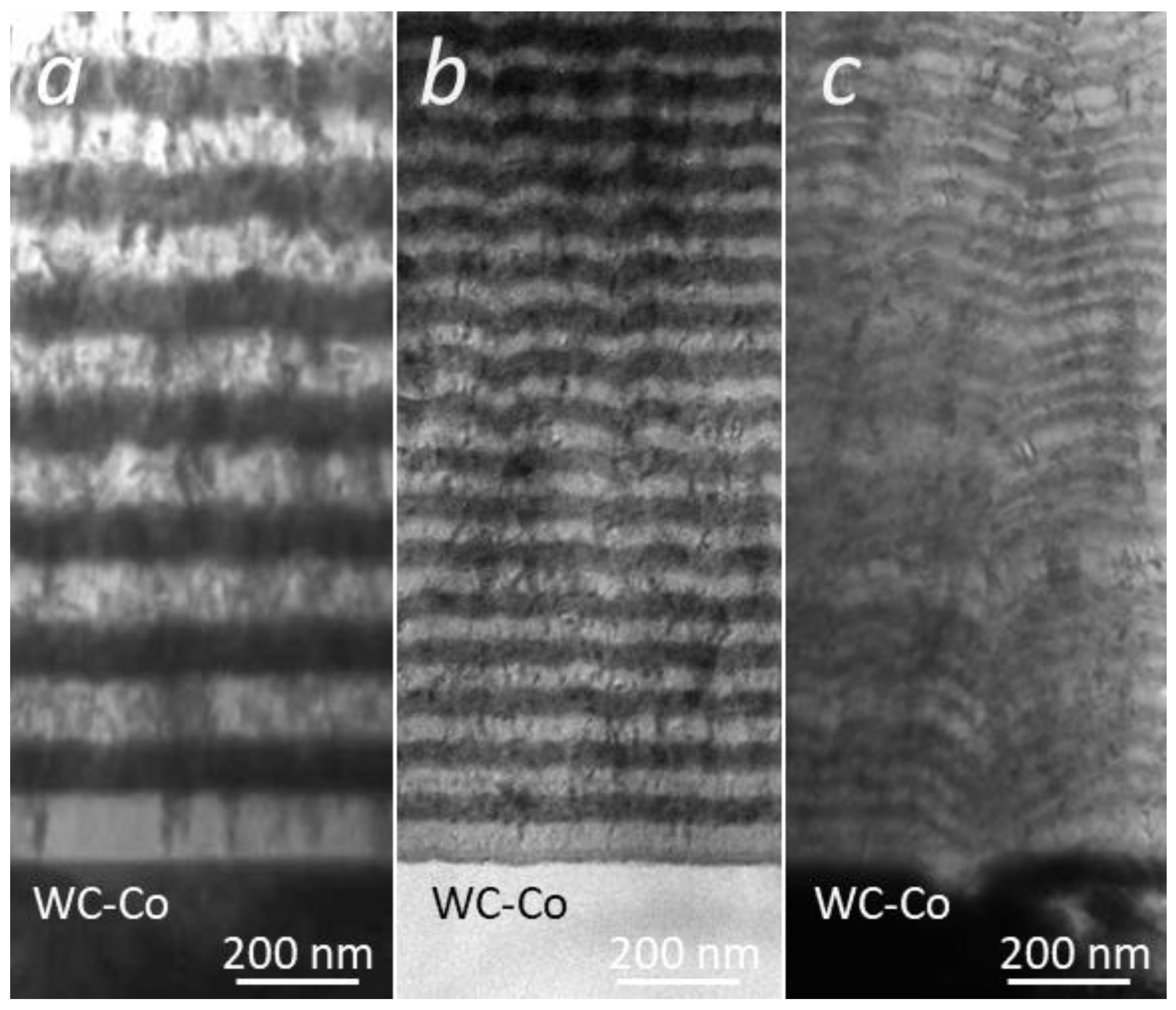
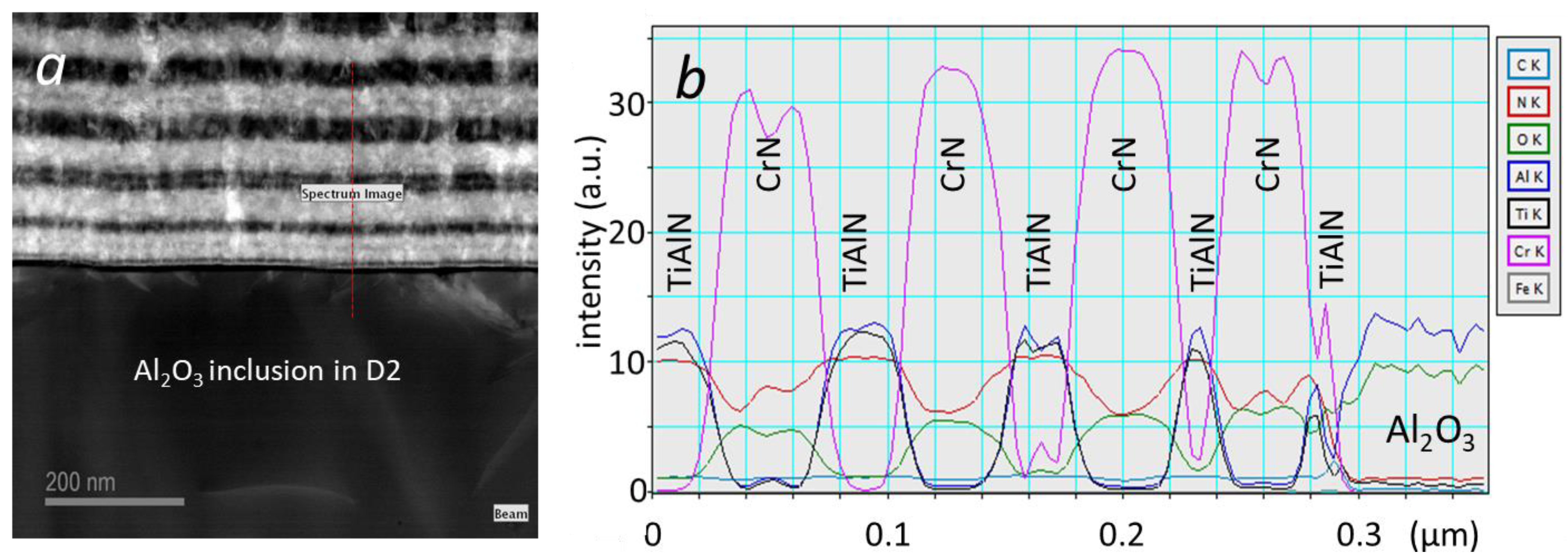
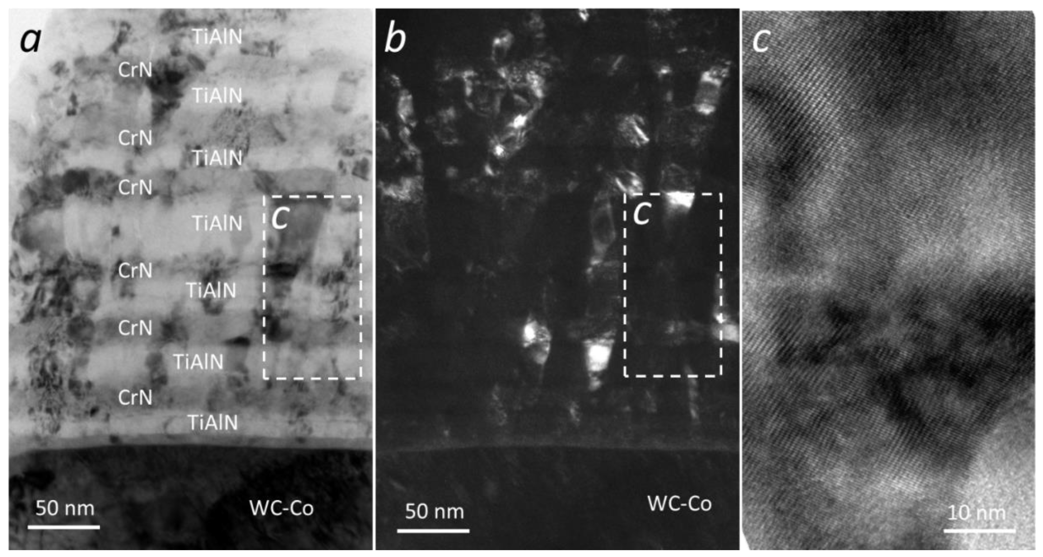
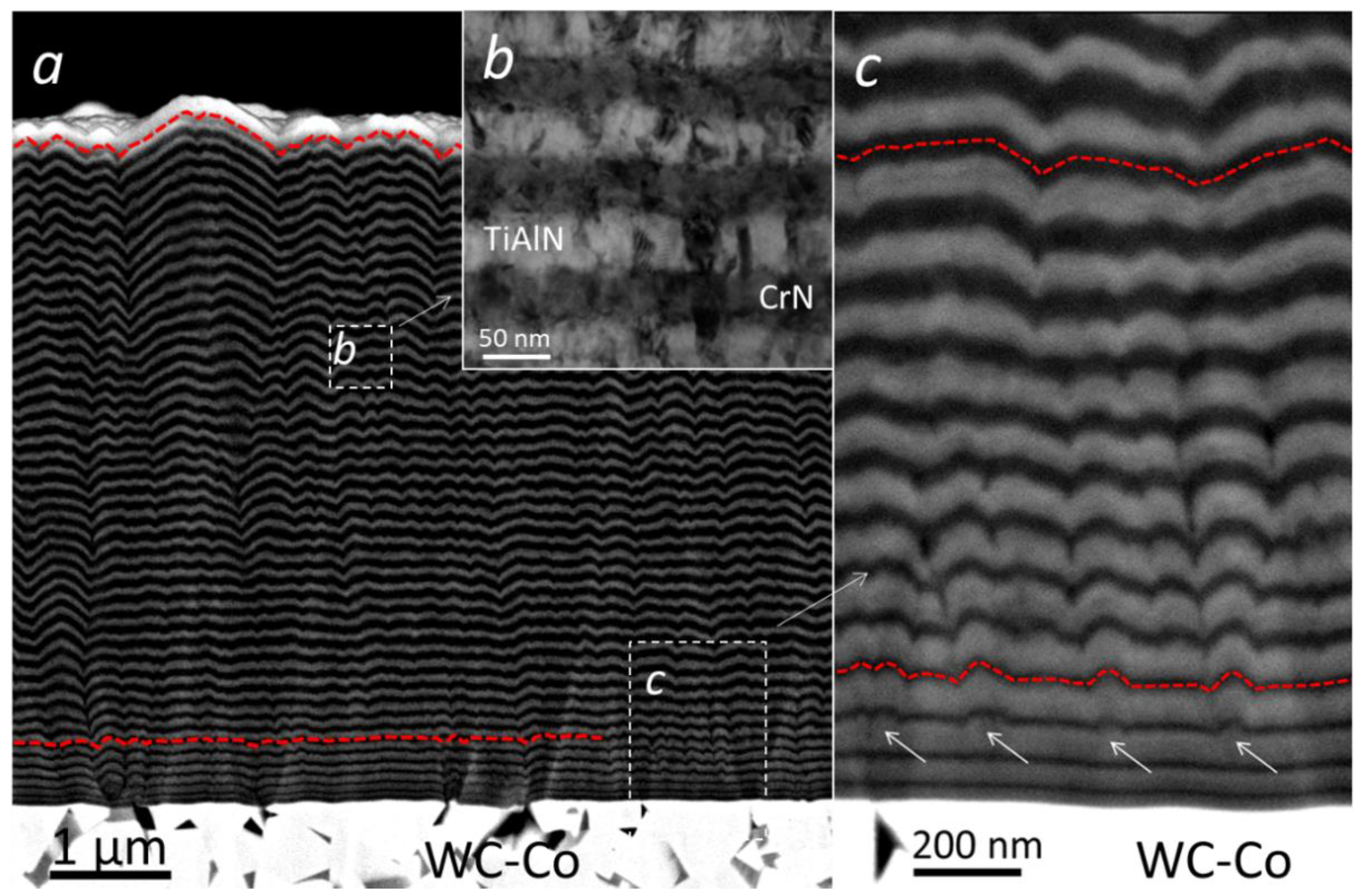
3.1. Microstructure Characterization and Periodicity Analysis

Figure 1 shows the SEM images of the fractured surface of the NL-TiAlN/CrN hard coatings prepared in the same batch by one-, two- and three-fold rotation. The bright layers correspond to TiAlN and the dark ones to CrN. The coatings prepared by single, double and triple rotation differ not only in the total thickness but also in the microstructure and periodicity of the thin layers. All these differences can be better seen in cross-sectional TEM images. Figure 2 shows bright-field (BF) TEM images of the NL-TiAlN/CrN coating taken close to the substrate surface. For samples prepared using the one-fold substrate rotation, the individual layers had similar thicknesses (approximately 90 nm). For samples prepared using the two-fold substrate rotation, the thickness of the individual layers is reduced by about half, in comparison with the one-fold rotation, and varies slightly in coating thickness. In the case of the sample prepared by the three-fold rotation, the layer thickness is between 10 nm and 25 nm.
In our previous articles, we showed that the periodicity of NL-TiAlN/CrN coatings strongly depends on the substrate rotation mode [20,21]. This topic has also been addressed by other authors [23]. In the case of the simplest one-fold rotation, the trajectory of the substrate is a circle. Therefore, the deposition rate and the layer structure are periodic. In the case of the two-fold rotation, the trajectory of the sample is more complex. The number of rotations required to return the sample to the same position and orientation depends on the gear ratio of the planetary substrate holder system. As a result, the layered structure is not fully periodic. This is clearly visible from the STEM image and corresponding EDX analysis (Figure 3). The EDX line scan performed continuously from the aluminum oxide inclusion in the D2 tool steel substrate through the first ten layers shows the relative changes in the content of each element that composes the NL-TiAlN/CrN coating. We should also note that the thickness of the first few layers changes due to an increasing cathode power at the beginning of the deposition. It can be also observed that all interfaces are well defined, without visible intermixing. The addition of a third rotation (in our case non-continuous) results in the formation of still more complex multilayer structures. In this case, the sample practically never returns to the same position and orientation, while the periodicity of the multilayer structure even depends on the initial position of the substrates. Therefore, the layer structure prepared by the three-fold rotation is aperiodic.
It can be also seen that the microstructure of the NL-TiAlN/CrN coating is considerably different for the samples prepared by different rotation modes. The TEM bright-field image reveals polycrystalline elongated columns, perpendicular to the substrate surface. The average width of columns with a curved top surface is around 600 nm, 280 nm and 110 nm, for one-fold, two-fold and three-fold rotation, respectively. In the case of a one-fold rotation, unlike in a two-fold and three-fold rotation, a lot of columnar grains extend from the substrate to the coating surface. The microstructure of the coatings prepared by the two-fold rotation is denser than that prepared by the one-fold rotation. The most fine-grained and compact are the coatings prepared by the three-fold rotation. Although the plasma conditions are identical for the different rotation modes, the trajectories and, particularly, the orientation of the substrate during rotation are very different. In the one-fold rotation, the substrates pass individual magnetron sources following the same trajectory (i.e., the distance and orientation changes are the same in every rotational cycle). However, this is not the case with two-fold and three-fold rotations. The substrate distance and orientation from the center of the turntable and from individual magnetron sources change significantly during the rotation. In certain positions, the sample may still be in the plasma but may face away from the target. In such a position, the coating surface is still exposed to the ion bombardment, while the coating does not grow. Additionally, the incidence angle of ions and the atom flux change constantly during the deposition. It is understandable that such inhomogeneous growth conditions strongly influence the microstructure and surface topography of the coating.
The NL-TiAlN/CrN coating is isostructural as it is composed of TiAlN and CrN individual layers that have the same (fcc—face-centered cubic) crystal structure. Because the lattice mismatch of both fcc crystal structures is small (<2%), epitaxial growth occurred, as can be seen in the high-resolution TEM image (Figure 4). We can see that the lattice fringes are continuous across neighbouring layers, which proves the layer coherency within the columnar grain (Figure 4c). The phenomenon of epitaxial growth in the NL-TiAlN/CrN layer was already discussed in more detail in our previous paper [12].

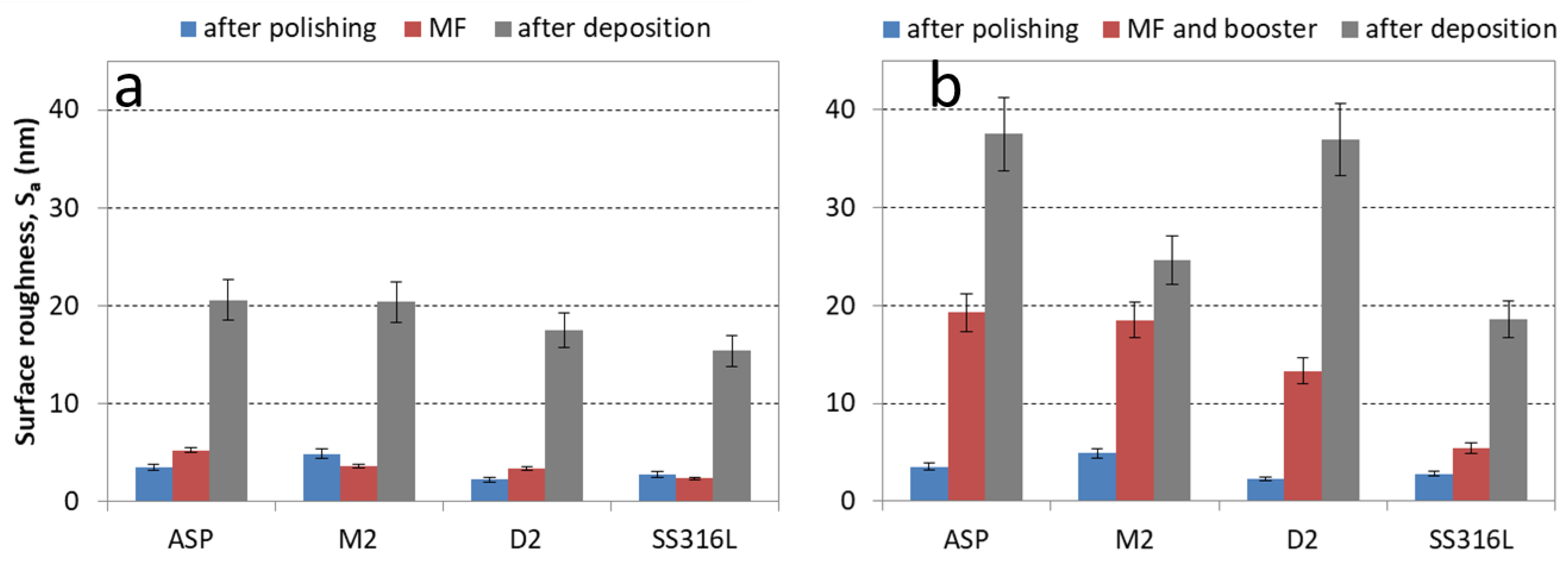
3.2. Interlayer Roughness

Multilayer structures produced by PVD show layer interfaces that are not atomically sharp. Extended boundary regions due to, e.g., interdiffusion or faceting are often visible. The composition, volume and structure of the interlayer regions determine to a large extent the properties and performance of the coating. The coherency of interfaces depends on the crystal structure of materials in contact at the interface. It plays a key role in energy dissipation and stress relaxation. Therefore, the knowledge and control of the quality of interfaces in multilayer structures are important for many applications, especially in optics and microelectronics [24]. For example, interlayer roughness, non-parallel layer interfaces and non-uniformity of the optical constants can significantly affect the optical reflectivity and transmittance of a multilayer coating [25].
In this study, the interlayer roughness was measured on cross-sectional TEM (Figure 2 and Figure 4), STEM (Figure 3) and SEM images (Figure 5) of the NL-TiAlN/CrN coating. Such images provide a more detailed insight into the microstructure and evolution of the interlayer roughness from the substrate–coating boundary to the top surface. Figure 5 shows a cross-sectional scanning electron micrograph of the multilayer obtained with a backscattered electron (BSE) detector. The contrast between the CrN and TiAlN layers is evident because CrN produces more back-scattered electrons, and it is therefore brighter. The thickness of the CrN and TiAlN layers is about 51 nm and 62 nm, respectively. The curvature in the CrN/TiAlN nanolayers reflects the growth front of the coating. The interlayer roughness, which is rather smooth near the substrate, gradually increases up to the coating surface. Cumulative accumulation of the interlayer roughness takes place with the increasing number of bi-layers. It increases more after the deposition of each TiAlN layer, while the upper CrN layer slightly smooths it. This phenomenon can be explained by the crystallographic features of the individual layer material. Namely, the crystal grains of the TiAlN layer are coarser in comparison with the CrN ones (see inset in Figure 5). The TiAlN grains occasionally grow out of the TiAlN layer and continue in the CrN layer (Figure 4). The formation of TiAlN grains larger than the average layer thickness increases the interlayer roughness.
Only a few studies concerning the interlayer roughness in the nanolayer hard coatings can be found in the literature. Recently, Beltrami et al. studied the development of interlayer roughness in nanolayer coatings composed of alternated stoichiometric CrN and understochiometric WN layers [26]. The thickness of individual layers was between 10 nm and 100 nm. All coatings were nanocrystalline with grain sizes in the order of 7 to 20 nm with a face-centered cubic (fcc) crystal structure. They found that the surface roughness of nanolayer coatings is lower in comparison to monolayer CrN coatings of comparable total thickness. The difference is enhanced by reducing the thickness of individual constituent layers, i.e., with a larger number of individual layers. They analyzed the relative contribution of CrN and WN layers to the overall roughness from the SEM image of FIB cross-sections, and they found that the interlayer roughness builds up with the deposition of each additional layer. They also observed that WN layers increase the overall roughness, while CrN layers slightly smoothed the surface. According to their explanation, the alternated deposition of two different material blocks the growth process of crystal grains, resulting in a finer grain size. Therefore, the volume fraction of the amorphous phase at the layer interfaces increases. The presence of the amorphous phase at the interface constrains the growth of crystal grains. Consequently, asperities due to misoriented grains are effectively reduced. Despite the same crystal structure, coherent growth was probably impossible due to a too-large mismatch between the CrN and WN lattices. Their findings generally agree with ours, only the increase in the interlayer roughness with increasing coating thickness is less pronounced than in our case. We explain the difference by the fact that the lattice mismatch in the case of the CrN/WN nanolayer coating is greater than in the case of the NL-TiAlN/CrN coating. Coherent growth within the columnar grain is therefore disabled, and their size is consequently smaller.
Zimmer and Kaufuss showed that, in some cases, the surface of CrN/TiN multilayer coatings prepared by the cathodic arc deposition technique can be smoothed [27]. The individual layer thickness in their nanolayer structure was between 5 and 10 nm. In monolayer CrN or TiN coatings, the size of nodular defects increases with the coating thickness. However, if two different materials are deposited successively, an interface is defined, and a new crystalline structure can start to grow. The precondition is that the new material cannot grow in the same structure or orientation as the droplets, or other types of seed particles incorporated into the coating, during the deposition process. Under such conditions, the nodular defects formed at the site of seed particles are “buried” during further deposition, and after a few layers, a smoothing effect is visible. They also found that the next step to improve the homogeneity of the film structure is a reduction in the individual layer thickness. They explained this phenomenon by the growth of very small crystal grains with random orientations. This was confirmed by X-ray measurements. Namely, they found that in the X-ray spectrum of the CrN/TiN multilayer coating, the intensities of diffraction peaks were strongly reduced in comparison with CrN and TiN monolayers. We did not observe this phenomenon in the case of sputter-deposited NL-TiAlN/CrN coating. The reason could be that the conditions for coherent growth in the NL-TiAlN/CrN coating at the layer interface are more favorable due to a better matching of the lattice parameters than in the case of the CrN/TiN multilayer.

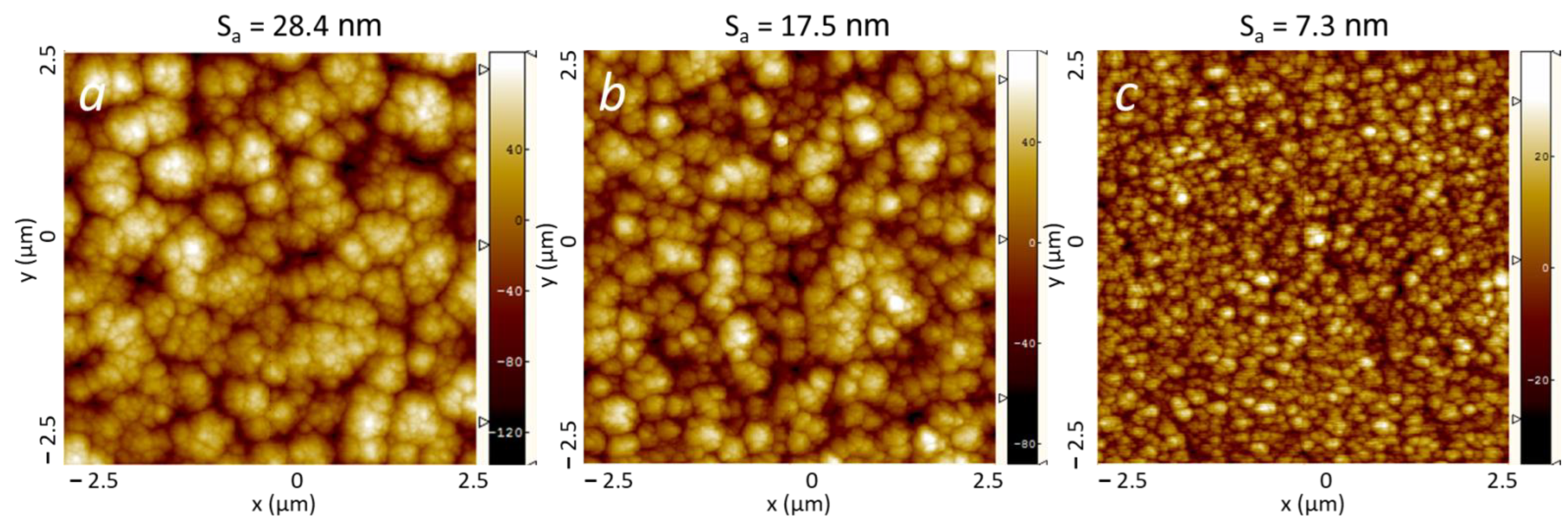
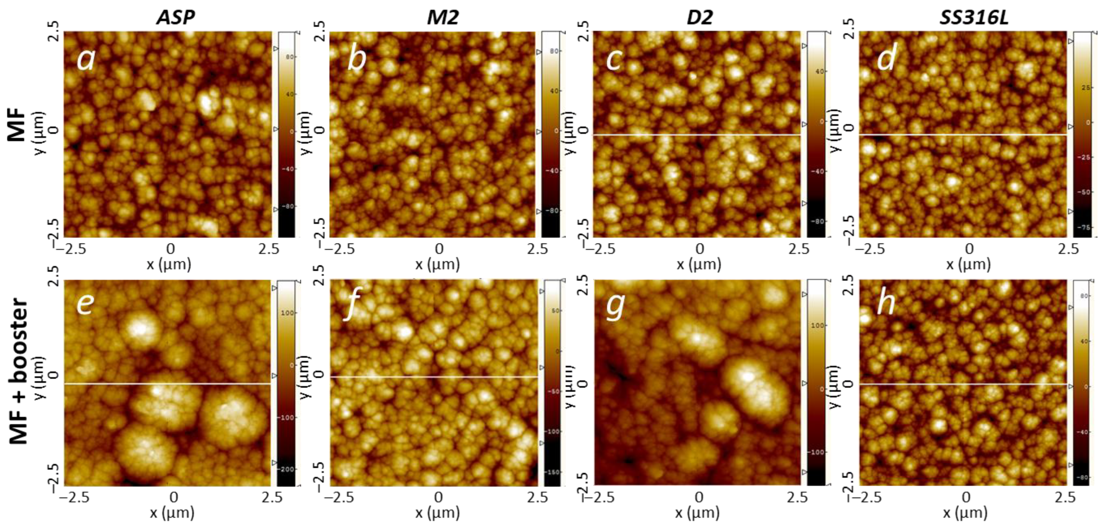
3.3. Surface Topography

Different analytical techniques can be used to characterize the surface morphology of the NL-TiAlN/CrN coating at the micrometer, submicrometer and atomic scale. For example, a 3D image of the coating surface over a large scan area (from a several hundred micrometers square to a several millimeters square) with all the micrometer-sized details can be obtained using a stylus profilometer (Figure 6a). Scanning electron microscopy can be used to look at individual features on the coating surface (Figure 6b), while at the nano level, the surface topography can be evaluated by atomic force microscopy (Figure 6c). In an AFM image, we can resolve the nano-scale sub-cells on the top of every column, which can be further investigated in detail using TEM [9]. The topographical features of the coating surface seen in an AFM image are related to the growth mode.
Figure 7 shows the SEM images of the same surface area of the steel substrates ASP30, M2, D2 and SS316L after polishing, MF and booster ion etching and deposition of the NL-TiAlN/CrN hard coating. All carbide and non-metallic inclusions on the polished surface of all four bare substrates were identified by EDX analysis. By comparing SEM images of the same surface of the substrate, we followed the topographical changes at the sites of these inclusions.
During polishing, the removal rate of harder inclusions (e.g., carbides or oxides) is lower than the matrix; however, it is higher if inclusions are softer than the matrix (e.g., sulfides) [7,8]. Therefore, shallow protrusions and craters are formed at these sites. A similar effect arises during ion etching. In this case, the sputtering yield determines the etching rate of various types of inclusions and the matrix. After polishing and ion etching, the geometrical extension from the matrix level (typically up to a few hundred nanometers either in a positive or a negative direction) at the site of inclusions depends on the net removal rate [7,8]. The height of protrusions and depth of craters are much larger if a more intensive booster etching is used. If the net removal rate is higher than that of the matrix, the inclusion appears like a shallow crater, and after coating deposition, pinholes form at these sites. If it is lower than that of the matrix, the inclusion appears like a shallow protrusion, where a nodular defect forms after deposition. It is also possible that the net removal rates of the selected inclusion and matrix are similar. In this case, no geometric effect can be expected.
During the deposition process, all topographical irregularities on the substrate surface formed during polishing and ion etching are transferred onto the coating surface and are often magnified due to the geometrical shadowing effect. However, after the deposition of the coating, its surface roughness increases significantly due to the formation of growth defects. At a high magnification of the area between growth defects and inclusions (see insets in Figure 7), we did not notice any significant difference in the surface topography of coatings deposited on the four different types of substrates (ASP, M2, D2 and SS316L). Columns with dome-shaped tops of comparable size can be observed, regardless of the type of the substrate. This is probably because the roughness of the matrix of all four types of substrates after ion etching is comparable, while the intensity of ion bombardment during the deposition process is identical. However, the surface topography of the NL-TiAlN/CrN coating is considerably different for samples prepared by different rotation modes (Figure 8). The topography of the coating surface prepared by different rotation modes reflects their microstructural differences, as described in Section 3.1.
Figure 9a shows the AFM surface roughness measured on the substrate after polishing, MF ion etching and deposition. Figure 9b shows similar measurements where MF and booster etching technique were applied. The roughness measurements were performed on an area of 20 µm × 20 µm where no growth defects were present. We can see that after MF ion etching, the roughness increases only a little. However, it increases significantly after the deposition of the coating. On samples etched by the MF and booster technique, the roughness increases significantly after both ion etching and deposition.
We also checked whether different etching methods affect the surface topography in the coating area without growth defects. For this test, one set of the substrates was cleaned in a separate batch using standard mid-frequency (MF) ion etching, while another set of substrates was cleaned by the more intensive booster etching. After that, both sets of substrates were loaded again in the deposition system where they were once more cleaned by MF ion etching for 10 min to remove any possible impurities that formed during the previous analysis. This was followed by the deposition of the NL-TiAlN/CrN coating. Figure 10 shows the AFM images of the surface topography of the coatings deposited on four different substrate materials, which were previously cleaned by two different ion etching procedures. No significant difference in surface topography can be observed. The larger clusters in Figure 10e,g have grown on the sites of carbide inclusions in the ASP and D2 substrates.

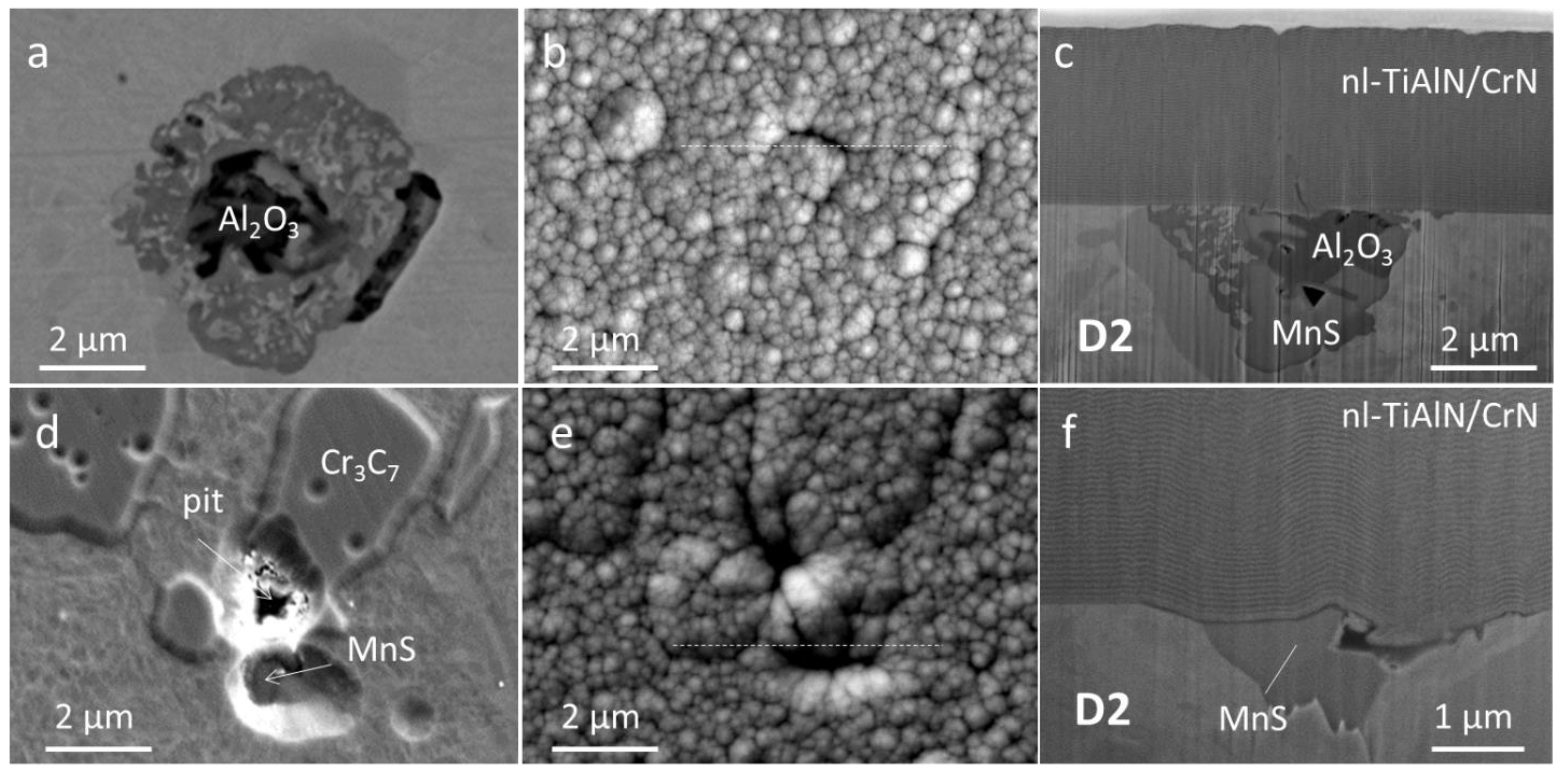
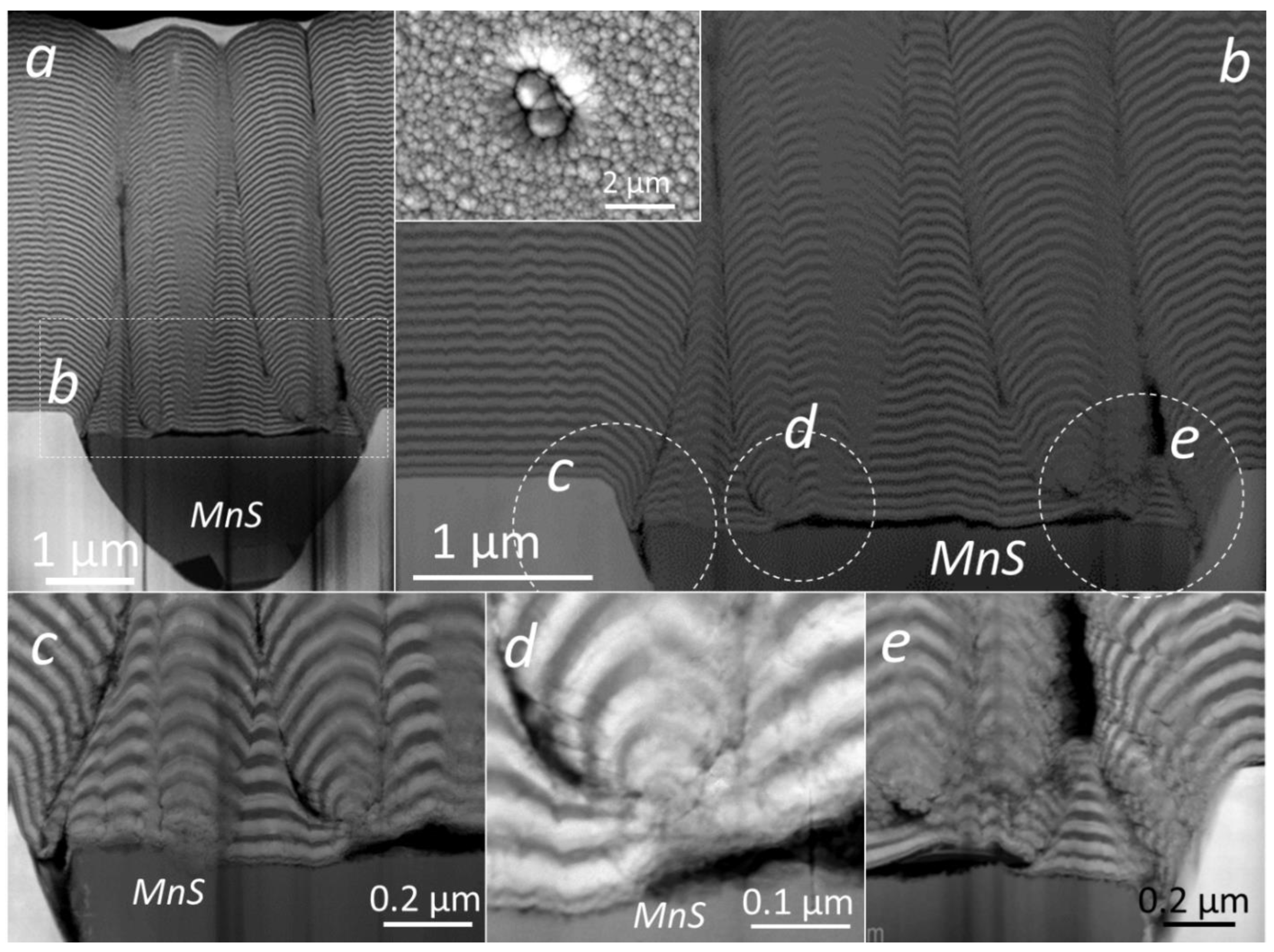
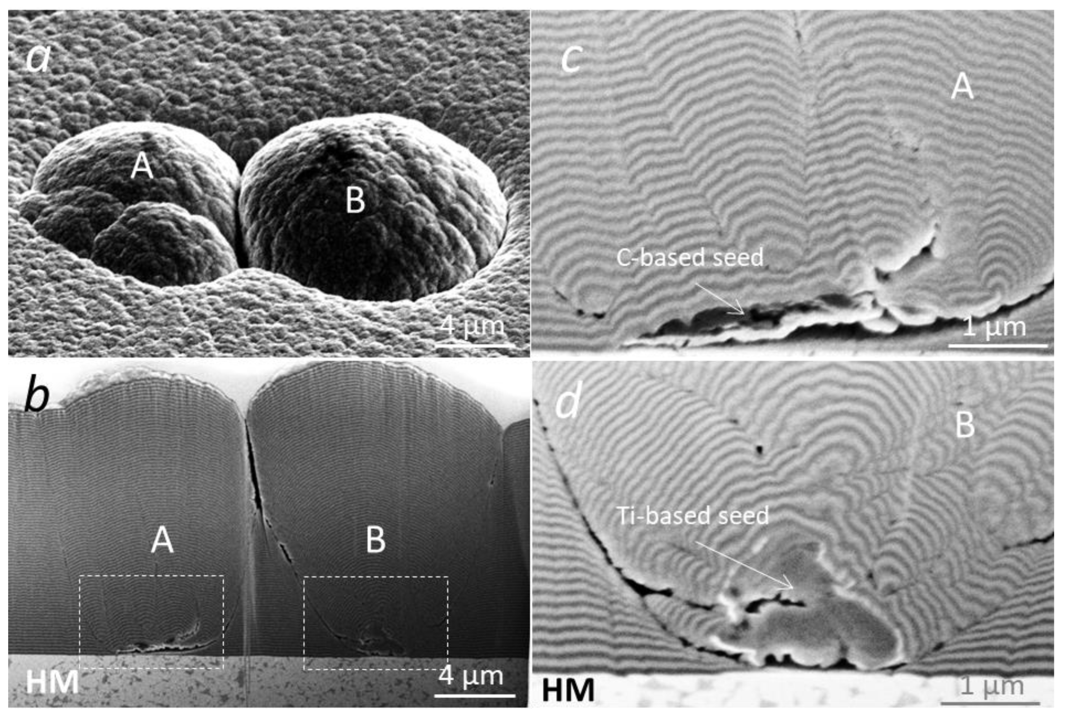
3.4. Formation of Growth Defects

The largest increase in coating surface roughness is caused by growth defects formed on different substrate surface irregularities. One origin of irregularities is a result of substrate pretreatment (grinding, polishing and ion etching). As was explained in the previous section, topographical irregularities in the inhomogeneous substrate material, such as tool steel, are formed at the sites of inclusions (e.g., carbide and non-metallic inclusions, see Figure 7). While the carbides are an essential component of tool steels, the non-metallic inclusions are undesired products formed during the steel production. All steels contain non-metallic inclusions to some extent, as they precipitate during the cooling and solidification of the steel [28]. They can vary widely in size, shape and composition. The typical dimensions of inclusions are in the range of 0.1–100 μm. Non-metallic inclusions that form separate phases are the chemical compounds of metals (e.g., iron, manganese, aluminum, silicon and calcium) with oxygen, sulfur, carbon, hydrogen or nitrogen. The majority of the inclusions in steels are oxides and sulfides [7]. The type of non-metallic inclusions depends on the steel grade, steel-making process, secondary metallurgy treatments and casting of steel. Though the concentration of non-metallic inclusions is low (less than 0.01%), they have a significant effect on steel properties. Namely, a high density of coarse inclusions can cause the formation of cracks and, thus, initiates fracture and decreases the toughness of steels [29]. Surface defects caused by them deteriorate mechanical properties such as corrosion resistance, deformability, brittle fracture and fatigue strength. They also affect the weldability, polishability and machinability of the steel.
In principle, the coating surface is a conformal replication of the substrate surface. Therefore, all protrusions and cavities formed during substrate pretreatment are transferred to the coating surface (Figure 7, Figure 11 and Figure 12). Even if the inclusions have a similar net removal rate as the matrix, they can affect the growth of the coating because they are chemically and structurally different from the matrix.
The largest nodular defects formed on foreign particles and droplets, which arrived on the substrate surface before or during the coating growth. Due to the geometrical shadowing effect, characteristic of the PVD deposition processes, the initial small seed particle is growing during the deposition of the coating (Figure 13 and Figure 14). While a smaller portion of defects formed on seed particles embedded on the layer during the deposition process (Figure 14), a larger portion of defects formed on seed particles that were on the surface of the substrate, even before the start of the deposition (Figure 13). This is evident from a low-angle cross-section of the NL-TiAlN/CrN coating, prepared by the ball cratering technique, where the layer contours reveal the positions of defects (Figure 15). In our recently published paper, we showed that the distribution of nodular defects on the ground section of the NL-TiAlN/CrN coating is uniform, which means that most nodular defects started to grow at the substrate–coating interface [30]. The complex shapes of contours in the SEM image of the nodular defects’ ground section reveal their internal structure (Figure 15e–g), which results from the growth of nodular defects on seeds with irregular geometry. Namely, the contours of individual layers in the multilayer coating follow the shape of the seed. The nodular defects are composed of several columns that start to grow on different parts of the seed particle independently of each other (Figure 13c,d).

4. Conclusions

The goal of this study was to better understand the growth and morphology of the NL-TiAlN/CrN coating sputter deposited on four different types of steels and cemented carbide substrates. We studied the microstructure, surface topography, layer periodicity, interlayer roughness and formation of growth defects at the sites of non-metallic inclusions and foreign seeds. Furthermore, these properties were analyzed with dependence on the substrate rotation mode, the type of the substrate material and method of ion etching. The results of our investigation can be summarized as follows:
  • The microstructure, topography and periodicity of the NL-TiAlN/CrN hard coating strongly depend on the rotation mode. The coatings prepared by one-fold rotation have a periodic structure and a pronounced columnar microstructure that extends from the substrate to the coating surface. On the other hand, coatings prepared by three-fold rotation have an aperiodic, less columnar (with much smaller average column diameters) and a fine-grained microstructure.
  • A coherent growth of TiAlN and CrN layers inside the columnar grains was observed.
  • The conformity and uniformity of multilayer coating were analyzed from SEM images of the FIB cross-sections. The curvature of individual layers in the multilayer coating reflects the growth front of the coating. Although the initial roughness at the interface between the first layer and the substrate was rather small, it accumulated during deposition and gradually increased towards the top of the coating.
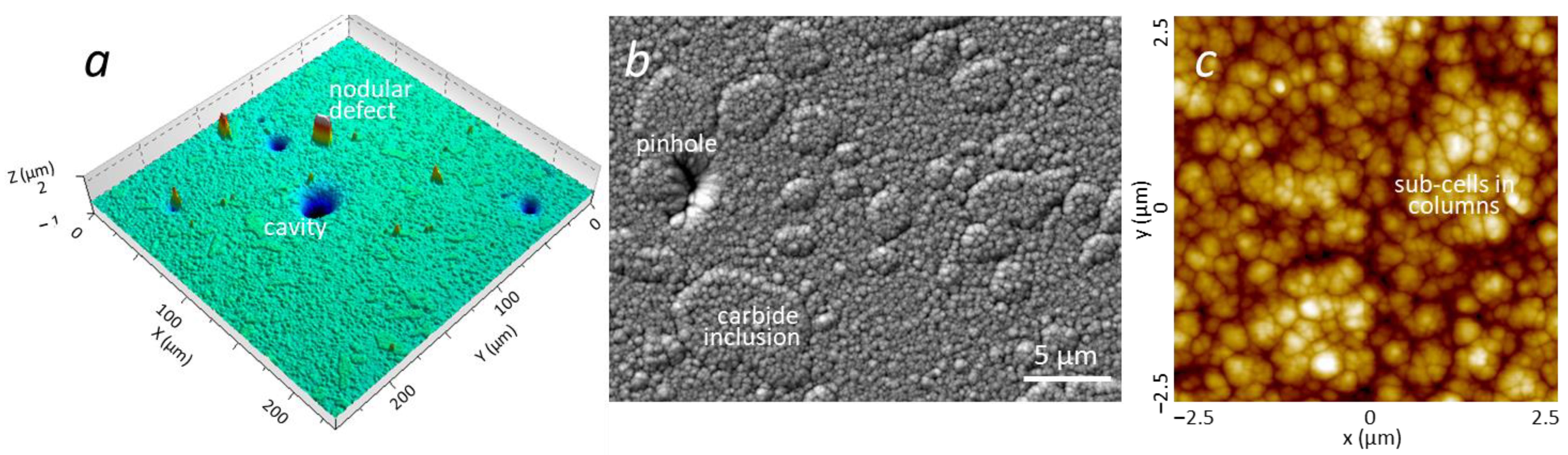
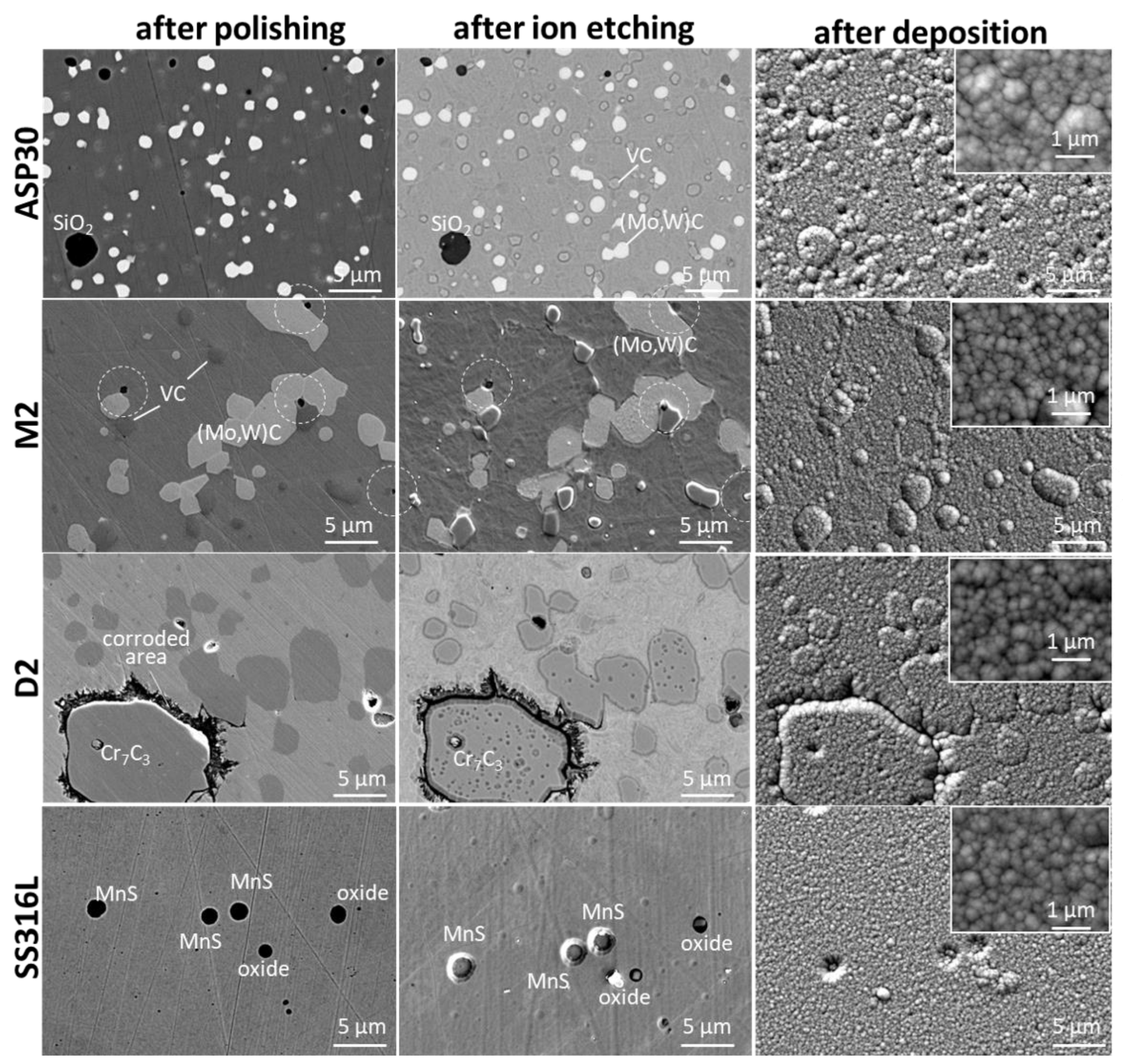
  • Shallow craters or protrusions formed at the sites of non-metallic inclusions in the steel substrates, depending on whether the net removal rate after polishing and ion etching was higher or lower compared to the matrix. Even if the net removal rate of both materials is similar, the non-metallic inclusions can affect the growth of the coating, as they are chemically and structurally different from the matrix. The influence of non-metallic inclusions on the microstructure and topography of the layer is also not negligible because they can cause a local loss of adhesion, pitting corrosion and other destructive effects.
  • The largest increase in the coating roughness is due to the presence of nodular defects formed on seed particles that arrive on the substrate surface during its pretreatment or deposition. We showed that the majority of nodular defects start to grow at the substrate-coating interface, i.e., on particles that arrive on the substrate before the start of the deposition. We also demonstrated that the contours of the individual layers in the multilayered coating reveal the internal structure of the nodular defect. The irregular shapes of layer contours are the result of the complex geometry of the seed particles and the geometrical shadowing effect during the deposition.

Author Contributions

Design of experiments, 3D profilometry, interpretation of experimental results, manuscript writing and project administration, P.P.; design of experiment, preparation of specimen for TEM characterization, SEM analysis and manuscript review, P.G.; SEM and FIB analysis and manuscript review, T.B. and F.Z.; AFM, SEM and FIB analysis and manuscript review, A.D.; preparation of specimen for TEM characterization, manuscript review and project administration, M.P.; STEM investigations and data analysis, M.A.; manuscript review, M.Č. All authors have read and agreed to the published version of the manuscript.

Funding

This work was supported by the Slovenian Research Agency (program P2-0082, project J2-2509). We also acknowledge funding from the European Regional Development Funds (CENN Nanocenter, OP13.1.1.2.02.006) and the European Union Seventh Framework Programme under Grant Agreement 312483-ESTEEM2 (Integrated Infrastructure Initiative-I3).

Institutional Review Board Statement

Not applicable.

Informed Consent Statement

Not applicable.

Data Availability Statement

Not applicable.

Acknowledgments

The authors would also like to thank Martina Dienstleder (Graz Centre for Electron Microscopy, Graz, Austria) for the preparation of specimens for STEM analysis using the focused ion beam (FIB) workstation and Jožko Fišer (Jožef Stefan Institute, Ljubljana, Slovenia) for technical assistance.

Conflicts of Interest

The authors declare no conflict of interest.

References

  1. Harlin, P.; Carlsson, P.; Bexell, U.; Olsson, M. Influence of surface roughness of PVD coatings on tribological performance in sliding contacts. Surf. Coat. Technol. 2006, 201, 4253–4259. [Google Scholar] [CrossRef]
  2. Olofsson, J.; Gerth, J.; Nyberg, H.; Wiklund, U.; Jacobson, S. On the Influence from Micro Topography of PVD Coatings on Friction Behaviour, Material Transfer and Tribofilm Formation. Wear 2011, 271, 2046–2057. [Google Scholar] [CrossRef]
  3. Saketi, S.; Östby, J.; Olsson, M. Influence of tool surface topography on the material transfer tendency and tool wear in the turning of 316L stainless s steel. Wear 2016, 368–369, 239–252. [Google Scholar] [CrossRef]
  4. Panjan, P.; Drnovšek, A.; Kovač, J. Tribological Aspects Related to the Morphology of PVD Hard Coatings. Surf. Coat. Technol. 2018, 343, 138–147. [Google Scholar] [CrossRef]
  5. Luo, Q. Origin of Friction in Running-in Sliding Wear of Nitride Coatings. Tribo. Lett. 2010, 37, 529–539. [Google Scholar] [CrossRef]
  6. Panjan, P.; Drnovšek, A.; Terek, P.; Miletić, A.; Čekada, M.; Panjan, M. Comparative Study of Tribological Behavior of TiN Hard Coatings Deposited by Various PVD Deposition Techniques. Coatings 2022, 12, 294. [Google Scholar] [CrossRef]
  7. Panjan, P.; Drnovšek, A.; Gselman, P.; Čekada, M.; Panjan, M. Review of Growth Defects in Thin Films Prepared by PVD Techniques. Coatings 2020, 10, 447. [Google Scholar] [CrossRef]
  8. Panjan, P.; Drnovšek, A.; Mahne, N.; Čekada, M.; Panjan, M. Surface Topography of PVD Hard Coatings. Coatings 2021, 11, 1387. [Google Scholar] [CrossRef]
  9. Panjan, P.; Drnovšek, A.; Dražić, G. Influence of Growth Defects on the Oxidation Resistance of Sputter-Deposited TiAlN Hard Coatings. Coatings 2021, 11, 123. [Google Scholar] [CrossRef]
  10. Nordin, M.; Ericson, F. Growth characteristics of multilayered physical vapour deposited TiN/TaNx on high speed steel substrates. Thin Solid Film. 2001, 385, 174–181. [Google Scholar] [CrossRef]
  11. Xu, Y.X.; Chen, L.; Fei, P.; Chang, K.K.; Yong, D. Effect of the modulation ratio on the interface structure of TiAlN/TiN and TiAlN/ZrN multilayers: First-principles and experimental investigations. Acta Mater. 2017, 130, 281–288. [Google Scholar] [CrossRef]
  12. Panjan, M.; Šturm, S.; Panjan, P.; Čekada, M. TEM investigation of TiAlN/CrN multilayer coatings prepared by magnetron sputtering. Surf. Coat. Technol. 2007, 202, 815. [Google Scholar] [CrossRef]
  13. Xu, Y.X.; Chen, L.; Pei, F.; Du, Y. Structure and thermal properties of TiAlN/CrN multilayered coatings with various modulation ratio. Surf. Coat. Technol. 2016, 304, 512–518. [Google Scholar] [CrossRef]
  14. Helmersson, U.; Todorova, S.; Barnett, S.A.; Sundgren, J.-E.; Markert, L.C.; Greene, J.E. Growth of single-crystal TiN/VN strained-layer superlattices with extremely high mechanical hardness. J. Appl. Phys. 1987, 62, 481. [Google Scholar] [CrossRef]
  15. Barshilia, H.C.; Prakash, M.S.; Jain, A.; Rajam, K.S. Structure, hardness and thermal stability of TiAlN and nanolayered TiAlN/CrN multilayer films. Vacuum 2005, 77, 169–179. [Google Scholar] [CrossRef]
  16. Park, J.K.; Park, H.J.; Ahn, J.H.; Baik, Y.J. Effect of Ti to Al ratio on the crystalline structure and hardening of a Ti1−xAlxN/CrN nanoscale multilayered coating. Surf. Coat. Technol. 2009, 203, 3099–3103. [Google Scholar] [CrossRef]
  17. Waddsworth, I.; Smith, I.J.; Donohue, L.A.; Munz, W.D. Thermal stability and oxidation resistance of TiAlN/CrN multilayer coatings. Surf. Coat. Technol. 1997, 94–95, 315–321. [Google Scholar] [CrossRef]
  18. Povstugar, I.; Pyuck-Pa, C.; Darius, T.; Jae-Pyeong, A.; Dierk, R. Interface-directed spinodal decomposition in TiAlN/CrN multilayer hard coatings studied by atom probe tomography. Acta Mater. 2013, 61, 7534–7542. [Google Scholar] [CrossRef]
  19. Wei, Y.; Zong, X.; Jiang, Z.; Tian, X. Characterization and mechanical properties of TiN/TiAlN multilayer coatings with different modulation periods. Int. J. Adv. Manuf. Technol. 2018, 96, 1677–1683. [Google Scholar] [CrossRef]
  20. Panjan, M.; Peterman, T.; Čekada, M.; Panjan, P. Simulation of a multilayer structure in coatings prepared by magnetron sputtering. Surf. Coat. Technol. 2009, 204, 850–853. [Google Scholar] [CrossRef]
  21. Panjan, M. Influence of substrate rotation and target arrangement on the periodicity and uniformity of layered coatings. Surf. Coat. Technol. 2013, 235, 32–44. [Google Scholar] [CrossRef]
  22. Pennycook, S.J.; Jesson, D.E. High-resolution Z-contrast imaging of crystals. Ultramicroscopy 1991, 37, 14–38. [Google Scholar] [CrossRef] [Green Version]
  23. Rother, B.; Jehn, H.A.; Gabriel, H.M. Multilayer hard coatings by coordinated substrate rotation modes in industrial PVD deposition systems. Surf. Coat. Technol. 1996, 86–87, 207–211. [Google Scholar] [CrossRef]
  24. Esashi, Y.; Tanksalvala, M.; Zhang, Z.; Jenkins, N.W.; Kapteyn, H.C.; Murnane, M.M. Influence of surface and interface roughness on X-ray and extreme ultraviolet reflectance: A comparative numerical study. OSA Contin. 2021, 4, 1497–1518. [Google Scholar] [CrossRef]
  25. Kaiser, N. Review of the Fundamentals of Thin-Film Growth. Appl. Opt. 2002, 41, 3053–3060. [Google Scholar] [CrossRef]
  26. Beltrami, M.; Zilio, S.D.; Kapun, G.; Ciubotaru, C.D.; Rigoni, F.; Lazzarino, M.; Sbaizero, O. Surface roughness control in nanolaminate coatings of chromium and tungsten nitrides. Micro Nano Eng. 2022, 14, 100107. [Google Scholar] [CrossRef]
  27. Zimmer, O.; Kaulfuß, F. Hard Coatings with High Film Thickness Prepared by PVD. Plasma Process. Polym. 2009, 6, S152–S156. [Google Scholar] [CrossRef]
  28. da Costa e Silva, A.L.V. Non-metallic inclusions in steels—Origin and control. J. Mater. Res. Technol. 2018, 7, 283–299. [Google Scholar] [CrossRef]
  29. Murakami, Y. Metal Fatigue: Effects of Small Defects and Nonmetallic Inclusions; Elsevier Science Ltd.: Oxford, UK, 2002; pp. 75–122. [Google Scholar]
  30. Panjan, P.; Drnovšek, A.; Čekada, M.; Panjan, M. Contamination of Substrate Coating Interface Caused by Ion Etching. Coatings 2022, 12, 846. [Google Scholar] [CrossRef]
Figure 1. Fracture cross-sectional SEM images of NL-TiAlN/CrN hard coating sputter deposited on cemented carbide substrates. The samples were prepared in the same batch but rotated around a different number of axes: (a) one-fold, (b) two-fold and (c) three-fold rotation. The magnification scales are identical.
Coatings 12 01725 g001
Figure 2. Cross-sectional TEM images of NL-TiAlN/CrN hard coating with a typical columnar grain growth and sputter deposited on cemented carbide substrates. The samples were prepared in the same batch but rotated around a different number of axes: (a) one-fold, (b) two-fold and (c) three-fold rotation. The magnification scales are identical.
Coatings 12 01725 g002
Figure 3. High-angle annular dark-field (HAADF) STEM image (Z-contrast image) of the NL-TiAlN/CrN hard coating sputter deposited on an Al2O3 inclusion in the D2 tool steel substrate using the two-fold rotation (a) and EDS line scan along the dashed red line indicated in the STEM image (b).
Coatings 12 01725 g003
Figure 4. Bright- (a) and dark- (b) field TEM images of the same area of the NL-TiAlN/CrN hard coating deposited on cemented carbide substrate using the three-fold rotation; (c) high resolution TEM image of the area inside of the frame; the lattice fringes clearly show coherency between the layers.
Coatings 12 01725 g004
Figure 5. Bright-field cross-sectional SEM image of the NL-TiAlN/CrN coating deposited on cemented carbide substrate using the two-fold rotation (a). The interlayer roughness gradually increases up to the top of the coating. Crystal grains in both types of layers are clearly visible in the inset TEM image (b). The area marked with the dashed frame is shown at higher magnification in bright-field cross-sectional STEM image (c). The first increase in interlayer roughness occurs in the TiAlN layer (see sites marked with arrows).
Coatings 12 01725 g005
Figure 6. Surface topography appearance of the NL-TiAlN/CrN hard coating sputter deposited on the D2 tool steel substrate using three different surface analytical techniques: (a) 3D profile image of a scanning area of 250 µm × 250 µm, (b) plain-view SEM image of an area ten times smaller and (c) AFM image at a scanning area of 5 µm × 5 µm.
Coatings 12 01725 g006
Figure 7. Top-view SEM images of the same surface area of ASP30, M2, D2 and SS316L steel substrates after polishing, ion etching (MF and booster) and deposition of the NL-TiAlN/CrN hard coatings. SEM images of the coating morphology at high magnification are shown in the insets.
Coatings 12 01725 g007
Figure 8. AFM images (scan area 5 µm × 5 µm) show the surface morphology of the NL-TiAlN/CrN hard coating sputter deposited on D2 tool steel substrates. The samples were prepared in the same batch but rotated around a different number of axes: (a) one-fold, (b) two-fold and (c) three-fold rotation.
Coatings 12 01725 g008
Figure 9. AFM surface roughness of four different steel substrates (ASP, M2, D2, SS 316L) after polishing, ion etching and deposition. One set of substrates was ion etched by the MF technique (a) while the other one by MF and booster (b). The scan area was 20 µm × 20 µm.
Coatings 12 01725 g009
Figure 10. AFM images of surface morphology of the NL-TiAlN/CrN coating deposited in the same batch on four different steel substrates (ASP30, M2, D2 and SS316L) ion etched by MF (top row) and MF and booster techniques (bottom row).
Coatings 12 01725 g010
Figure 11. Plain-view SEM images of the same surface area at the site of a complex multicomponent non-metallic inclusion in a D2 tool steel substrate after MF ion etching (a), deposition of the NL-TiAlN/CrN coating (b) and FIB cross-sections of the coating (c). Similar SEM images were taken at the site of a MnS inclusion in the D2 tool steel substrate after MF and booster ion etching (d), deposition of the NL-TiAlN/CrN coating (e) and FIB cross-sections of the coating (f).
Coatings 12 01725 g011
Figure 12. STEM images of the FIB cross-section of the NL-TiAlN/CrN hard coating at the site of a MnS inclusion in the stainless steel SS316L substrate (ae). A shallow crater (a), which is formed at this site after booster ion etching, is the starting point for a pinhole formation at the boundary between the inclusion and the matrix. An additional effect is poor contact of the coating to the inclusion surface. We can also see nodular defects that have formed on smaller seed particles located at the bottom of the crater (ce).
Coatings 12 01725 g012
Figure 13. Top view SEM image (a) and SEM images of FIB cross-sections (b) of the nodular defects in the NL-TiAlN/CrN coating. The left nodular defect formed at the site of a carbon-based particle (c), while the right one was at a titanium-based particle (d). A small step on the substrate surface beneath the titanium-based particle proves that it arrived on the substrate surface during the ion etching process.
Coatings 12 01725 g013
Figure 14. Top-view SEM images (a,b) and SEM images of the FIB cross-sections (cf) of three nodular defects (A–C) in the NL-TiAlN/CrN coating. All three defects formed at the site of Cr-based flakes, which were incorporated in the coating at the same depth. All three flakes probably came from the same source. We believe that they originate from arcs occurring at the perimeter of the chromium target.
Coatings 12 01725 g014
Figure 15. Optical microscopy images at lower (a) and higher (bd) magnifications of a low-angle cross-section of the NL-TiAlN/CrN coating, prepared by the ball cratering technique. SEM images of the ground section of selected nodular defects (eg) reveal their internal structure due to the complex geometry of seed particles.
Coatings 12 01725 g015
Publisher’s Note: MDPI stays neutral with regard to jurisdictional claims in published maps and institutional affiliations.

