
Dielectric and Antiferroelectric Properties of AgNbO3 Films Deposited on Different Electrodes


1
Key Laboratory of High-Precision Computation and Application of Quantum Field Theory of Hebei Province, College Physics Science & Technology, Hebei University, Baoding 071002, China
2
State Key Laboratory of New Ceramics and Fine Processing, School of Materials Science and Engineering, Tsinghua University, Beijing 100084, China
3
Foshan (Southern China) Institute for New Materials, Foshan 528247, China
*
Authors to whom correspondence should be addressed.
Coatings 2022, 12(12), 1826; https://doi.org/10.3390/coatings12121826
Submission received: 6 October 2022
/
Revised: 21 November 2022
/
Accepted: 23 November 2022
/
Published: 25 November 2022
(This article belongs to the Special Issue High-Performance Dielectric Ceramic for Energy Storage Capacitors)
Abstract
:AgNbO3 antiferroelectric materials have become a hot topic due to their typical double polarization–electric field loops. AgNbO3 films usually exhibit superior properties to bulks. In this work, AgNbO3 films were fabricated via the pulsed laser deposition on (001) SrTiO3 substrate with (La0.5Sr0.5)CoO3, LaNiO3 and SrRuO3 bottom electrodes, in which the (La0.5Sr0.5)CoO3, LaNiO3 and SrRuO3 bottom electrodes were used to regulate the in-plane compressive stress of AgNbO3 films. It is found that AgNbO3 films deposited on (La0.5Sr0.5)CoO3, LaNiO3 and SrRuO3 bottom electrodes are epitaxial with dense microstructure. In changing the bottom electrodes from (La0.5Sr0.5)CoO3, LaNiO3 to SrRuO3, the in-plane compressive stress of AgNbO3 thin films becomes weaker, which leads to increased relative dielectric permittivity and reduced antiferroelectric–ferroelectric phase transition electric field EF from 272 kV/cm to 190 kV/cm. The reduced EF implies weakened antiferroelectric stability in AgNbO3 films. It can be seen that the antiferroelectric stability of AgNbO3 films could be regulated by changing the bottom electrodes.
1. Introduction
AgNbO3-based ceramics, as lead-free antiferroelectric (AFE) materials, have aroused enormous interest in dielectric energy storage [1,2,3,4,5,6]. Besides its multifunctionality, AgNbO3 is an intriguing system due to its rich phase structures in sequence of:
where, the cubic C phase, tetragonal T phase and orthorhombic O phase are high-temperature paraelectric (PE) phases, both M2 and M3 phases are AFE, while M1 phase is ferrielectric (FIE) phase dominated by the AFE phase caused by the non-centrosymmetric structure of Pmc21 space group [7]. Since the M1-M2 phase transition temperature is normally above room temperature, AgNbO3 ceramics usually show FIE M1 phase at room temperature, which leads to a non-zero remnant polarization Pr and hysteresis in polarization–electric field (P-E) loops. The AFE stability of AgNbO3-based ceramics can be enhanced by stabilizing M2 or M3 phase at room temperature via ions doping [8,9,10]. For example, Sm-doping or La-doping can lead to M1-M2 phase transition at room temperature and thus enhance the AFE stability in AgNbO3-based ceramics [8,9]. Higher AFE stability can be realized in Ta-doped AgNbO3 ceramics due to the reduced polarizability of B-site cation and stabilized M2 phase at room temperature [10]. While in contrast, Li-doping or K-doping can enhance the ferroelectric (FE) property in AgNbO3 ceramics owing to the AFE-FE phase transition [11,12]. For example, a strong local polarization can be effectively induced by Li-substitution in AgNbO3 ceramics, which favor a rhombohedral distortion [11]. A strong FE state is realized in K-doped AgNbO3 ceramics [12]. Beside ions doping, the AFE/FE property of the AgNbO3-based ceramics can be affected by pressure. AgNbO3 ceramic shows enhanced AFE property as under an applied hydrostatic pressure, which is confirmed by the increased AFE-FE phase transition electric field EF and FE-AFE phase transition electric field EA [13]. (Ag0.935K0.065)NbO3 ceramics are FE state when the applied hydrostatic pressure is 0 MPa and AFE state when the applied hydrostatic pressure is 300 MPa, indicating a pressure-driven FE-AFE phase transition [14]. In addition, the AFE/FE property strongly depends on the orientation in AgNbO3 films [15]. In 2010, Sakurai et al. prepared AgNbO3 films on (001), (110) and (111) SrTiO3 substrates with SrRuO3 bottom electrodes, but their P-E loops are not symmetrical. It is found that the P-E hysteresis behaviors of the AgNbO3 films depend on the orientation directions. All AgNbO3 films show a weak FE property under a very small applied electric field. AgNbO3 film deposited on (001) SrTiO3 shows AFE property at 100–350 kV/cm. AgNbO3 film deposited on (110) SrTiO3 shows AFE property at 150 kV/cm and FE property at above 200 kV/cm. AgNbO3 film deposited on (111) SrTiO3 shows FE property at 100–350 kV/cm [15]. In 2021, Zhang et al. prepared AgNbO3 films on (La0.5Sr0.5)CoO3/SrTiO3 substrates [5], in which obvious double P-E loops were observed when the applied electric field is higher than 300 kV/cm, indicating AFE property. In 2022, Shu et al. prepared AgNbO3 films on Pt/Ti/SiO2/Si substrates via the chemical solution deposition, which revealed AFE M2 phase at room temperature. Unfortunately, no double P-E loops were observed in these AgNbO3 films due to their small breakdown strength Eb of less than 110 kV/cm [16]. Up to now, although AgNbO3 films have been reported in some of the literature, it is still challenging to achieve typical double P-E loops in AgNbO3 films. On the other hand, first-principle calculations proposed that the AFE stability of epitaxial AgNbO3 films can be affected by the in-plane compressive stress, which can be inferred by EA and EF [17]. The in-plane compressive stress comes from the lattice mismatch between the AgNbO3 films and the bottom electrodes or substrates. In other words, the in-plane compressive stress can be regulated by the bottom electrodes or substrates. The enhanced AFE stability is conducive to obtaining the typical double P-E loops and high energy storage performance in AgNbO3 films. Thus, it is necessary to figure out the relationship between the in-plane compressive stress and the AFE stability in AgNbO3 films.
In this work, AgNbO3 films were deposited on (La0.5Sr0.5)CoO3, LaNiO3 and SrRuO3 bottom electrodes to investigate the effect of in-plane compressive stress on the AFE stability. It is found that EF decreased from 272 kV/cm to 190 kV/cm when changing the bottom electrodes from (La0.5Sr0.5)CoO3, LaNiO3 to SrRuO3, indicating weakened AFE stability, which may be caused by the reduced in-plane compressive stress.
2. Experimental Procedure
AgNbO3 (ANO) epitaxial thin films were fabricated via pulsed laser deposition (PLD) on (001) SrTiO3 (STO) substrates. Prior to the fabrication of ANO films, the epitaxial (La0.5Sr0.5)CoO3 (LSCO), LaNiO3 (LNO) and SrRuO3 (SRO) layers, with a thickness of about 40 nm, were deposited on STO substrates by radio frequency magnetron sputtering as bottom electrodes. Firstly, the clean STO substrate was placed in the chamber of the magnetron sputtering instrument, the gas was extracted to 2 × 10⁻⁴ Pa, and then argon and oxygen were filled with a volume ratio of 3:1. The deposition temperature, radio frequency power and total pressure were 700 °C, 50 W and 3 Pa, respectively. The distance between the target and the substrate was kept at 5.4 cm. LSCO, LNO and SRO films with ~40 nm in thickness are deposited on (001) STO substrate, respectively. Then, the LSCO/STO, LNO/STO and SRO/STO substrates were placed into a vacuum chamber; high-purity oxygen was piped into the chamber till 7.6 Pa was achieved. A ~500 nm ANO film was fabricated on the LSCO/STO, LNO/STO and SRO/STO substrates via the PLD with the laser frequency and power of 3 Hz and 0.72 W. The distance between target and substrate target was 4.5 cm; the growth temperature was 550 °C. After deposition, the as-grown film was gradually cooled down to room temperature in 8 × 10⁴ Pa oxygen pressure. The top LSCO, LNO and SRO symmetry electrodes and Pt electrode were prepared through a metal shadow mask with a diameter of 100 mm by radio frequency magnetron sputtering at room temperature. Then, the as-grown films were annealed at 550 °C in high-purity oxygen for 1 h.
The crystallographic structure and orientation of the ANO films were checked by X-ray diffraction (XRD, D8 Advance, Saarbruken, Germany) with Cu Ka radiation (λ = 0.15406 nm). The angle range, rate and step size of the XRD are 20–80°, 1.2°/min and 0.02°. The surface morphology of the ANO films was examined by scanning electron microscopy (SEM, NovaNano SEM450, Hillsborough, OR, USA). The SEM acceleration voltage was 15 kV. The relative dielectric constant and dielectric loss of the ANO films were measured by LCR tester (Radiant Technologies, Albuquerque, NM, USA). The dielectric spectroscopy frequency range is from 103 Hz to 106 Hz, and the oscillation voltage is 1 V. A ferroelectric tester (Precision LC II, Radiant Technologies, Albuquerque, NM, USA) was used to study the AFE properties of the ANO films with a frequency of 104 Hz.
3. Results and Discussion
The crystal structures of ANO films grown on LSCO, LNO and SRO bottom electrodes were measured by XRD, as shown in Figure 1. The ANO films grown on LSCO, LNO and SRO bottom electrodes show (002) peak with no superfluous impurity peak in the range of 20–80°, as shown in Figure 1a, indicating that the ANO films are epitaxial growth. In addition, the (002) ANO peak gradually moves to a high angle and approaches the (002) STO peak by changing the bottom electrode from LSCO, LNO to SRO, indicating decreased out-of-plane lattice constant c. On the other hand, the (002) LNO peak is much closer to (002) STO peak than that of the LSCO bottom electrode, while no (002) SRO peak is observed (Figure 1b), which may indicate that (002) SRO peak overlapped with the (002) STO peak. The out-of-plane lattice constant c of LSCO bottom electrode, LNO bottom electrode and ANO films is calculated and listed in Table 1.
It can be seen that the out-of-plane lattice constant c of ANO films deposited on LSCO, LNO and SRO bottom electrodes is 3.983 Å, 3.964 Å and 3.949 Å. Since the STO substrates are the same, the out-of-plane lattice constant c of ANO films shows strong dependence on the bottom electrodes. The lattice parameter for pseudocubic SRO is 3.920 Å [15]. The lattice parameters for ANO bulk with orthorhombic perovskite structure are apc = 3.936 Å, bpc = 3.911 Å and cpc = 3.922 Å [15]. The out-of-plane lattice constants c of ANO films deposited on LSCO, LNO and SRO bottom electrodes are 3.983 Å, 3.964 Å and 3.949 Å, which are close to the cpc of 3.922 Å in orthorhombic ANO bulk. Thus, the ANO films may be in orthorhombic phase. In addition, the out-of-plane lattice constants c of ANO films deposited on LSCO, LNO and SRO bottom electrodes are larger than that of ANO bulk, which is caused by the in-plane compression stress. Thus, the out-of-plane lattice constant c of ANO films in turn can be used to determine the change of in-plane compression stress qualitatively. The reduced out-of-plane lattice constant c in ANO films with varied LSCO, LNO and SRO bottom electrodes corresponds to the reduced in-plane compression stress. In detail, the in-plane compression stress in ANO films would be reduced by changing the bottom electrode from LSCO, LNO to SRO. Zhu et al. proposed that the in-plane compressive stress can enhance the AFE properties of epitaxial ANO thin films [17]. Thus, it is speculated that the ANO films deposited on LSCO, LNO and SRO bottom electrodes may show different AFE properties.
The Phi scanning images of (110) plane for ANO films grown on LSCO, LNO and SRO bottom electrodes are shown in Figure 2a. It can be seen that ANO films grown on LSCO, LNO and SRO bottom electrodes have four diffraction peaks with a difference of 90°, showing quadruple symmetry, indicating that the ANO films have an epitaxial structure. All of the ANO films exhibit dense microstructure with different morphologies, as shown in Figure 2b–d, which is conducive to the high electric performance. The grain size of ANO film grown on SRO and LNO bottom electrodes is estimated to be 0.32 μm and 0.75 μm, respectively. By contrast, no obvious grain boundary is observed in the ANO film grown on the LSCO bottom electrode. The varied morphologies in ANO films may be caused by the gradual decreased in-phase compressive stress.
The dielectric properties of ANO films deposited on LSCO, LNO and SRO bottom electrodes are measured in the frequency range of 103–106 Hz, as shown in Figure 3. The relative dielectric permittivity of all ANO films remains almost unchanged as the frequency increases from 103 Hz to 105 Hz and decreases as the frequency is further increased to 106 Hz, which is attributed to the polarization relaxation since the dipole reversal is slower than that of the high-frequency applied electric field. Meanwhile, the dielectric loss of all ANO films is relatively stable when the frequency is below 105 Hz and increases gradually when the frequency is above 105 Hz. Interestingly, the relative dielectric permittivity of ANO film grown on SRO bottom electrode is much higher than those of ANO films grown on LSCO and LNO bottom electrodes over the whole test frequency range. Generally speaking, the relative dielectric permittivity of thin films can be affected by the orientation, stress, and so on [18]. The ANO films grown on LSCO, LNO and SRO bottom electrodes are all (001) oriented, indicating that the effect of orientation on the relative dielectric permittivity is small and can be ignored. Hao et al. found that STO thin films under either tensile or compressive stress exhibit reduced relative dielectric permittivity compared to the near homoepitaxial STO film. It is proposed that stress and/or rough substrate surface may be associated with the degraded relative dielectric permittivity [19]. Thus, we speculate that the changed relative dielectric permittivity of ANO films grown on LSCO, LNO and SRO bottom electrodes is caused by the varied in-phase compressive stress. Together with XRD, it can be seen that the lattice mismatch between SRO bottom electrode and ANO film is the smallest, which leads to relatively small in-phase compressive stress in ANO film. Thus, ANO film grown on SRO bottom electrode has higher relative dielectric permittivity.
The leakage current densities of ANO films grown on LSCO, LNO and SRO bottom electrodes under 200 kV/cm are in the range of 10−2~10−1 A/cm2, as shown in Figure 4a–c. The conductive mechanisms of ANO films grown on LSCO, LNO and SRO bottom electrodes are investigated by lnJ-lnE, as shown in the insets of Figure 4a–c. The slope of ANO film grown on LSCO bottom electrode is three when the applied electric field is lower than 40 kV/cm, which is consistent with the Schottky emission mechanism [16]. When the applied electric field is higher than 40 kV/cm, the slope of the fitting line is approximately equal to 1, which conforms to the Ohmic conduction mechanism. It can be seen that the Schottky emission mechanism is dominant. The slopes of the fitting lines for ANO films grown on LNO and SRO bottom electrodes are approximately equal to one in the entire range of applied electric fields, which is consistent with the Ohmic conduction mechanism.
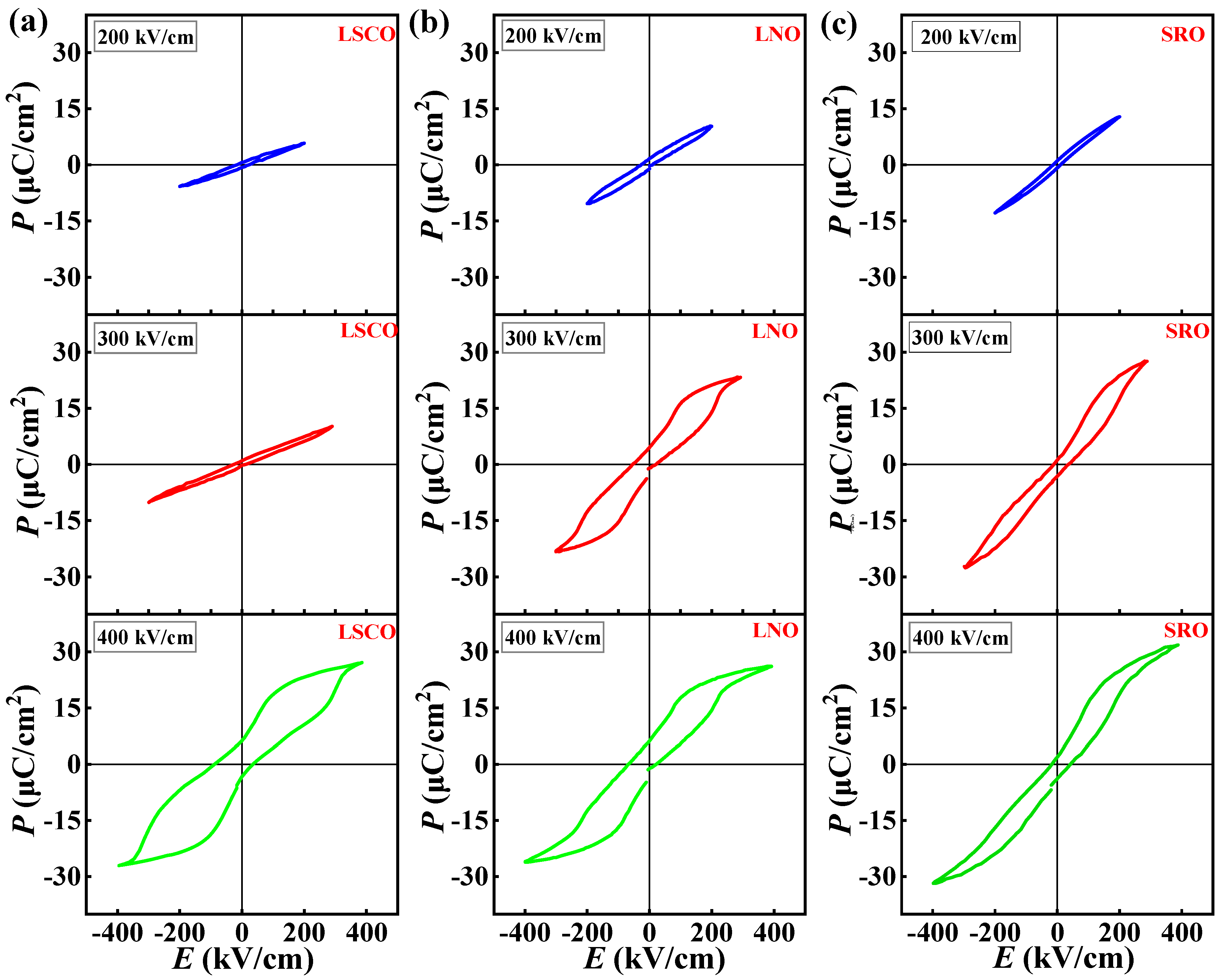
The P-E loops of ANO films grown on LSCO, LNO and SRO bottom electrodes are shown in Figure 5. The applied electric fields are set to be 200 kV/cm, 300 kV/cm and 400 kV/cm. It can be seen that ANO film grown on LSCO bottom electrode shows linear P-E loops at 200–300 kV/cm and double P-E loops at 400 kV/cm. When ANO films are grown on LNO and SRO, bottom electrodes show slim P-E loops at 200 kV/cm and double P-E loops at 300–400 kV/cm. These results indicate that all ANO films are of AFE nature, and the AFE stability of ANO film grown on LSCO bottom electrode is stronger than those grown on LNO and SRO bottom electrodes. More importantly, the ANO films show symmetrical double P-E loops, which are much better than those reported in the literature [15,16]. In Sakurai’s work, the shapes of ANO films prepared by PLD are not very good [15]. And no double P-E loops were observed in AFE ANO films prepared via the chemical solution deposition due to their small Eb [16]. Compared to these reports, our results show some progress. The different AFE stability of ANO films grown on LSCO, LNO and SRO bottom electrodes is attributed to the varied in-phase compressive stress. Detailed properties of the ANO films, including Pr, Pmax, ∆P (∆P = Pmax − Pr), EF, EA, and ΔE (ΔE = EF − EA), are summarized in Table 2. Pmax (Pr) of ANO films grown on LSCO, LNO and SRO bottom electrodes are 27.1 μC/cm2 (6.2 μC/cm2), 26.1 μC/cm2 (6.0 μC/cm2) and 24.0 μC/cm2 (2.9 μC/cm2), respectively. It can be found that the EF decreased from 272 kV/cm to 190 kV/cm by changing the LSCO, LNO and SRO bottom electrodes, and the EF of ANO film grown on SRO bottom electrode is the smallest, indicating that the AFE-FE phase transition occurs more easily in the ANO film grown on SRO bottom electrode than those grown on LSCO and LNO bottom electrodes. This may be due to the fact that the ANO film grown on the SRO bottom electrode is subjected to less in-phase compressive stress, which leads to the weakness of AFE stability.
4. Conclusions
In summary, ANO thin films were deposited by PLD on LSCO, LNO and SRO bottom electrodes and (001) STO substrate, in which the in-plane compressive stress of ANO films was regulated by changing the bottom electrodes from LSCO, LNO to SRO. The effects of bottom electrodes on the dielectric properties and AFE stability of ANO films were studied. It was found that the ANO films grown on LSCO, LNO and SRO bottom electrodes are epitaxial with dense microstructure. With the change of LSCO, LNO to SRO bottom electrode, the out-of-plane lattice constant c of ANO films gradually decreased, implying the weakened in-plane compressive stress in ANO films. The relative dielectric permittivity of ANO films becomes higher by changing the bottom electrodes from LSCO, LNO to SRO. In addition, the EF decreased from 272 kV/cm to 190 kV/cm with varied bottom electrodes, indicating weakened AFE stability, which makes the electric field-induced AFE-FE phase transition easier in ANO films. These results offer a new strategy to regulate and control the AFE stability in ANO materials.
Author Contributions
Investigation, Q.M. and Y.Z.; data curation, Z.D. and S.Z.; writing—original draft preparation, Q.M. and X.L.; writing—review and editing, L.Z.; supervision, S.Z.; project administration, S.Z. and L.Z.; funding acquisition, S.Z. and L.Z. All authors have read and agreed to the published version of the manuscript.
Funding
This work was supported by the Natural Science Foundation of Hebei Province, China (No. E2021201044), the National Natural Science Foundation of China (No.51802068), the State Key Laboratory of New Ceramic and Fine Processing Tsinghua University (No. KF202005), and the Guangdong Basic and Applied Basic Research Foundation (2021A1515110185).
Institutional Review Board Statement
Not applicable.
Informed Consent Statement
Not applicable.
Data Availability Statement
Not applicable.
Conflicts of Interest
The authors declare no conflict of interest.
References
- Zhao, L.; Gao, J.; Liu, Q.; Zhang, S.; Li, J.-F. Silver Niobate Lead-Free Antiferroelectric Ceramics: Enhancing Energy Storage Density by B-Site Doping. ACS Appl. Mater. Interfaces 2018, 10, 819–826. [Google Scholar] [CrossRef] [PubMed]
- Ren, P.; Ren, D.; Sun, L.; Yan, F.; Yang, S.; Zhao, G. Grain size tailoring and enhanced energy storage properties of two-step sintered Nd3+-doped AgNbO3. J. Eur. Ceram. Soc. 2020, 40, 4495–4502. [Google Scholar] [CrossRef]
- Han, K.; Luo, N.; Mao, S.; Zhuo, F.; Liu, L.; Peng, B.; Chen, X.; Hu, C.; Zhou, H.; Wei, Y. Ultrahigh energy-storage density in A-/B-site co-doped AgNbO3 lead-free antiferroelectric ceramics: Insight into the origin of antiferroelectricity. J. Mater. Chem. A 2019, 7, 26293–26301. [Google Scholar] [CrossRef]
- Lu, Z.; Bao, W.; Wang, G.; Sun, S.-K.; Li, L.; Li, J.; Yang, H.; Ji, H.; Feteira, A.; Li, D.; et al. Mechanism of enhanced energy storage density in AgNbO3-based lead-free antiferroelectrics. Nano Energy 2021, 79, 105423. [Google Scholar] [CrossRef]
- Zhang, Y.; Li, X.; Song, J.; Zhang, S.; Wang, J.; Dai, X.; Liu, B.; Dong, G.; Zhao, L. AgNbO3 antiferroelectric film with high energy storage performance. J. Mater. 2021, 7, 1294–1300. [Google Scholar] [CrossRef]
- Ahn, Y.; Seo, J.; Lee, K.J.; Son, J.Y. Ferroelectric domain of epitaxial AgNbO3 thin film. J. Cryst. Growth 2016, 437, 10–13. [Google Scholar] [CrossRef]
- Kania, A. An additional phase transition in silver niobate AgNbO3. Ferroelectrics 1998, 205, 19–28. [Google Scholar] [CrossRef]
- Luo, N.; Han, K.; Liu, L.; Peng, B.; Wang, X.; Hu, C.; Zhou, H.; Feng, Q.; Chen, X.; Wei, Y. Lead-free Ag1-3xLaxNbO3 Antiferroelectric Ceramics with High Energy Storage Density and Efficiency. J. Am. Ceram. Soc. 2019, 102, 4640–4647. [Google Scholar] [CrossRef]
- Luo, N.; Han, K.; Zhuo, F.; Xu, C.; Zhang, G.; Liu, L.; Chen, X.; Hu, C.; Zhou, H.; Wei, Y. Aliovalent A-site engineered AgNbO3 lead-free antiferroelectric ceramics toward superior energy storage density. J. Mater. Chem. A 2019, 7, 14118–14128. [Google Scholar] [CrossRef]
- Zhao, L.; Liu, Q.; Gao, J.; Zhang, S.; Li, J. Lead-Free Antiferroelectric Silver Niobate Tantalate with High Energy Storage Performance. Adv. Mater. 2017, 29, 1701824. [Google Scholar] [CrossRef] [PubMed]
- Fu, D.; Endo, M.; Taniguchi, H.; Taniyama, T.; Itoh, M.; Koshihara, S.-Y. Ferroelectricity of Li-doped silver niobate (Ag, Li)NbO3. J. Phys. Condens. Mat. 2011, 23, 075901. [Google Scholar] [CrossRef] [PubMed] [Green Version]
- Fu, D.; Itoh, M.; Koshihara, S.Y. Dielectric, Ferroelectric, and Piezoelectric Behaviors of AgNbO-KNbO3 Solid Solution. J. Appl. Phys. 2009, 106, 104104. [Google Scholar] [CrossRef]
- Ma, J.; Yan, S.; Xu, C.; Cheng, G.; Mao, C.; Bian, J.; Wang, G. Enhanced energy storage properties of silver niobate ceramics under hydrostatic pressure. Mater. Lett. 2019, 247, 40–43. [Google Scholar] [CrossRef]
- Liu, Z.; Lu, T.; Xue, F.; Nie, H.; Withers, R.; Studer, A.; Kremer, F.; Narayanan, N.; Dong, X.; Yu, D.; et al. Lead-free (Ag, K)NbO3 materials for high-performance explosive energy conversion. Sci. Adv. 2020, 6, eaba0367. [Google Scholar] [CrossRef] [PubMed]
- Sakurai, H.; Yamazoe, S.; Wada, T. Ferroelectric and antiferroelectric properties of AgNbO3 films fabricated on (001), (110), and (111) SrTiO3 substrates by pulsed laser deposition. Appl. Phys. Lett. 2010, 97, 042901. [Google Scholar] [CrossRef]
- Shu, L.; Zhang, X.; Li, W.; Gao, J.; Wang, H.; Huang, Y.; Li, Q.; Liu, L.; Li, J.F. Phase-pure antiferroelectric AgNbO3 films on Si substrates: Chemical solution deposition and phase transitions. J. Mater. Chem. A 2022, 10, 12632–12642. [Google Scholar] [CrossRef]
- Zhu, L.; Wang, X.; Lou, X. Effects of epitaxial strain on antiferrodistortion of AgNbO3 from first-principle calculations. Phys. Status Solidi-R. 2018, 12, 1800007. [Google Scholar] [CrossRef]
- Liang, Y.C.; Liang, Y.C. Fabrication and electrical properties of strain-modulated epitaxial Ba0.5Sr0.5TiO3 thin-film capacitors. J. Electrochem. Soc. 2007, 154, G193–G197. [Google Scholar] [CrossRef]
- Hao, J.H.; Luo, Z.; Gao, J. Effects of substrate on the dielectric and tunable properties of epitaxial SrTiO3 thin films. J. Appl. Phys. 2006, 100, 114107. [Google Scholar] [CrossRef]
Figure 1.
XRD patterns (a) and magnified (002) peaks (b) of ANO films grown on LSCO, LNO and SRO bottom electrodes.
Figure 1.
XRD patterns (a) and magnified (002) peaks (b) of ANO films grown on LSCO, LNO and SRO bottom electrodes.

Figure 2.
Phi scanning of ANO films (a); surface and cross-section SEM images of ANO films grown on SRO (b,e), LNO (c,f) and LSCO (d,g) bottom electrodes.
Figure 2.
Phi scanning of ANO films (a); surface and cross-section SEM images of ANO films grown on SRO (b,e), LNO (c,f) and LSCO (d,g) bottom electrodes.
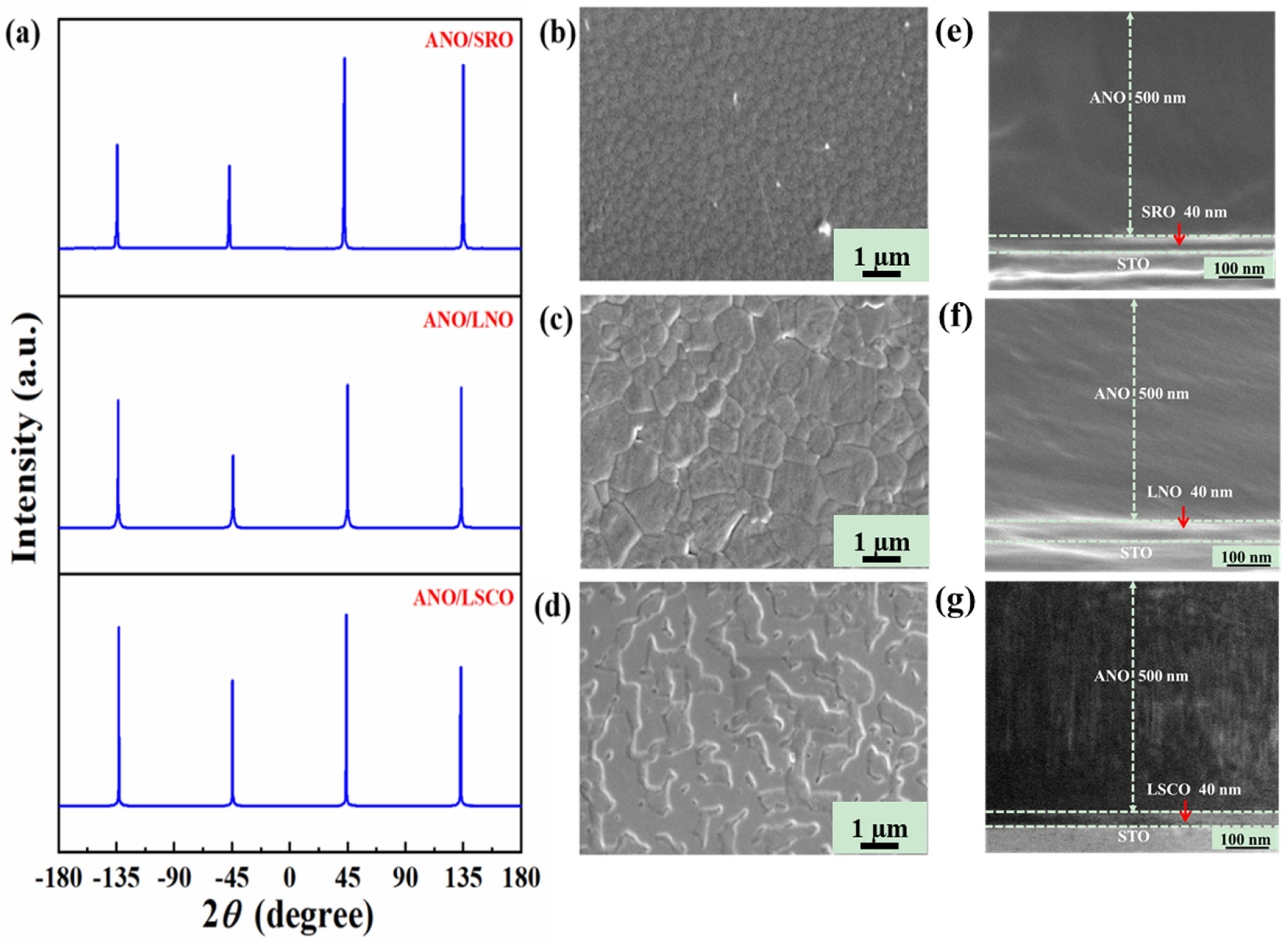
Figure 3.
Frequency stability of relative dielectric permittivity and dielectric loss of ANO films grown on LSCO, LNO and SRO bottom electrodes.
Figure 3.
Frequency stability of relative dielectric permittivity and dielectric loss of ANO films grown on LSCO, LNO and SRO bottom electrodes.
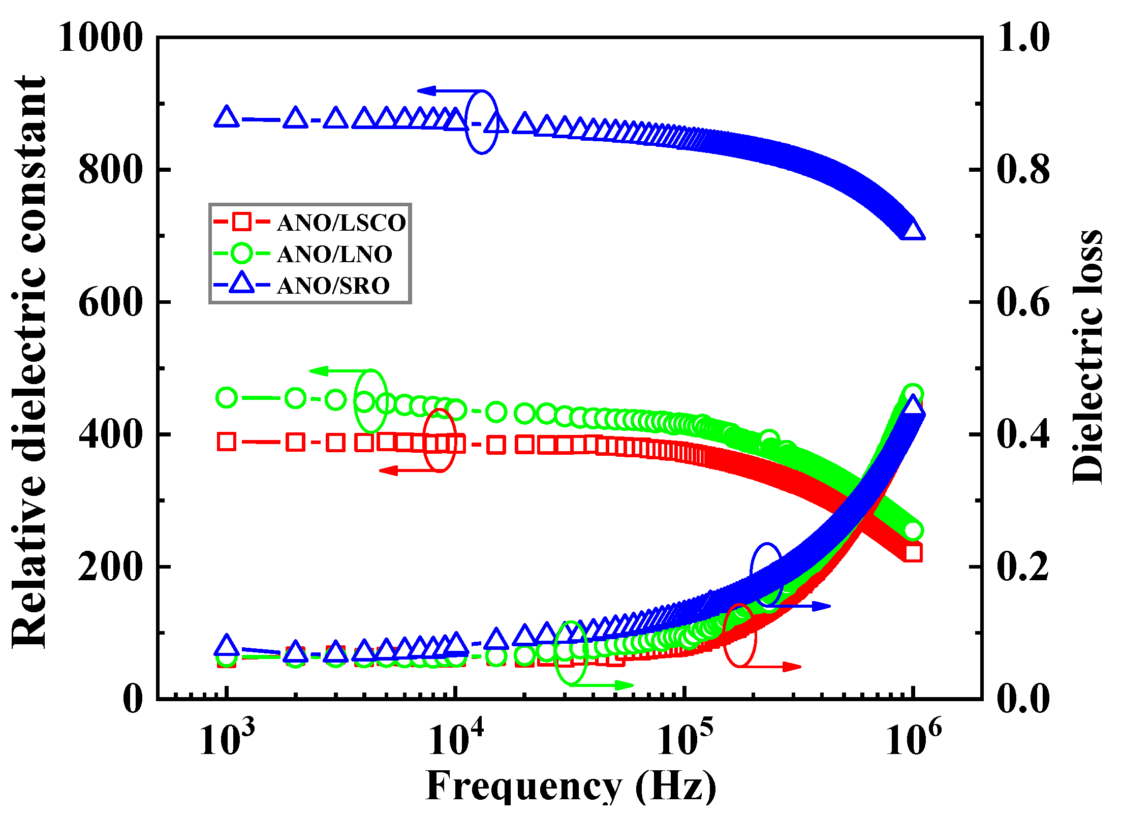
Figure 4.
Leakage current density of ANO films grown on LSCO (a), LNO (b) and SRO (c) bottom electrodes. The insets show the conductive mechanisms of ANO films corresponding to (a–c).
Figure 4.
Leakage current density of ANO films grown on LSCO (a), LNO (b) and SRO (c) bottom electrodes. The insets show the conductive mechanisms of ANO films corresponding to (a–c).
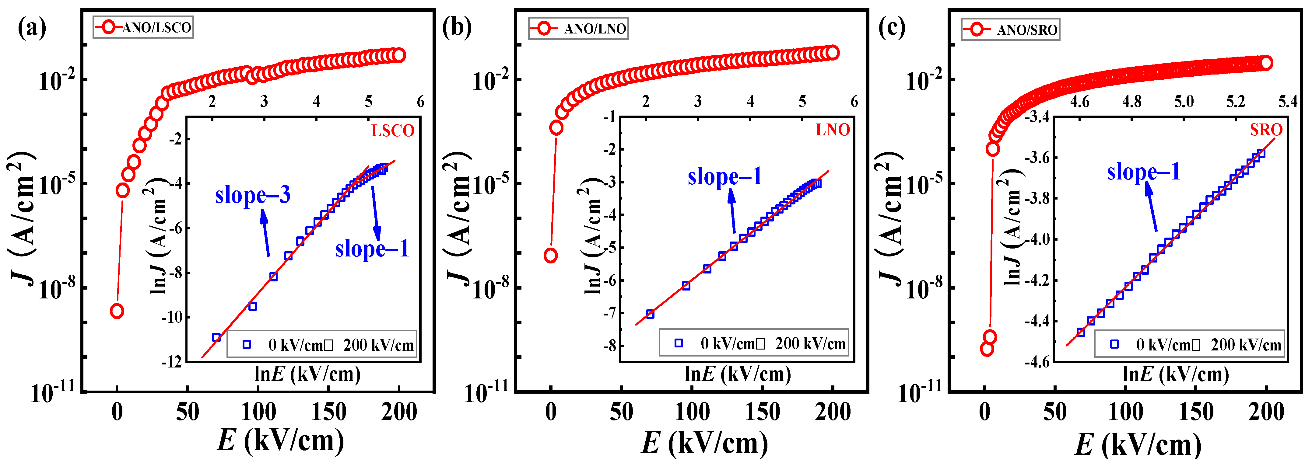
Figure 5.
P-E loops of ANO films grown on LSCO (a), LNO (b) and SRO (c) bottom electrodes under 200 kV/cm, 300 kV/cm and 400 kV/cm.
Figure 5.
P-E loops of ANO films grown on LSCO (a), LNO (b) and SRO (c) bottom electrodes under 200 kV/cm, 300 kV/cm and 400 kV/cm.

Table 1.
Out-of-plane lattice constant c of LSCO, LNO and SRO bottom electrodes and ANO films.
| Bottom Electrodes | Lattice Constant c | |
|---|---|---|
| Bottom Electrodes | ANO Films | |
| LSCO | 3.835 Å | 3.983 Å |
| LNO | 3.849 Å | 3.964 Å |
| SRO | 3.920 Å [15] | 3.949 Å |
Table 2.
Properties of ANO films grown on LSCO, LNO and SRO bottom electrodes.
| Bottom Electrodes | EF (kV/cm) | EA (kV/cm) | Pmax (μC/cm2) | Pr (μC/cm2) | J (A/cm2) |
|---|---|---|---|---|---|
| LSCO | 272 | 20 | 27.1 | 6.2 | <0.050 |
| LNO | 217 | 25 | 26.1 | 6.0 | <0.059 |
| SRO | 190 | 41 | 24.0 | 2.9 | <0.030 |
Publisher’s Note: MDPI stays neutral with regard to jurisdictional claims in published maps and institutional affiliations. |
© 2022 by the authors. Licensee MDPI, Basel, Switzerland. This article is an open access article distributed under the terms and conditions of the Creative Commons Attribution (CC BY) license (https://creativecommons.org/licenses/by/4.0/).
Share and Cite
MDPI and ACS Style
Ma, Q.; Li, X.; Zhang, Y.; Duo, Z.; Zhang, S.; Zhao, L. Dielectric and Antiferroelectric Properties of AgNbO3 Films Deposited on Different Electrodes. Coatings 2022, 12, 1826. https://doi.org/10.3390/coatings12121826
AMA Style
Ma Q, Li X, Zhang Y, Duo Z, Zhang S, Zhao L. Dielectric and Antiferroelectric Properties of AgNbO3 Films Deposited on Different Electrodes. Coatings. 2022; 12(12):1826. https://doi.org/10.3390/coatings12121826
Chicago/Turabian StyleMa, Qingzhu, Xiang Li, Yanle Zhang, Zhijin Duo, Suwei Zhang, and Lei Zhao. 2022. "Dielectric and Antiferroelectric Properties of AgNbO3 Films Deposited on Different Electrodes" Coatings 12, no. 12: 1826. https://doi.org/10.3390/coatings12121826
Note that from the first issue of 2016, this journal uses article numbers instead of page numbers. See further details here.