
Noble Infrared Optical Thickness Monitoring System Based on the Algorithm of Phase-Locked Output Current–Reflectivity Coefficient


1
School of OptoElectronic Engineering, Changchun University of Science and Technology, Changchun 130013, China
2
School of Energy and Power Engineering, Changchun Institute of Technology, Changchun 130103, China
*
Author to whom correspondence should be addressed.
Coatings 2022, 12(6), 782; https://doi.org/10.3390/coatings12060782
Submission received: 27 April 2022
/
Revised: 26 May 2022
/
Accepted: 31 May 2022
/
Published: 6 June 2022
(This article belongs to the Special Issue Optical Thin Films: Preparation, Application and Development)
Abstract
:With the rapid development of modern science and technology, the application of infrared (IR) optical thin films is increasingly widespread, including in aerospace, autonomous driving, military development, and the fight against Coronavirus Disease 2019 (COVID-19), in which thin film devices play an important role. Similarly, with the improvement of user requirements, the precision requirements for the preparation of optical films are also developing and improving. In this paper, the IR optical thickness monitoring system is studied with the noble algorithm introducing the phase-locked amplifier current and single film reflectivity coefficient. An optical control system is developed to monitor the IR thin film accurately, which aids the IR narrow-band filter film research.
1. Introduction
Optical films form the basis of optical components. No matter whether the films are used in lenses, windows, or in special fields such as medical and military, the monitoring accuracy of film thickness is very high. The optical thickness of the film is an important parameter that directly affects the optical properties of the film [1]. The optical monitor system is the part that monitors the optical thickness of the thin film in the vacuum coating machine. Unlike the crystal control system, it does not simply monitor the physical thickness; rather, it determines the extreme point based on the product of the refractive index and the physical thickness, thereby controlling the film thickness. This method can effectively reduce refractive index change due to the influence of temperature, vacuum degree, evaporation rate, and other factors during the evaporation process, making the monitoring accuracy more precise [2].
Modern optical systems have become increasingly complex with harsh application conditions, such as 193 nm lithography. At this wavelength, the materials used are usually SiO2 and CaF2, with refractive indexes of approximately 1.56 and 1.50, respectively. The refractive index is relatively small. To achieve a small scribed linewidth, if a single spherical surface is used, the number of lenses will reach about 30, and even if an aspherical surface is used, about 15 lenses are required [3]. With so many lenses, if they are not coated, according to the Fresnel formula, if the loss of each surface is about 4%, the transmittance of the whole system will be very small, and the light energy will be lost. For the infrared system, due to the large refractive index of the material used, the reflectivity of one side will be large, at more than 10% (the refractive index of the material is great). For a system with only two lenses in the infrared part, the transmittance is approximately 60%. Therefore, modern optical systems must be coated, and each surface must be coated with antireflective film for refractive systems. At the same time, another function of coating the system with the antireflection film is to reduce the stray light in the system. These stray lights usually form ghost images and affect the system’s final output. If an antireflection film is plated on all sides, a high-quality image will be formed on the image surface. If an antireflection film is not plated on the first and third sides, it will form multiple reflections. Finally, a ghost image will be formed in front of the set image, affecting the system’s performance [4,5].
The requirements for optical films have improved, including the increase in the number of films and the improvement of film accuracy. For example, the bandwidth of a narrow-band filter used in optical communication is usually less than 1 nm, and dozens of thin films must be plated. In addition, some band-pass or band-stop optical films with high requirements require only a few nanometers from the pass band to stop band or from the stop band to pass band. At this time, if all the plated optical films adopt a regular film system, multiple layers are required [6]. When plating multilayer films, the crystal control method will result in a jump in the crystal vibration frequency with the increase of the number of layers. This is easily affected by the heat accumulation effect and radiation. In the case of a multilayer coating, if the single film has a small error, the entire film system will fail when a crystal oscillator is used for monitoring. However, when the optical monitor method is used, if the monolayer error occurs, the coating layer can be compensated by coating other layers, which is the main advantage of optical monitoring. In contrast, the optical monitoring monitors the optical thickness of the optical film, while the crystal control monitors the physical thickness of the film, so the optical monitoring is considered to be more direct [7].
Regarding the research and development of optical control systems in the visible light and near-infrared bands, some PVD (physical vapor deposition) device companies can create these systems very effectively, such as Leybold Vacuum in Europe, Shincron and Optorun in Japan, and Jiasen Optoelectronics in China. As for the research and development of optical control systems in the mid-infrared band, only one company from Japan, Optorun, has relatively stable products [8]. In particular, regarding the important role of infrared film in the military, it is urgent to develop a research and development IR optical monitor system. In this paper, a detailed description and analysis is presented from the hardware construction, data acquisition, and signal processing in the early stage to the filtering algorithm and the judgment and stop algorithm in the later stage. Through systematic research, a high-precision wide-spectrum infrared optical film thickness monitoring system was fabricated and installed on a vacuum coating machine produced by Shanghai Mifeng Optoelectronics, and a series of infrared narrow-band filters were prepared [9].
2. Experiment
Figure 1 is the structural block diagram of the IR optical monitor system. It is divided into two parts: the hardware system and software system. In terms of hardware, the blackbody radiation light source (from Thorlabs) is selected as the light-emitting device of the optical monitor system. Sapphire (from Edmund) is an important device for optical fiber conduction. Sr540 (from Stanford) is a chopper device that converts a DC optical signal into an AC optical signal. An IR grating monochromator is used to intercept the monochromatic light required for monitoring. Indium arsenide photodetector (from Zolix) is a detector that can detect a wide band of 3 to 5 microns. The transimpedance amplifier is also an indispensable part of the optical system. NI LabVIEW (20.0) launched by the Ni company was chosen as the programming language for software development [10]. In this system, the stability of the detector has a great impact. Therefore, the temperature controller is introduced to ensure the temperature stability of InGaAs. The specific contents are as follows:
2.1. Construction of the Hardware Part
The hardware part’s construction is shown in Figure 2. The IR optical film thickness monitoring system comprises a light source, chopper, monochromator, IR detector, transimpedance amplifier, and lock-in amplifier. The black-body radiation source emits a beam of light from the light projector, which passes through the chopper and enters the monochromator. The monochromator filters the light into light of a single wavelength, and the infrared detector converts the light signal into an electrical signal and a current signal at the exit end. After the transimpedance amplifier becomes a voltage signal, it is finally amplified and converted into a digital signal by a lock-in amplifier and sent to the PC terminal.
2.2. Construction of the Software Part
The software portion is presented as a block diagram. After detecting that the communication is normal, the parameter setting of the monochromator is executed; if there is any abnormality, an offline abnormal report is sent immediately. Then, the successful detection signal is transmitted; if it fails, it will be sent again until it is completed. Then, the data reception of each layer process file is carried out, and the film layer begins signal reception, which is carried out after the data reception is completed; the signal acquisition is started, the lock-in amplifier range is judged, and the signal is filtered. Regarding curve fitting and extreme value judgment, a single-layer film stop signal is sent after reaching the target film thickness, and it is judged whether to carry out the next layer. If there is another layer, the cycle is entered starting from the process file reception; if there is no next layer, a coating end signal is sent, and finally the coating work ends.
2.3. Savitsky–Golay Smoothing Filter
After the PC end receives the digital signal, it must first perform noise processing. This paper comprehensively compares the mean filtering method, Butterworth filtering method, and low-pass filtering method, and we finally choose the Savitsky–Golay filtering method, which avoids the defects of other methods such as signal distortion and high-frequency signal loss [11,12].
Savitsky–Golay filtering is a combination of neighborhood smoothing filtering and least squares. It performs quadratic or multiple fitting on nl + nR + 1 points, and then takes gi as the multiline or the value at position i. For example, the fitted polynomial degree is M, and the fitted model is a0 + ai + …… + aMiM; there are nl + nR + 1 numbers in it, and the value is fnL, ……fnR. The coefficient a is obtained according to the least-squares method:
where 0 m represents the 0 th row and mth column of the matrix. Figure 3 shows the block diagram of the Savitsky–Golay filtering method implemented by LabVIEW [13]. When using the conventional photoelectrode value method, the ratio of the extreme point and the stopping point is usually used to judge the stop of the film after passing the extreme point [14]. In this paper, according to the substitution of the energy reflectivity formula, the extreme point is reversely fitted through the change of the real-time theoretical curve. The position of the extreme point is judged in advance so that the thin layer, originally less than one-quarter of the optical thickness, can be accurately judged, which greatly improves the accuracy of the thin layer in the film system and also reduces the sensitivity of the film layer to a minimum, making the spectrum of the prepared infrared film more consistent with the designed spectrum.
2.4. Photoelectrode Value Method
According to the theory of wave optics, a light wave is an electromagnetic shear wave. The relationship between the electromagnetic field intensity of a light wave at any position in space and the medium’s performance is established through the Maxwell equation and material equation.
In a medium, the electric field and magnetic field intensity of a light wave can be expressed as
Substituting into Maxwell’s equations and using in the material equation, the relationship between H and E can be obtained:
In addition, intermediate variables are introduced:
where Y is called the optical admittance of the medium, = 1/377S, μ ≈ 1. So,
The physical meaning and constraints of the formula are as follows:
- (1)
- E is the electric field intensity vector, H is the magnetic field intensity vector, B is the magnetic induction intensity vector, is the angular frequency of the plane wave, λ is the wavelength of the electromagnetic wave, r is the coordinate vector, N is the complex refractive index, and l is the extinction coefficient;
- (2)
- E., H, and l0 are perpendicular to each other and conform to the right-handed law—the light wave is an electromagnetic shear wave;
- (3)
According to the theory of wave optics, the amplitude reflection factor and transmission factor of the electromagnetic wave reflected and transmitted at the interface formed by two media are
The following hold according to the boundary condition relationship [16] of an electromagnetic field in electrodynamics theory.
- (1)
- When the electromagnetic wave is vertically incident on an interface, there isandso,
- (2)
- When the electromagnetic wave is obliquely incident on an interface,for a TE wave and s-polarized wave, e is parallel to the interface, soSo,For a TM wave and p-polarized wave incident, h is parallel to the interface, soSo,
If the ratio of the tangential component of the magnetic field intensity and the tangential component of the electric field intensity when the electromagnetic wave is obliquely incident on an interface are regarded as the effective optical admittance when the electromagnetic wave is obliquely incident, there are two different effective optical admittances for the s-polarized wave incident and p-polarized wave incident:
Substituting Equations (21) and (22) into Equations (11), (12), (15) and (16),
For the convenience of calculation, the modified admittance is introduced:
Then, the Fresnel formula can be simplified to
Equations (29) and (30) are used to calculate and , where the in the formula should be carried into , K = 1. Then, and can be calculated. When p, the in the formula should be carried into . According to the theory of wave optics [17], the energy reflectivity and transmittance of the interface formed by the two media to the light wave are
where a is the energy absorption rate for an all-dielectric film system without absorption, .
Therefore, the corresponding optical admittance can be obtained as long as the two media’s refractive index and light incidence angle are known. The reflectivity and refractive index of a single interface can be calculated using Equations (31) and (32) [15,18]. In many calculation methods of optical properties of thin films, the idea of an equivalent interface is the same. A multi-interface thin film system can be regarded as a single interface. The equivalent interface is regarded as the incident mediu“”? m and the equivalent medium [19,20,21]. The refractive index of the incident medium is still . The optical admittance of the equivalent medium is 0. Therefore, the reflectivity of the thin film system is the reflectivity of the equivalent interface, and the reflectivity calculation formula of the equivalent interface is
The corresponding equivalent optical admittance can be used to calculate the reflectivity of any complex thin film system to its equivalent interface. The premise is to establish the relationship between the equivalent optical admittance and the thin film system [22,23].
Firstly, the quantitative relationship between the equivalent optical admittance y of the single-layer dielectric film and substrate and the dielectric film and base structure parameters is found [24]. As shown in Figure 4, the schematic diagram of the equivalent interface is analyzed as follows.
For both sides of the equivalent interface, the equivalent optical admittance y shall meet
where is the unit wave vector perpendicular to the interface and in the same direction as the incident light [21]. According to the boundary condition h of the electromagnetic field , ,
That is, through the boundary conditions of the electromagnetic field, the equivalent optical admittance y is compared with the intensity E of the electromagnetic field in the incident medium , and has established contact. The physical meaning of the four quantities in the formula is as follows: in the same medium with optical admittance y, at any time, the same light wave corresponds to the electric field intensity vector E and magnetic field intensity vector H. Therefore, there is a relationship between the electromagnetic field intensity vectors of light waves propagating in any medium. For example, there is a relationship between the electromagnetic field intensity vectors of light waves propagating in the incident medium [25],
The boundary formula of the electromagnetic field is . The electric field intensity vector E and magnetic field intensity vector h in 0 are not only the vector sum of all-electric field intensities and all magnetic field intensities at the same point and at the same time on both sides of the interface, but also the tangential component of the vector sum. In the actual single-layer dielectric film system, the boundary conditions of the electromagnetic field can also be used to convert and the intensity E of the electromagnetic field in the incident medium and , as well as establishing the equivalent optical admittance y and the structural parameters of the dielectric film and substrate , which show the quantitative relationship between them. Specifically, the electromagnetic fields on both sides of the same interface are connected using the electromagnetic field boundary condition formula. The phase difference associated with electromagnetic field propagation is used to connect the fields at different positions in the same medium [26,27]. In interface 1, there are
On the inner side of interfaces 1 and 2, the relationship between the complex amplitude intensity of two-point electromagnetic fields with different ordinates and the same abscissa is completely governed by the phase difference introduced by their spatial distance:
Written in matrix form,
In interface 2,
Written in matrix form,
Equation (49) can be substituted into (44) to obtain
Combining Formula (35) and , Equation (50) can be simplified as
So
The result is
where is called the effective phase thickness of the film and represents the effective optical thickness of the film.
Equation (54) can be replaced with Equation (33) to obtain the reflectivity calculation formula of the single-layer dielectric film:
After processing by the filtering algorithm, we use the photoelectrode value method to judge and stop the extreme point of the film thickness. The extremum method of monitoring is optical monitoring, which is based on using the beam interference theory to obtain the reflectivity or transmittance curve to monitor the optical film. Since the collected data are an array of the current value and time output by the phase-locked amplifier, it is necessary to introduce a coefficient of current and reflectivity. At the same time, the measured material of the optical control sheet is glass, and the measured reflectivity needs to pass through the positive and negative surfaces of the glass. Therefore, the measured reflectivity also includes the reflectivity of the glass on both sides. Add to the formula to obtain the final fitting formula, as follows:
The conventional monitoring methods are fitted by the least square method in polynomial fitting. In this paper, the data can be fitted by formula fitting according to the deduced formula. This also allows us to interpret the physical meaning of data and improves the accuracy of fitting data, which is a major breakthrough in the research and development of optical control systems [28].
2.5. Design and Fabrication of IR Narrowband Filters
After a series of simulations were completed, a furnace of an IR narrow-band filter film was evaporated on the vacuum coating machine installed with the IR optical monitor system. First, an IR narrow-band filter film was designed using the film system design software OptiLayer. After many times of film system optimization, the design curve shown in Figure 5 was obtained. Ge and SiO choose two commonly used IR materials for evaporation. Ge was evaporated using a single-point crucible electron gun, and SiO was plated by resistance evaporation. Ion beam-assisted deposition was used throughout.
3. Test and Analysis
There are many methods to control film thickness, of which the quartz crystal vibration method and optical thickness control method are the most commonly used. However, for thick infrared optical films, the control effect of the quartz crystal vibration method is poor. The principle is based on the change of vibration frequency caused by the piezoelectric effect of quartz. However, with the increase of film thickness, the variation of vibration frequency with film thickness is no longer linear, resulting in thickness error. Another conventional optical thickness control method is limited to the selection of an infrared light source and the transmission of an optical waveguide. It can only select the near-infrared band control and use the frequency doubling method for indirect operation. On comparing the test curves and design curves of three different control methods, the advantages of the noble control system are clarified.
3.1. Spectral Test
Figure 6 shows the comparison between the test curve and the design curve obtained by evaporation by the crystal control method and ordinary optical control method. As shown in Figure 5, T is the design curve of the IR narrow band filter, and T1 is the test curve. The actual spectrum of the IR narrow-band filter film prepared by IR optical monitoring control described in this paper is basically consistent with the test spectrum. The control accuracy is much higher than that of the crystal oscillator control method and traditional optical control method. Through data analysis and judgment, the monitoring accuracy can reach 0.005%.
3.2. SEM Test
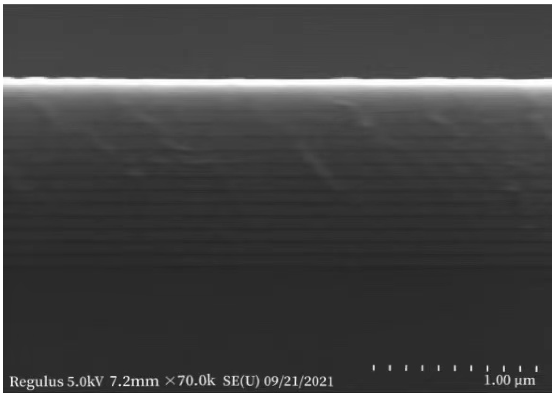
The infrared scanning electron microscope is shown in Figure 7. It can be seen from the figure that the infrared multilayer film evaporated by the optical control system has clear layers and clear boundaries between materials. The physical thickness of the film can be accurately obtained by measuring the cross-section SEM spectrum, and the deviation between the actual thickness and the design thickness is only about 0.5%.
4. Conclusions
In this paper, the expression of the reflectivity of the single-layer film is derived through the principle of optical admittance and the Fresnel formula. According to the signal conversion of the measuring equipment, a new physical quantity is added, and a new fitting formula for the optical control system is obtained. At the same time, the hardware part of the optical control system and the software part of the program are completed, and an optical film thickness monitoring system covering the mid IR band is prepared. On the other hand, the IR narrow-band filter is prepared using the system. The sample meets the requirements of optical parameters and greatly improves the control accuracy. The research and development of the system are of great significance in promoting the development of the military industry and aerospace industries. The research will be further improved to change the scope and accuracy of spectral monitoring in future research.
Author Contributions
Conceptualization, S.D. and X.F.; methodology, S.D.; software, S.D.; validation, X.F., S.D. and C.L.; formal analysis, X.F.; investigation, C.L.; resources, S.D.; data curation, C.L.; writing—original draft preparation, S.D.; writing—review and editing, X.F.; visualization, S.D.; supervision, C.L.; project administration, S.D.; funding acquisition, C.L. All authors have read and agreed to the published version of the manuscript.
Funding
This research received no external funding.
Institutional Review Board Statement
Not applicable.
Informed Consent Statement
Not applicable.
Data Availability Statement
The data used in this research is available from the corresponding author upon reasonable request.
Conflicts of Interest
The authors declare no conflict of interest.
Abbreviations
| List of symbols | |
| E | Electric field intensity vector |
| H | Magnetic field intensity vector |
| B | Magnetic induction intensity vector |
| ω | Angular frequency of plane wave |
| λ | Wavelength of electromagnetic wave |
| r | Coordinate vector |
| N | Complex refractive index |
| k | Extinction coefficient |
| Abbreviations | |
| IR | Infrared |
| COVID-19 | Coronavirus Disease 2019 |
| PVD | Physical vapor deposition |
References
- Ristau, D.; Ehlers, H.; Schlichting, S.; Lappschies, M. State of the art in deterministic production of optical thin films. Proc. SPIE Adv. Opt. Thin Film. III 2008, 7101, 71010C. [Google Scholar]
- Dobrowolski, J.A. Optical properties of films and coatings. In Handbook of Optics; McGraw-Hill: New York, NY, USA, 2010; Chapter IV; pp. 7.15–7.53. [Google Scholar]
- Macleod, H.A. Thin-Film Optical Filters, 4th ed.; CRC Press: Boca Raton, FL, USA; Taylor & Francis: Abingdon, UK, 2010. [Google Scholar]
- Thoeni, W. Deposition of optical coatings: Process control and automation. Thin Solid Film. 1982, 88, 385–397. [Google Scholar] [CrossRef]
- Wilbrandt, S.; Kaiser, N.; Stenzel, O. In-situ broadband monitoring of heterogeneous optical coatings. Thin Solid Film. 2006, 502, 153–157. [Google Scholar] [CrossRef]
- Ristau, D. Characterization and monitoring. In Optical Interference Coatings; Springer: Berlin/Heidelberg, Germany, 2003; pp. 181–205. [Google Scholar]
- Tikhonravov, A.V.; Trubetskov, M.K.; Amotchkina, T.V. Statistical approach to choosing a strategy of monochromatic monitoring of optical coating production. Appl. Opt. 2006, 45, 7863–7870. [Google Scholar] [CrossRef] [PubMed]
- Tikhonravov, A.V.; Trubetskov, M.K. Elimination of cumulative effect of thickness errors in monochromatic monitoring of optical coating production: Theory. Appl. Opt. 2007, 46, 2084–2090. [Google Scholar] [CrossRef] [PubMed]
- van der Laan, C.J. Optical monitoring of nonquarterwave stacks. Appl. Opt. 1986, 25, 753–760. [Google Scholar] [CrossRef]
- Tikhonravov, A.V.; Trubetskov, M.; Amotchkina, T.V. Computational experiments on optical coating production using monochromatic monitoring strategy aimed at eliminating a cumulative effect of thickness errors. Appl. Opt. 2007, 46, 6936–6944. [Google Scholar] [CrossRef]
- Zhao, F. Monitoring of periodic multilayers by the level method. Appl. Opt. 1985, 24, 3339–3342. [Google Scholar] [CrossRef] [PubMed]
- Willey, R.R.; Machado, D.E. Variation of band-edge position with errors in the monitoring of layer termination level for long- and short-wave pass filters. Appl. Opt. 1999, 38, 5447–5451. [Google Scholar] [CrossRef]
- Sullivan, B.T.; Dobrowolski, J.A. Deposition error compensation for optical multilayer coatings I Theoretical description. Appl. Opt. 1992, 31, 3821–3835. [Google Scholar] [CrossRef] [PubMed]
- Lee, C.-C.; Wu, K.; Kuo, C.-C.; Chen, S.-H. Improvement of the optical coating process by cutting layers with sensitive monitoring wavelengths. Opt. Express 2005, 13, 4854–4861. [Google Scholar] [CrossRef] [PubMed]
- Badoil, B.; Lemarchand, F.; Cathelinaud, M.; Lequime, M. Interest of broadband optical monitoring for thin-film filter manufacturing. Appl. Opt. 2007, 46, 4294–4303. [Google Scholar] [CrossRef] [PubMed]
- Tikhonravov, A.; Trubetskov, M.; Amotchkina, T. Optical monitoring strategies for optical coating manufacturing. In Electronic and Optical Materials; Woodhead Publishing: Sawston, UK, 2013; pp. 62–93. [Google Scholar]
- Ristau, D.; Ehlers, H.; Gross, T.; Lappschies, M. Optical broadband monitoring of conventional and ion processes. Appl. Opt. 2006, 45, 1495–1501. [Google Scholar] [CrossRef]
- Wilbrandt, S.; Stenzel, O.; Kaiser, N.; Trubetskov, M.K.; Tikhonravov, A.V. In situ optical characterization and reengineering of interference coatings. Appl. Opt. 2008, 47, C49–C54. [Google Scholar] [CrossRef]
- Waldner, S.; Benz, R.; Biedermann, P.; Jaunzens, A. Broadband optical monitoring combined with additional rate measurement for accurate and robust coating processes. In Optical Interference Coatings; Optical Society of America: Washington, DC, USA, 2010; paper TuC10. [Google Scholar]
- Zöller, A.; Boos, M.; Hagedorn, H.; Klug, W.; Schmidt, C. High accurate in-situ optical thickness monitoring. In Optical Interference Coatings; Optical Society of America: Washington, DC, USA, 2004. [Google Scholar]
- Holm, C. Optical thin film production with continuous reoptimization of layer thicknesses. Appl. Opt. 1979, 18, 1978–1982. [Google Scholar] [CrossRef]
- Zöller, A.; Boos, M.; Hagedorn, H.; Romanov, B. Computer simulation of coating processes with monochromatic monitoring. Proc. SPIE Adv. Opt. Thin Film. III 2008, 7101, 71010G. [Google Scholar]
- Gilo, M.; Cohen, D. Comparison of broad-band and single wavelength monitoring for IR coatings. In Optical Interference Coatings; Optical Society of America: Washington, DC, USA, 2013. [Google Scholar]
- Zöller, A.; Boos, M.; Götzelmann, R.; Hagedorn, H.; Klug, W. Substantial progress in optical monitoring by intermittent measurement technique. Proc. SPIE Adv. Opt. Thin Film. II 2005, 59630, 59630D. [Google Scholar]
- Tikhonravov, A.V.; Trubetskov, M.K.; Amotchkina, T.V.; Pervak, V. Estimations of production yields for selection of a practical optimal optical coating design. Appl. Opt. 2011, 50, C141–C147. [Google Scholar] [CrossRef]
- Chun, B.J.; Hwangbo, C.K.; Kim, J.S. Optical monitoring of nonquarterwave layers of dielectric multilayer filters using optical admittance. Opt. Express 2006, 14, 2473–2480. [Google Scholar] [CrossRef]
- Amotchkina, T.V.; Schlichting, S.; Ehlers, H.; Trubetskov, M.K.; Tikhonravov, A.V.; Ristau, D. Computational manufacturing as a key element in the design-production chain for modern multilayer coatings. Appl. Opt. 2012, 51, 7604–7615. [Google Scholar] [CrossRef]
- Friedrich, K.; Wilbrandt, S.; Stenzel, O.; Kaiser, N.; Hoffmann, K.H. Computational manufacturing of optical interference coatings: Method, simulation results, and comparison with experiment. Appl. Opt. 2010, 49, 3150–3162. [Google Scholar] [CrossRef] [PubMed]
Figure 1.
(a). Structure block diagram of infrared optical monitor control system hardware. (b). Structure block diagram of infrared optical monitor control system software.
Figure 1.
(a). Structure block diagram of infrared optical monitor control system hardware. (b). Structure block diagram of infrared optical monitor control system software.

Figure 2.
Schematic diagram of the hardware structure of the infrared optical monitor system.
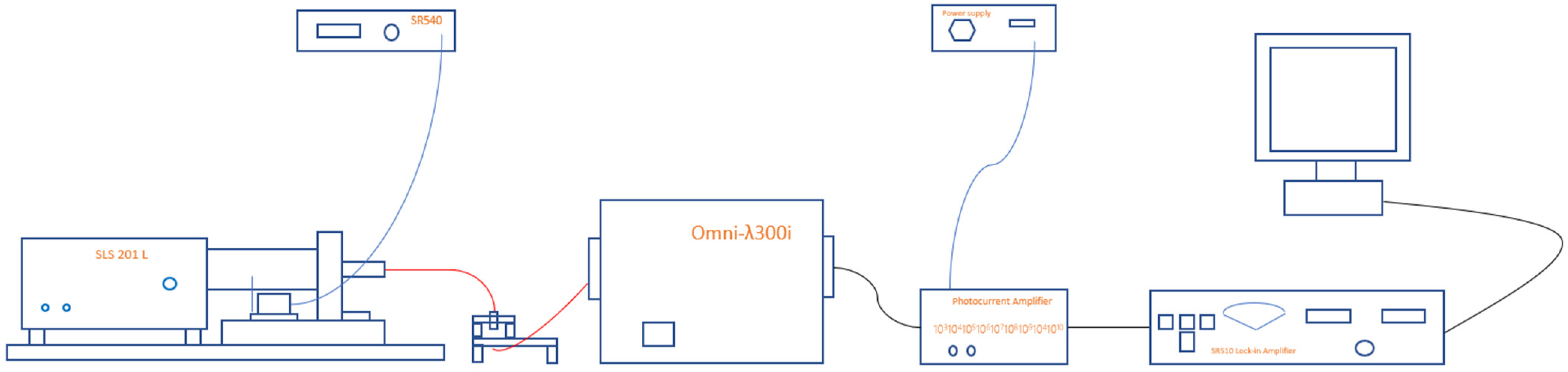
Figure 3.
Implementation of Savitsky–Golay filtering algorithm in Labview.

Figure 4.
Schematic diagram of the equivalent interface.
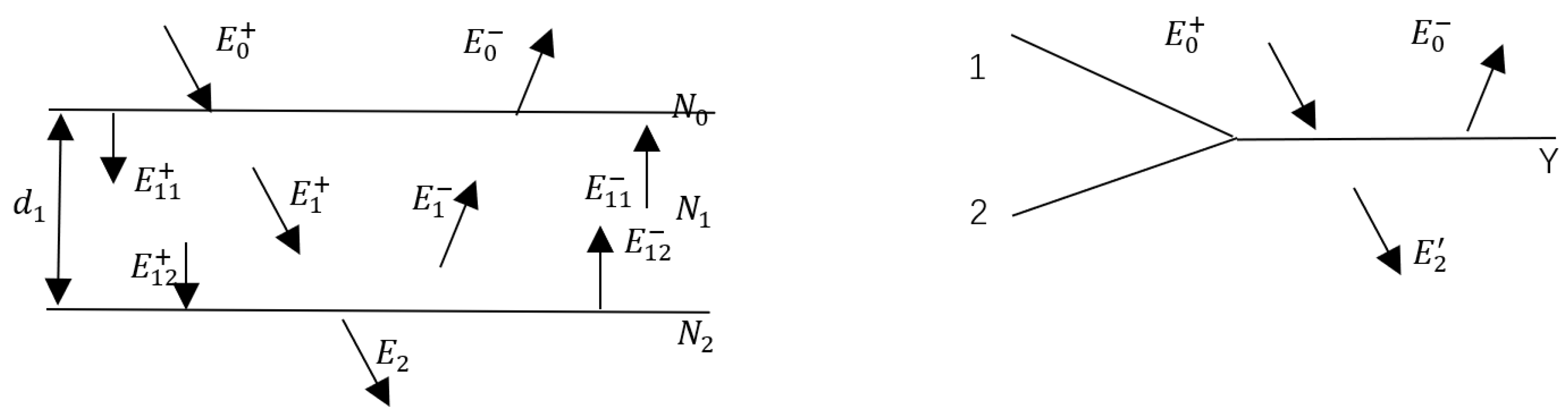
Figure 5.
Comparison of design curve and test curve based on the Noble IR optical monitor.
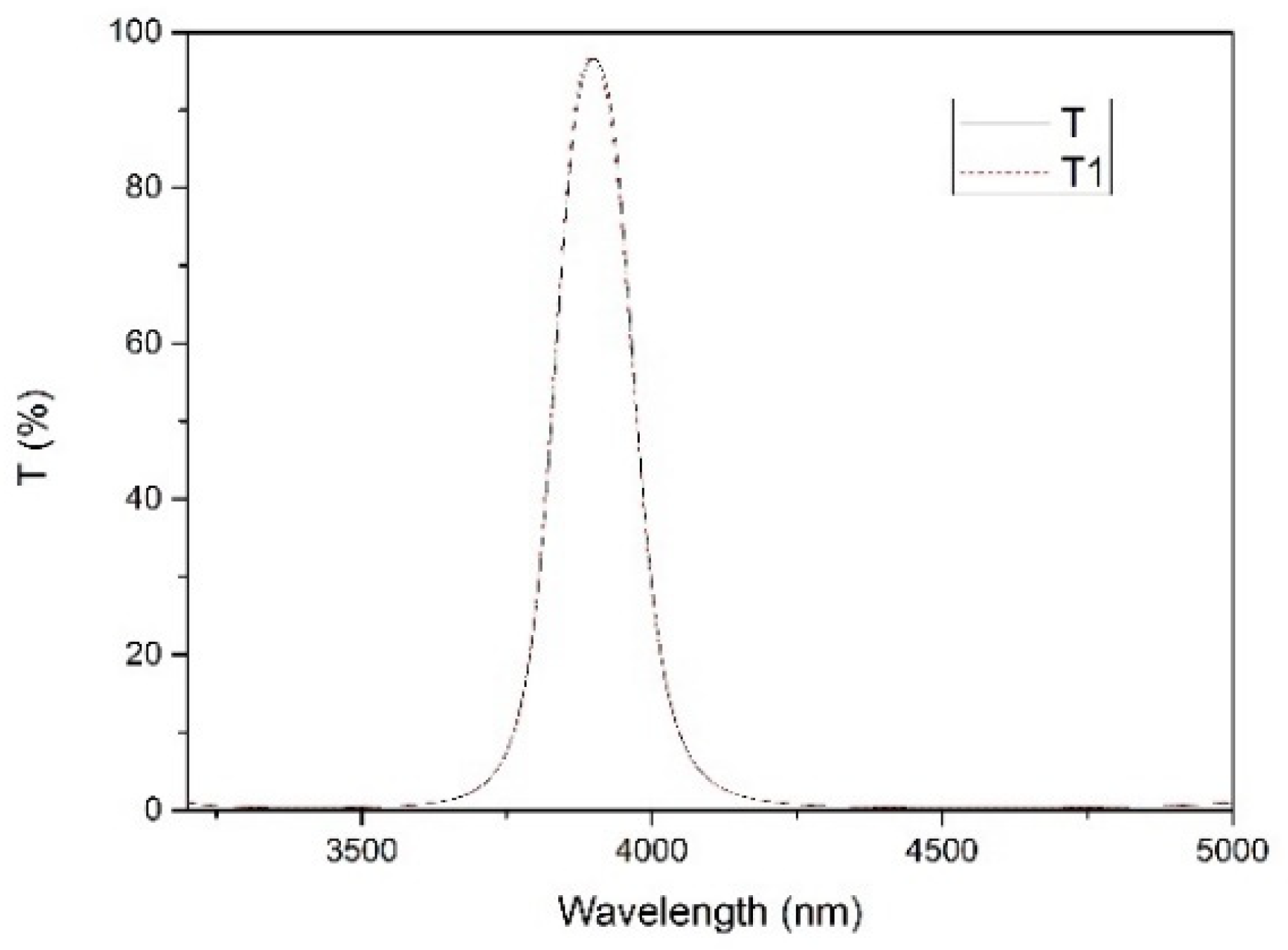
Figure 6.
Comparison of design curve and test curve based on general optical monitor (T2) and crystal monitor system (T3).
Figure 6.
Comparison of design curve and test curve based on general optical monitor (T2) and crystal monitor system (T3).

Figure 7.
Multilayer thin-film SEM spectroscopy.
Publisher’s Note: MDPI stays neutral with regard to jurisdictional claims in published maps and institutional affiliations. |
© 2022 by the authors. Licensee MDPI, Basel, Switzerland. This article is an open access article distributed under the terms and conditions of the Creative Commons Attribution (CC BY) license (https://creativecommons.org/licenses/by/4.0/).
Share and Cite
MDPI and ACS Style
Dong, S.; Fu, X.; Li, C. Noble Infrared Optical Thickness Monitoring System Based on the Algorithm of Phase-Locked Output Current–Reflectivity Coefficient. Coatings 2022, 12, 782. https://doi.org/10.3390/coatings12060782
AMA Style
Dong S, Fu X, Li C. Noble Infrared Optical Thickness Monitoring System Based on the Algorithm of Phase-Locked Output Current–Reflectivity Coefficient. Coatings. 2022; 12(6):782. https://doi.org/10.3390/coatings12060782
Chicago/Turabian StyleDong, Suotao, Xiuhua Fu, and Cheng Li. 2022. "Noble Infrared Optical Thickness Monitoring System Based on the Algorithm of Phase-Locked Output Current–Reflectivity Coefficient" Coatings 12, no. 6: 782. https://doi.org/10.3390/coatings12060782
Note that from the first issue of 2016, this journal uses article numbers instead of page numbers. See further details here.