Article

Synthesis and Characterization of a Zirconium (Zr) Thin Film on Si(100) via Pulsed Laser Deposition

1
Department of Physics & Astronomy, Western Kentucky University, Bowling Green, KY 42101, USA
2
Department of Mathematics, Western Kentucky University, Bowling Green, KY 42101, USA
3
Universities Space Research Association, NASA Marshall Space Center, Huntsville, AL 35805, USA
*
Author to whom correspondence should be addressed.
Coatings 2023, 13(10), 1748; https://doi.org/10.3390/coatings13101748
Submission received: 30 August 2023 / Revised: 3 October 2023 / Accepted: 4 October 2023 / Published: 10 October 2023

Abstract

:
Zirconium (Zr) thin films were deposited on silicon using pulsed laser deposition (PLD) with two laser wavelengths (1064 nm and 532 nm) and varying substrate temperatures (25 °C, 300 °C, and 500 °C) and laser fluences (0.25, 0.5, 1.0 J/cm2). Results indicate that smoother films were obtained with 1064 nm and surface roughness increased with higher fluences. Optimal crystalline films were obtained at 300 °C. XRD, SEM, and AFM analysis revealed distinct patterns and peaks related to laser parameters. The growth mechanisms of a Zr film were computed based on a well-known continuum model of thin film growth. Our simulations agree with experimental observations. The study highlights crucial factors affecting Zr thin film deposition and provides insights for optimizing PLD parameters to achieve high-quality films.

1. Introduction

Zirconium is a highly active transition metal that closely resembles titanium and hafnium and has a strong resistance to corrosion and heat [1]. Additionally, its thin layer of oxide forms an exceptional resistance to acid, alkalis, and seawater. Zirconium occurs naturally in about 30 mineral species, mostly as a silicate in zircon, the oxide baddeleyite and other oxide compounds. Due to its high resistance to corrosion, zirconium is widely used in the manufacture of pumps, valves, and heat exchangers [2]. Zirconium is also used as an alloying agent in the production of some magnesium alloys and as an additive in the manufacture of some steels.
Zirconium is also a material that can be considered for multilayer coating applications. Aluminum-based mirrors have recently been widely investigated in reflective multilayer coatings in extreme ultraviolet spectral regions due to having an L-edge near 17 nm. In particular, Al-based multilayers have potential applications in the construction of mirrors for instruments to detect solar coronal or transition-region emission lines in the wavelength region of 17–19 nm.
It is known that aluminum can be a stable spacer in multilayer combinations. However, inhomogeneous crystallization and interdiffusion between layers, the presence of an oxide layer, and other contamination risks pose serious problems. Among those combinations, Al/Zr multilayers have shown very promising performance in the EUV region. Given its importance in the reflective mirror coatings, the mechanism of the zirconium growth and its characterization are of utmost importance.
There are limited studies regarding the thin film deposition of pure Zr. Romanov et al. compared the electrical properties of Zr thin films deposited on 6H-SiC substrates using pulsed laser deposition with other metals at a substrate temperature of 300 K [3]. Their results indicated that while Zr exhibited slightly worse electrical properties compared to tungsten and gold, it formed a barrier with sufficient ohmic properties for current flow processes.
An additional study was conducted by Fankhauser et al., where epitaxial Zr(0001) thin films were grown on Al2O3(0001) substrates using DC magnetron sputtering at a substrate temperature of 700 °C [4]. The presence of an interfacial layer was observed, and its formation mechanism was investigated. The structural characterization confirmed the epitaxial nature of the film and provided insights into the lattice parameters and orientation relationships between the film and the substrate.
Among the different deposition methods, the pulsed laser deposition (PLD) technique is considered a highly versatile technique for a growing number of thin film applications [5,6,7,8,9,10,11,12]. PLD uses high-energy laser pulses to vaporize the surface of a solid target inside a vacuum chamber and condenses the vapor on a substrate to form a film.
Several factors, including substrate temperature, laser energy density, and oxygen partial pressure, can regulate thermally activated processes. Such processes can include adsorption, desorption, surface diffusion, nucleation, crystallization/recrystallization, substrate surface roughness, and the deposited thin film morphology of Zr. Additional factors such as target-to-substrate distance, repetition rate, and post-growth annealing may also alter the properties of the produced Zr thin films in pulsed laser deposition.
The average size of the nanoparticle and the root mean square roughness were shown to increase with laser fluence when zirconium was deposited on silicon by PLD using an excimer laser with a 248 nm wavelength [13]. The effects of pulse repetition rates on the surface morphologies, specular reflectivity, and resistivity properties of Zr films and Zr deuteride films were investigated to find suitable process parameters for the fabrication of high-quality films for nuclear fusion. The deposited Zr thin films had exceedingly smooth surfaces and high specular reflectivity. Additionally, some depressions were formed in the film when they were exposed to a deuterium atmosphere.
Zirconium thin films deposited on high carbon steel substrates via RF magnetron sputtering have also been analyzed [14]. The annealing process was conducted at temperatures ranging from 600 °C to 1100 °C and was found to promote the diffusion of carbon atoms, resulting in a transformation to zirconium carbide. The samples annealed at 900 °C exhibited the best mechanical properties.
In this work, we performed a series of experiments to understand the effect of deposition parameters of zirconium on Si(100) using a 1064 nm Nd:YAG laser and its second harmonic, especially the laser wavelength, fluence, and substrate temperature. Our study showed that PLD is a viable option for obtaining crystalline zirconium at different substrate temperatures, fluences, and wavelengths.

2. Experimental Setup

A pulsed laser deposition (PLD) system was used to deposit zirconium thin films on Si substrates at various temperature conditions, wavelengths, and fluences. The main components of the equipment set were a pulsed Nd: YAG nanosecond laser source (Continuum Surelite II), a stainless steel ultrahigh vacuum chamber equipped with a substrate holder, and a rotating target holder system. The laser has a fundamental wavelength of 1064 nm, pulse width of 5 nanosecond, 10 Hz repetition rate, and a Gaussian pulse shape with a 6 mm diameter unfocused beam. The second harmonic beam with a 532 nm wavelength was generated using a KDP crystal. The purity of the Zr target was 99.95% and the UHV chamber was pumped down to low 10−7 Torr. The target was rotated at 8 rpm to minimize the particulate formation and the target to substrate distance was around 5 cm.
The surface morphology and cross-sectional thickness of the thin films were investigated by using scanning electron microscopy (SEM, Jeol 6510LV, Tokyo, Japan) and atomic force microscopy (AFM, Nanosurf FlexAFM, Liestal, Switzerland). X-ray diffraction (XRD, Bruker, Karlsruhe, Germany) measurements were performed by using a BRUKER 2nd generation D2 PHASER.
The silicon (100) substrates (MTI Corporation, Richmond, CA, USA) were located 4 cm away from the target vertically. They were ultrasonically cleaned for 5 min after bathing in methanol and storing in deionized water before loading onto the sample holder for deposition. It should be noted that silicon also has a natural oxide layer. The UHV chamber was pumped down to base pressure 10−8 Torr using mechanical rotary, turbomolecular, and ion-sputtering pumps.

3. Results and Discussions

3.1. Effect of Fluence and Wavelength
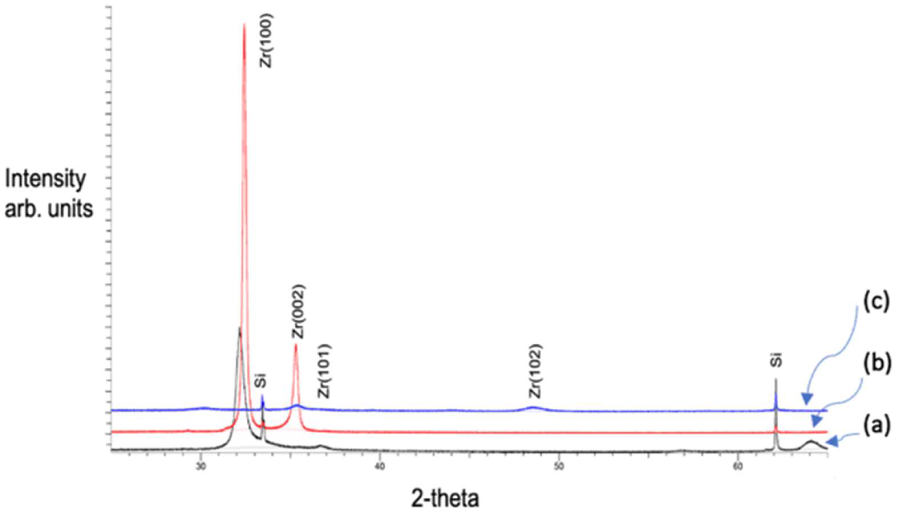
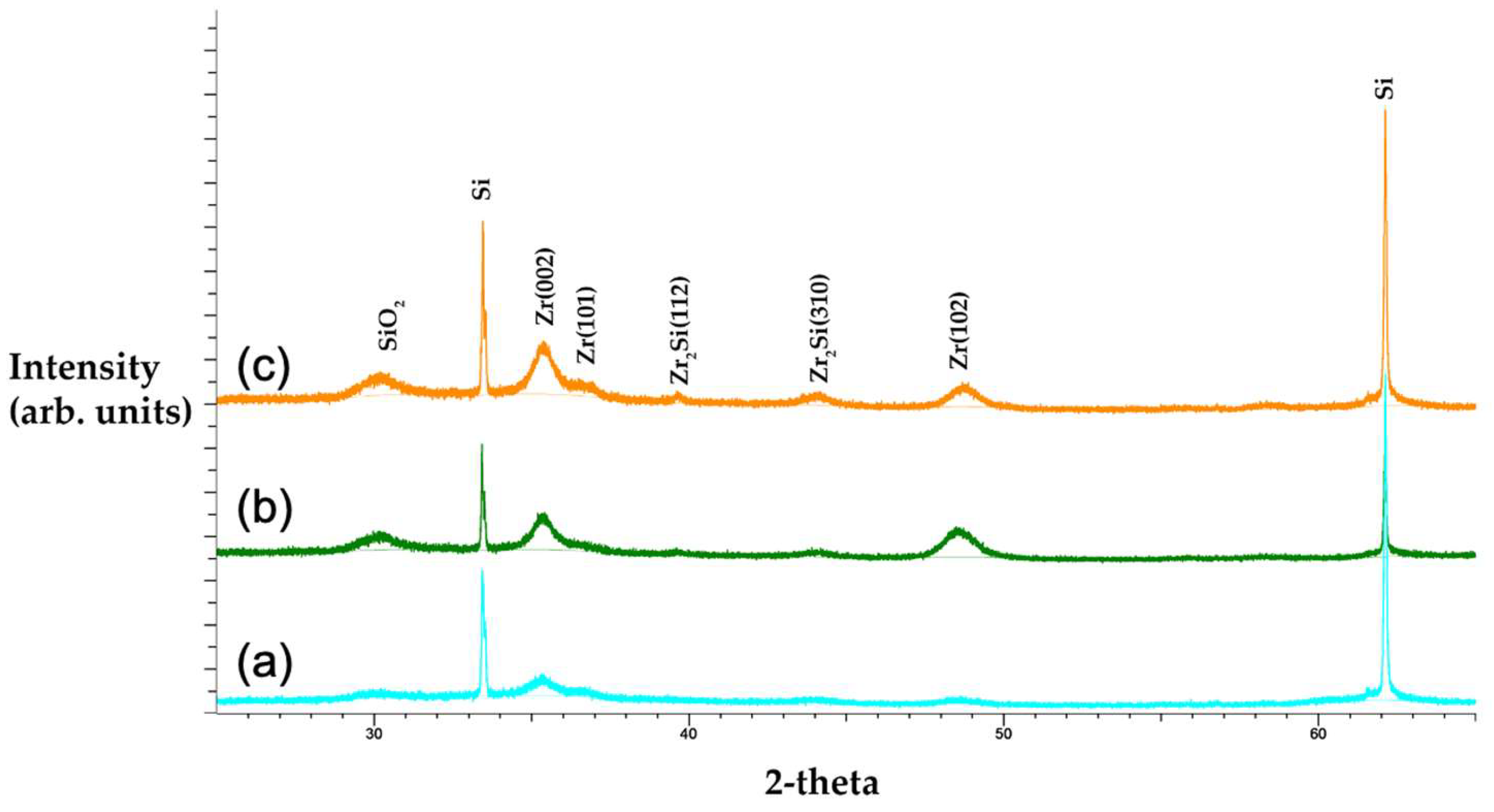
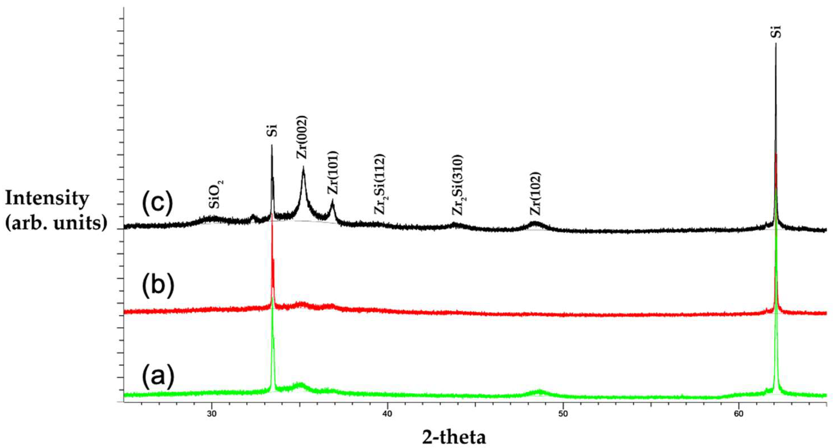
3.1.1. XRD Analysis

At ambient conditions, zirconium crystallizes in a hexagonal close-packed (hcp) structure known as the phase, and the phase transition from α-Zr to (body centered cubic) β-Zr at atmospheric pressure occurs at 1135 K.
The XRD patterns (Database#: COD 1512554 for zirconium) shown in Figure 1 display the intensity of Zr peaks in four different two-theta angles corresponding to Zr (100), Zr (002), Zr (101), and Zr (102) when deposition was carried out with different laser energy densities at a 532 nm wavelength and 500 °C substrate temperature.
The XRD measurements show peaks corresponding to the hexagonal structure of Zr. The obtained peaks corresponded to Miller indices of (100), (002), (101), and (102), in addition to two peaks which belonged to the Si substrate. Figure 1 illustrates XRD data for Zr films obtained using a wavelength of 532 nm at 500 °C using three different fluences. For all three fluences, Zr (100) was not present. A similarly distinct pattern was observed for Zr (002) and Zr (101), where the intensity of the peaks initially increased as the fluence was quadrupled, but there was no visible change in XRD pattern when the laser energy density was doubled. However, peaks became more prominent, and some additional peaks started to appear when the laser energy density was further increased to 1.06 J/cm2. The intensity of Zr (102) first increased with the doubling of the fluence but remained the same with further fluence increases. The laser fluence and wavelength are critical when determining the structure of the deposited films. We previously found that the laser fluence had a significant influence on NbNx film properties such as crystallite size [15]. Laser fluence and wavelength were also shown to affect the structural and optical properties of CuxS films grown with PLD [16].
The ablation rates and film thicknesses were significantly influenced by the laser fluence. A minimum laser fluence that surpassed the material-dependent threshold was necessary for film formation. When using fluences slightly above the ablation threshold, a phenomenon called dissimilar ablation may occur, particularly in multielement materials [17], and when the fluence is just below the threshold laser-induced periodic surface structures can be formed [18,19,20,21]. This refers to the preferential ablation of certain elements. For instance, in the case of SrTiO3, increasing the laser fluence leads to the preferential ablation of Ti, resulting in Ti-rich film growth at higher fluences [22]. Similar effects have been observed in other materials, such as LiCoO2 [23]. In other cases, stoichiometric films are only obtained at fluences significantly higher than the ablation threshold, as seen in BaTiO3 [24]. Using fluences slightly above the ablation threshold can lead to preferential ablation, thereby resulting in low ablation rates and consequently slow deposition rates. This regime is highly sensitive to changes in fluence and it is strongly advised to avoid it in PLD when aiming for reproducible outcomes [25].
Beyond the approximate threshold value of 0.5 J/cm2, increasing the laser fluence exhibited an almost logarithmic growth in the ablation rate. The control of the laser fluence not only governed the rate of deposition but also influenced the kinetic energy of the ablated species. Even at fluences around 1 J/cm2, the maximum kinetic energies exceeded 200 eV. The kinetic energy continued to rise as the fluence increased, reaching up to 900 eV at the maximum tested fluence of approximately 5 J/cm2 [17].
The kinetic energies of the ablated species directly influenced the crystallinity of the resulting film, often by enhancing the adatom mobility. However, it should be noted that kinetic energies above a certain threshold could have adverse effects. For example, kinetic energies exceeding a certain threshold can lead to a significant increase in sputtering yield, Y, which is defined as the ratio of the number of atoms lost from a surface to the number of incident energetic particles striking the surface. Additionally, these highly energetic species can introduce undesired structural formations into the deposited film and cause preferential sputtering, resulting in compositional deviations [26].
Our study shows that the microstructure and surface properties and crystalline structure of zirconium films can be adjusted with laser fluence and wavelength. We report on the effect of the laser fluence on the properties of pulsed lased deposited NbNx films.
Zirconium was then deposited at 1064 nm to study the effect of the wavelength at the same fluences. Figure 2 shows XRD data for the Zr thin films obtained using a 1064 nm wavelength at 500 °C. At the 0.26 J/cm2 fluence, the Zr (100) peak was not visible; however, as the fluence increased to 1.04 J/cm2 it becomes more apparent. In addition, we observed one SiO2 peak at 500 °C. A similarly distinct pattern was observed for Zr (002) and Zr (101), where the intensity of the peaks initially increased as the fluence was quadrupled, but there was no visible change when the fluence was doubled. The intensity of Zr (102) first decreased with the doubling of the fluence but increased again with a further increase in the fluence of 1.06 J/cm2.
Comparing the XRD data of two wavelengths at a substrate temperature of 500 °C and fluences of 0.26 J/cm2 and 0.52 J/cm2, the Zr thin film using 532 nm is shown to be more crystalline as its normalized full width at half-maximum (FWHM) was smaller. However, this reversed for 1.04 J/cm2, as the normalized FWHM for 1064 nm became smaller. In addition, Zr (002) peaks were observed in all three fluences with 532 nm, while they were only observed with 1.06 J/cm2 at 1064 nm.
While multiple synthesis conditions influence the ablation process, one of the most significant conditions is the wavelength of the laser pulse. When the wavelength is shorter, the photon energies increase, allowing for bond breakage within the atomic lattice, thereby resulting in ionization [27]. This leads to the ejection of atoms and ions without adverse heating effects. Shorter wavelengths also result in shallower laser penetration depths and, consequently, lower the threshold fluences and ablation rates. In contrast, longer wavelengths often yield higher densities and larger sizes of particulates and/or droplets. Infrared or visible laser light usually processes materials by producing intense local heating that can melt or vaporize the material, which may cause serious damage to surrounding areas. This contributes to stronger compositional deviations in a film [28]. Therefore, UV irradiation at shorter wavelengths typically yields lower amounts of nano/microparticles as compared to irradiation at longer wavelengths.
During the ablation process, micro- to nanostructures are frequently formed on the surface of the target material. These structures increase the surface area and, in turn, reduce the effective laser fluence. It has been reported that the wavelength of the laser pulse affects the size and frequency of the periodic structures that appear on the target surface [29]. Moreover, the wavelengths not only impact the absorption by the target material, but also influence the absorption by the laser-generated plasma plume [28,30].
The useful range of laser wavelengths for ablation typically falls between 200 and 400 nm. Excimer lasers are often preferred for ablation due to their higher energies and relatively flat top energy profile. In contrast, Nd:YAG lasers demonstrate a Gaussian energy profile. Therefore, the variation in fluence inherent to the Gaussian profile must be considered when determining deposition parameters if using a Nd:YAG laser [17].
It has previously been shown that Zirconium silicide was formed at the interface between the silicon (Si) substrate and Zr films when zirconium was deposited onto the silicon surface with an excimer laser [31]. We have observed similar peaks at 41 and 44 and assigned their values. It should be noted that we have not observed those peaks below 500 °C, which is in agreement with the literature. This could be due to zirconium silicide being too thin or the amorphous nature of the interface. It is known that at high temperatures, atoms’ hopping rates increase and interface reactions occur more easily compared to at low temperatures.

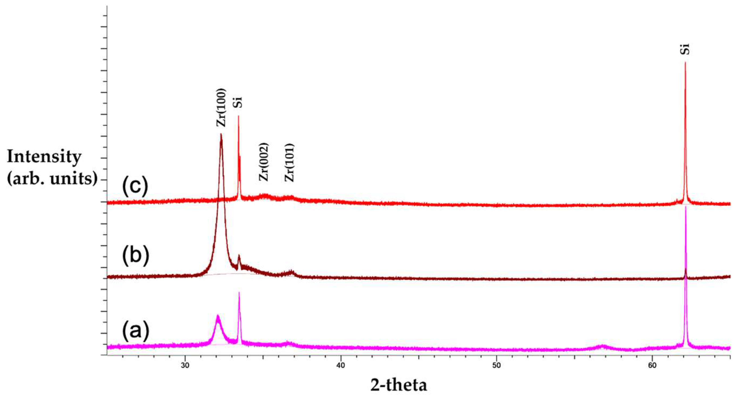
3.1.2. Effect of Temperature (XRD)

When the laser incident energy is constant, the atomic kinetic energy during deposition is mainly influenced by the substrate temperature. At high temperatures, the atoms on the film surface move rapidly to the lowest energy sites. This results in the formation of a low-energy structure. Consequently, Zr thin films deposited at high substrate temperatures have a larger thickness and a greater number of grains with c-axis orientation, leading to a smoother XRD curve and a stronger intensity of the Zr peak. The crystallinity of the sample improves with temperature, accordingly. However, an excessive substrate temperature can cause adatoms to decompose and re-evaporate from the surface, rendering the Zr film thermodynamically unstable and degrading the film’s thickness and crystalline quality.
We also performed depositions to investigate the effect of substrate temperature on Zr film morphology. The XRD data shown in Figure 3 were obtained for thin films synthesized using a 532 nm wavelength at three different substrate temperatures: 25 °C, 300 °C and 500 °C. The fluence was held constant at 0.52 J/cm2 for the proper analysis of the substrate temperatures. The peak corresponding to Zr (100) at 25 °C was much lower in intensity compared to the peak at 300 °C; however, this peak was not visible at 500 °C. The change in peak intensity was different for the Zr (002) peak. At 25 °C, a peak with very low intensity was obtained. This peak significantly increased in intensity at 300 °C but returned to its initial intensity at 500 °C.
It should be noted that high substrate temperatures provide more energy for the mobility of the adatoms on the surface and increase the hopping rate. However, further increases in the substrate temperature may induce thermal stress due to thermal expansion coefficient mismatch between the substrate and the coating. The silicon thermal expansion coefficient is 2.5 × 10⁻⁶ K and the average coefficients of thermal expansion of hexagonal zirconium between 298 °K and 1143 °K are 5.5 × 10⁻⁶ deg−1 along the a axis, 10.8 × 10⁻⁶ deg−1 along the c axis, and 7.2 × 10⁻⁶ deg−1 for a randomly oriented polycrystalline sample. The average value of the linear coefficient of expansion of cubic zirconium between 1143 °K and 1600 °K is 9.7 × 10⁻⁶ deg−1 [32]. In addition, crystallization cannot occur below a certain critical thickness, which is set by the energy difference between the coating and the substrate. An additional increase in temperature after 300 °C increased the thermal stress with rapidly decreasing film thickness. This could further explain the difference in crystallinity between 300 and 500 °C.
The Zr (101) peak was only observed for the 25 °C substrate temperature; it was invisible for 300 °C and 500 °C. Furthermore, the Zr (102) peak was not observed for 25 °C or 300 °C, while a broad peak with a low intensity was observed at 500 °C. A similar phenomenon was observed for the PLD of iridium on Si(100) using the third harmonic of Nd:YAG laser in the substrate temperature range of 200–400 °C [33]. It was observed that while there were other peaks of iridium at 200–400 °C, there was a dominant Ir (111) peak at a temperature range of 200–300 °C, as a dominant Zr (100) peak was observed in our case at 300 °C.
Moreover, XRD data of bismuth thin films deposited with a 248 nm excimer laser in a substrate temperature range of −40–200 °C showed a similar pattern to our XRD data of a Zr thin film deposited in a temperature range of RT—500 °C [34]. From −40–30 °C, the intensity of peaks was low and only visible with GIXRD, confirming the polycrystalline nature of the thin film. From −30 °C to 50 °C, one dominant peak of Ir (111) existed, and finally from 50 °C to 200 °C multiple peaks were observed without any preferred orientation. This result is similar in the sense that we observed some peaks at RT, but their intensity was low. Similarly, at 300 °C, a single dominant peak was observed, and finally at 500 °C there were multiple peaks without any observable orientation.
We previously found that the substrate temperature is a critical factor in determining the phase of the NbNx films. For a substrate temperature up to 450 °C, the film showed poor crystalline quality. With a temperature increase, the film became more textured. For a substrate temperature of 650−850 °C, a mix of cubic NbN and hexagonal phases were formed, and the surface roughness of the NbNx films increased as the temperature was raised from 450 °C to 850 °C [15].
Figure 4 illustrates the XRD data for Zr thin films obtained at three different substrate temperatures, 25 °C, 300 °C, and 500 °C, with 0.52 J/cm2 fluence using a 1064 nm wavelength. The peak corresponding to Zr (100) showed a similar pattern compared to the Zr (100) peak of 532 nm, i.e., the peak intensity increased from 25 °C to 300 °C and the peak disappeared at 500 °C. The Zr (002) and Zr (101) peaks were not observable for 25 °C and 300 °C; however, they were barely observable at 500 °C. The peak corresponding to Zr (102) were not observed for all three temperatures. In both cases, the dominant peak was obtained at a 300 °C substrate temperature, with the peak corresponding to Zr (100) Miller indices.
When the crystallinity of Zr thin films for substrate temperatures 25 °C and 300 °C was compared according to wavelength, the films produced using 532 nm were more crystalline as the ratio between the height of the Zr (100) peak and its width was larger.

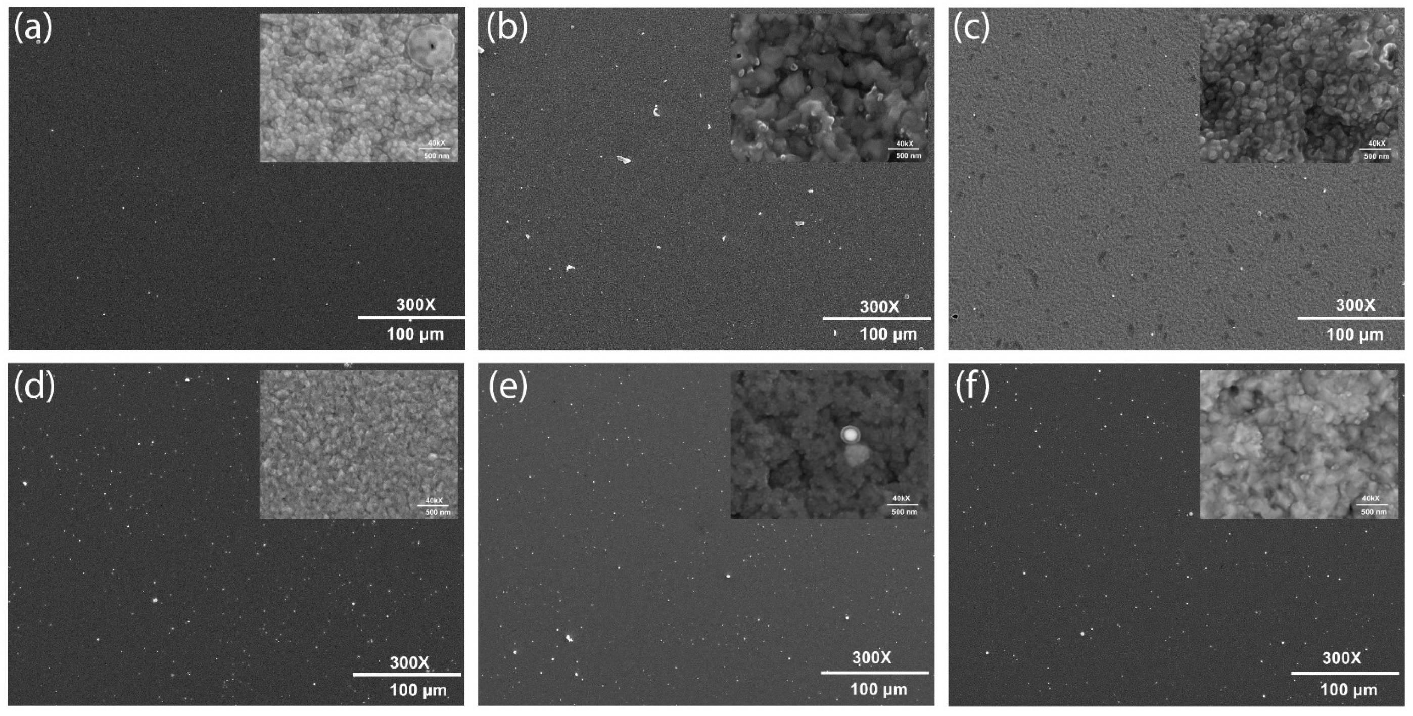
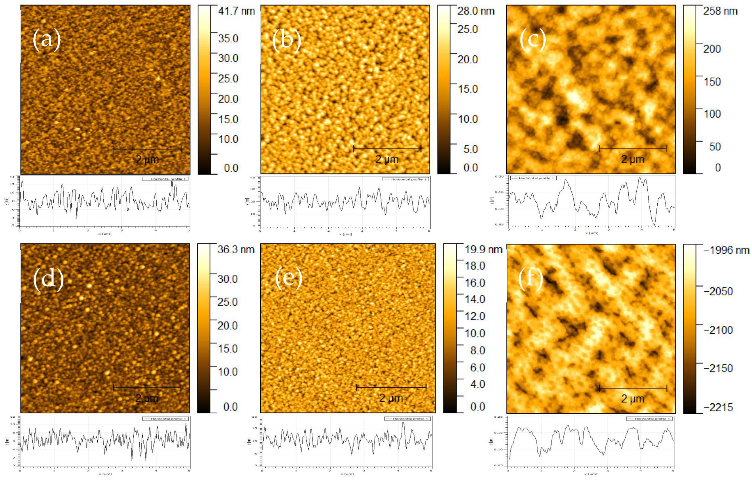
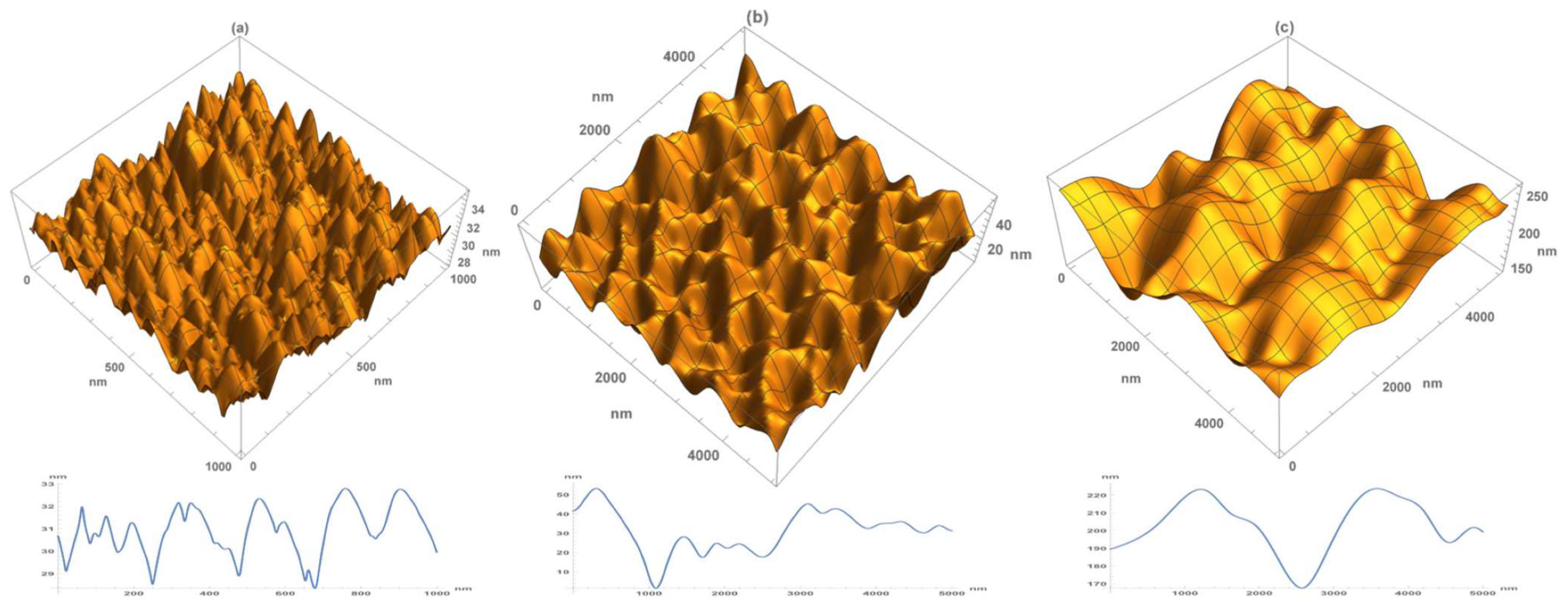
3.1.3. Morphology (Effect of Fluence)

Scanning electron microscopy (SEM) images shown in Figure 5 correspond to thin films deposited at a substrate temperature of 500 °C using both a 1064 nm and a 532 nm Nd: YAG laser at three different fluences. Magnified images seen as inset images in Figure 5 show a more coarse-grained surface pattern at higher fluence for both wavelengths.
Figure 6 shows the corresponding atomic force microscopy (AFM) images of these Zr thin films. When the surfaces of the thin films are compared according to wavelength for the same conditions as the Zr thin films, clear morphological differences can be observed.
Irregular pits can be observed for the 500 °C substrate temperature. The depth of the pits became bigger with the fluence, leading to a surface roughness increase. There are some rectangular structures observable on the surface shown in Figure 6a, which corresponds to the 0.26 J/cm2 fluence and substrate temperature of 500 °C Zr thin film for the 1064 nm wavelength. These rectangular structures changed to more irregular pits as the fluence changed to 0.52 J/cm2 and 1.04 J/cm2. The roughness of the film increased from ~22 nm to 27 nm when the fluence changed to 0.52 J/cm2 and 1.04 J/cm2.
Similar results were observed in the PLD of platinum deposited on MgO using the ArF excimer laser (193 nm) at 1 × 10⁻⁵ Torr (oxygen) pressure at a 850 °C substrate temperature for fluences lower than 1.92 J/cm2. It was determined that the roughness increased with increasing fluence [35]. However, the surface roughness dropped abruptly above the 1.92 J/cm2 fluence. This difference could be due to the use of partial oxygen pressure. Furthermore, the MgO thin film deposited at 100 °C using a 532 nm Nd:YAG laser showed an increase in the surface roughness as the fluence increased [36]. Our previous result also showed that the surface roughness of the NbNx film increased when the temperature was raised from 450 °C to 850 °C [15].
For Zr thin films deposited at the 1064 nm wavelength, structures that are more irregular were observed as compared to the 532 nm thin films, as seen in Figure 6d–f. However, the surface roughness was smaller for the 1064 nm wavelength, as compared to the 532 nm wavelength obtained from the AFM images.
For instance, the surface roughness of the coating obtained at 500 °C with 532 nm was around 25 nm, but it decreased to 22 nm with 1064 nm.
Moreover, thin films deposited at the 1.04 J/cm2 fluence were coarser as compared to the lower fluences for both 1064 nm and 532 nm wavelengths. Our results indicate that surface roughness is strongly affected by wavelength, laser fluence, and temperature.

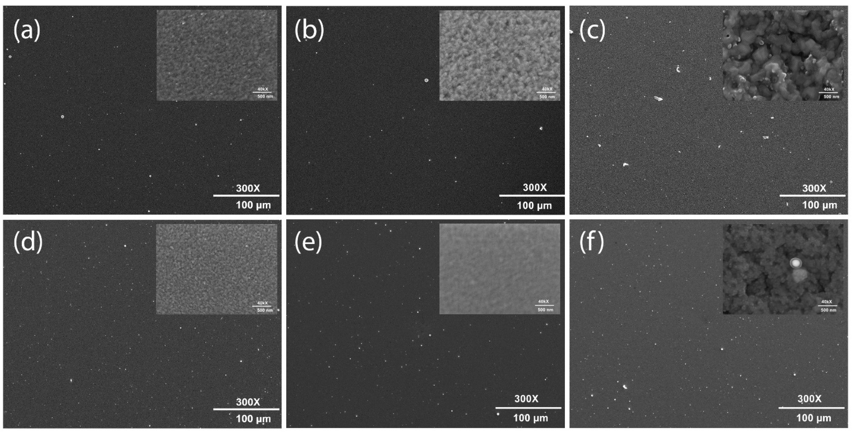
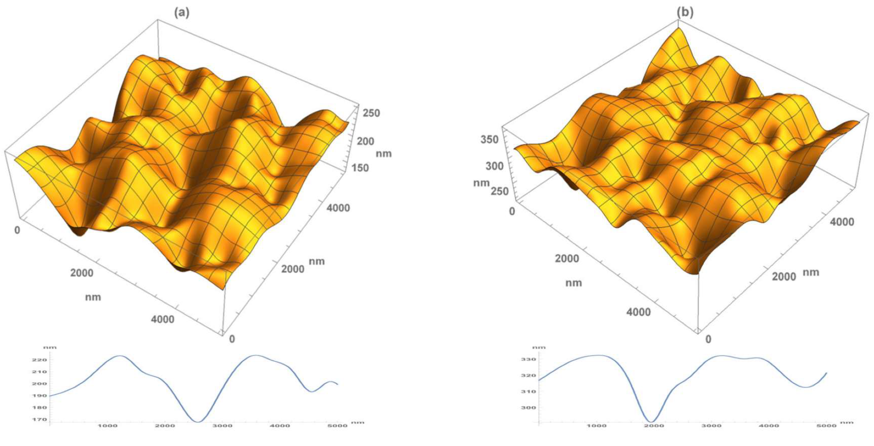
3.1.4. Morphology (Effect of Temperature)

Temperature is known to affect many properties of the film during and after deposition. At higher temperatures, adatoms on the substrate’s surface gain thermal energy and the surface diffusion is enhanced, thus promoting crystal growth. The transition from a textured microstructure to a densely packed crystal structure occurs over a range of temperatures.
To study the effect, Zr thin films were deposited at three different substrate temperatures: RT, 300 °C, and 500 °C at 532 nm and 1064 nm. SEM images in Figure 7 show smaller grains for RT, which increase as the substrate temperature is raised to 300 °C. A further increase in the substrate temperature to 500 °C results in the formation of deeper pits and rectangular structures, thus resulting in an increase in the surface roughness for both wavelengths.
Figure 8 shows the AFM images obtained for the Zr thin films at the three different substrate temperatures, with a fluence of 0.52 J/cm2. The structural characteristics and surface patterns observed in the AFM images are congruent with those observed in the SEM images of Figure 7.
For the 532 nm wavelength at 25 °C, the surface roughness was the smallest. There was a slight increase when the substrate temperature was increased to 300 °C, but there was a more distinct increase in surface roughness from 300 °C to 500 °C due to the formation of pits. A similar pattern was observed for the 1064 nm thin films; however, films obtained at 532 nm were rougher and the surface roughness increased with the temperature.
A similar pattern was observed for the PLD of iridium on the Si(100) substrate using the third harmonic of the Nd:YAG laser [33]. Moreover, the effect of the substrate temperature on the PLD of carbon using both 532 nm and 1064 nm was studied, and it was found that thin films produced using a 1064 nm wavelength were smoother in comparison to the ones deposited at 532 nm. Additionally, the temperature dependence of the surface roughness was stronger for 532 nm as compared to 1064 nm for the temperature range of 200 °C to 400 °C [37]. Our result was similar for 25 °C and 300 °C.
An increase in surface roughness as a function of substrate temperature was observed in diamond-like carbon (DLC) thin films using a 248 nm excimer laser in the temperature range 25–300 °C [38]. Similar results were obtained for bismuth thin films deposited using a 248 nm excimer laser in the temperature range of −40 °C to 200 °C [34].
Zeng et al. [39] and Liu et al. [40] conducted studies on the deposition of ZnO films on substrates at different temperatures. Zeng et al. found that the deposition rate decreased but the crystalline quality improved at temperatures above 400 °C, as compared to lower temperatures. Liu et al. obtained similar results for deposition on glass and silicon substrates [41,42]. However, a higher quality crystalline nature of ZnO thin films grown on a Si(111) substrate at 600 °C was observed [43]. The surface roughness was found to be closely correlated with the substrate temperature due to variations in grain size. Typically, grain size increases with an increase in substrate temperature, therefore increasing the surface roughness [42,43,44]. At significantly high temperatures, the re-evaporation of atoms from the surface occurs.
To provide a theoretical insight into the growth mechanisms of a Zr film, we conducted computations based on a slightly modified but still well-known continuum model of thin film growth [44,45]. In our model the film grows due to Zr atoms adsorbing from a vapor (formed by the ablated species) on the film surface; this adsorption and the surface diffusion of adatoms also contribute to changes of the film morphology during growth. This may lead to a formation of islands, followed by the island coarsening. The evolution equation for the film height h in our model is:
h t = F 1 + | h | 2 + D s 2 μ λ [ ( 1 s 2 | h | 2 ) h ] .
The first term in the above equation describes film growth by the atomic flux F from a vapor, the second term describes the surface diffusion of adatoms, and the third term describes the Ehrlich-Schwoebel effect that is responsible for islands formation. λ is the Ehrlich-Schwoebel parameter, s the equilibrium mound slope, s 2 the surface Laplacian, μ = γ κ + n 3 γ h the surface chemical potential, and D = Ω 2 D s ν k T the diffusion parameter. Here, κ is the surface mean curvature, n 3 the third component of the surface normal vector, Ω the atomic volume, D s = D 0 exp [ E a / k T ] the surface diffusion coefficient, ν the surface density of adatoms, kT the Boltzmann’s factor, and γ ( h ) the surface energy [45]. The last term in the chemical potential describes the effect of the substrate wetting by the film. The film thickness and morphology depend in a very complex way on F, D, λ , s, and the parameters of the surface energy function γ ( h ) . After fixing all material constants and temperature, we tuned F, λ , and s so that the computed maximum film thickness roughly matched the one in the experiment after one hour of deposition (since the surface diffusion coefficient of Zr was not available, we used the pre-factor and the activation energy that corresponded to Si/Si(100) [46]).
Computation results are shown in Figure 9 and Figure 10. In Figure 9, similar to Figure 8, as the temperature increases, the surface morphology becomes coarser. This is attributed to faster surface mass transport. At room temperature, laterally very small islands of a maximum height of 7 nm were observed. At 300 °C and 500 °C, the islands were much wider and higher after one hour. Their total height was 40 nm at 300 °C and 100 nm at 500 °C. Overall, at higher temperatures the film morphology resembled a large hill-and-valley pattern, seen in Figure 8c,f. In Figure 10, it can be seen that at a larger atomic flux F, the islands’ height increased significantly and again the morphology was coarser, i.e., the lateral scale of the pattern was larger. This matched the experiment results shown in Figure 6.

4. Summary

We deposited zirconium thin films on silicon using the pulsed laser deposition technique at different wavelengths, temperatures, and fluences. Our results show that temperature, wavelength, and laser fluence play critical roles in determining the structural and phase properties of zirconium. Our computations based on the continuum model of film growth agree with experimental observation. In addition, we showed that crystalline zirconium thin films can be obtained with 1064 and 532 nm laser wavelengths. In future work, we plan to deposit aluminum and zirconium multilayer coatings using PLD for the detection of solar flares in extreme UV regions.

Author Contributions

Methodology, Z.K., Y.A., I.M., M.K. and A.O.E.; validation, S.K.; investigation, I.M. and J.T.; data curation, A.O.E.; writing—original draft preparation, M.K. and A.O.E.; writing—review and editing, D.G. and A.O.E. All authors have read and agreed to the published version of the manuscript.

Funding

This project is funded by NASA Grant 635114, KY NSF EPSCoR 3048115832-23-186 and WKU RCAP 21-089.

Institutional Review Board Statement

Not applicable.

Informed Consent Statement

Not applicable.

Data Availability Statement

Not applicable.

Conflicts of Interest

The authors declare no conflict of interest.

References

  1. Nielsen, H.R.; Schlewitz, H.J.; Nielsen, H. Zirconium and Zirconium Compounds. In Kirk-Othmer Encyclopedia of Chemical Technology; Wiley & Sons: Hoboken, NJ, USA; pp. 1–46. Available online: https://www.samaterials.com/content/the-application-of-zirconium-products.html (accessed on 15 August 2023).
  2. Romanov, R.I.; Zuev, V.V.; Fominskii, V.Y.; Demin, M.V.; Grigoriev, V.V. Electrical properties of thin-film structures formed by pulsed laser deposition of Au, Ag, Cu, Pd, Pt, W, Zr metals on n-6 H-SiC crystal. Semiconductors 2010, 44, 1192–1198. [Google Scholar] [CrossRef]
  3. Fankhauser, J.; Sato, M.; Yu, D.; Ebnonnasir, A.; Kobashi, M.; Goorsky, M.S.; Kodambaka, S. Growth and characterization of epitaxial Zr(0001) thin films on Al2O3(0001). J. Vac. Sci. Technol. A 2016, 34, 050606. [Google Scholar] [CrossRef]
  4. Ogugua, S.N.; Ntwaeaborwa, O.M.; Swart, H.C. Latest Development on Pulsed Laser Deposited Thin Films for Advanced Luminescence Applications. Coatings 2020, 10, 1078. [Google Scholar] [CrossRef]
  5. Duta, L.; Mihailescu, I.N. Advances and Challenges in Pulsed Laser Deposition for Complex Material Applications. Coatings 2023, 13, 393. [Google Scholar] [CrossRef]
  6. Irimiciuc, S.A.; Chertopalov, S.; Lancok, J.; Craciun, V. Langmuir Probe Technique for Plasma Characterization during Pulsed Laser Deposition Process. Coatings 2021, 11, 762. [Google Scholar] [CrossRef]
  7. Duta, L.; Popescu, A.C. Current Research in Pulsed Laser Deposition. Coatings 2021, 11, 274. [Google Scholar] [CrossRef]
  8. Abdisatarov, B.; Ilhom, S.; Kholikov, K.; Loomis, D.; Dobrokhotov, V.; Khenner, M.; Er, A.O. Morphology and structure of Pb thin films grown on Si(111) by pulsed laser deposition. Appl. Phys. A 2020, 126, 1–7. [Google Scholar] [CrossRef]
  9. Axente, E.; Socol, G. Special Issue “Pulsed Laser Deposition of Thin Films: Recent Advances and Challenge”. Coatings 2022, 12, 368. [Google Scholar] [CrossRef]
  10. Jessadaluk, S.; Khemasiri, N.; Kayunkid, N.; Rangkasikorn, A.; Wirunchit, S.; Tammarugwattana, N.; Mano, K.; Chananonnawathorn, C.; Horprathum, M.; Klamchuen, A.; et al. Influence of Antimony Species on Electrical Properties of Sb-Doped Zinc Oxide Thin Films Prepared by Pulsed Laser Deposition. Nanomaterials 2023, 13, 1799. [Google Scholar] [CrossRef]
  11. Li, B.; Yang, H.-L.; Holmes, R.; Cui, L.-J.; Kano, S.; Abe, H. Thermal stability of the Cr-coated zirconium alloy microstructure prepared by pulsed laser deposition. Tungsten 2023, 8, 1–9. [Google Scholar] [CrossRef]
  12. Liu, W.; Wen, C.; Liu, Q.; Mao, L.; Zhou, X.; Long, X.; Peng, S. The effects of deuteration on the nanostructured zirconium films deposited by pulsed laser deposition for nuclear fusion applications. J. Nucl. Mater. 2015, 461, 325–328. [Google Scholar] [CrossRef]
  13. Benouareth, K.; Tristant, P.; Jaoul, C.; Le Niniven, C.; Nouveau, C.; Dublanche-Tixier, C.; Bouabellou, A. Study of the interaction between a zirconium thin film and an EN C100 steel substrate: Temperature effect. Vacuum 2016, 125, 234–239. [Google Scholar] [CrossRef]
  14. Farha, A.H.; Er, A.O.; Ufuktepe, Y.; Myneni, G.; Elsayed-Ali, H.E. Effects of substrate temperature on properties of NbNx films grown on Nb by pulsed laser deposition. Appl. Surf. Sci. 2011, 258, 1613–1618. [Google Scholar] [CrossRef]
  15. Rodríguez-Hernández, E.P.; Quiñones-Galván, J.; Meléndez-Lira, M.; Santos-Cruz, J.; Contreras-Puente, G.; de Moure-Flores, F. Effect of laser fluence on structural and optical properties of CuxS films grown by pulsed laser deposition at different wavelengths. Mater. Res. Express 2019, 7, 015908. [Google Scholar] [CrossRef]
  16. Ojeda-G-P, A.; Döbeli, M.; Lippert, T. Influence of Plume Properties on Thin Film Composition in Pulsed Laser Deposition. Adv. Mater. Interfaces 2018, 5, 1701062. [Google Scholar] [CrossRef]
  17. Khuzhakulov, Z.; Kylychbekov, S.; Allamyradov, Y.; Majidov, I.; Ben Yosef, J.; Er, A.Y.; Kitchens, C.; Banga, S.; Badarudeen, S.; Er, A.O. Formation of picosecond laser-induced periodic surface structures on steel for knee arthroplasty prosthetics. Front. Met. Alloy. 2023, 1, 1090104. [Google Scholar] [CrossRef]
  18. Huang, J.; Xu, K.; Xu, S.; Li, X.; Wei, Q.H. Self-Aligned Laser-Induced Periodic Surface Structures for Large-Area Controllable Nanopatterning. Laser Photonics Rev. 2022, 16, 2200093. [Google Scholar] [CrossRef]
  19. Zhang, D.; Liu, R.; Li, Z. Irregular LIPSS produced on metals by single linearly polarized femtosecond laser. Int. J. Extreme Manuf. 2022, 4, 015102. [Google Scholar] [CrossRef]
  20. Rivera, L.; Munoz-Martin, D.; Chávez-Chávez, A.; Morales, M.; Gómez-Rosas, G.; Molpeceres, C. Subwavelength LIPSS formation on SS304 by picosecond laser irradiation under water confinement. Mater. Sci. Eng. B 2021, 273, 115393. [Google Scholar] [CrossRef]
  21. Wicklein, S.; Sambri, A.; Amoruso, S.; Wang, X.; Bruzzese, R.; Koehl, A.; Dittmann, R. Pulsed laser ablation of complex oxides: The role of congruent ablation and preferential scattering for the film stoichiometry. Appl. Phys. Lett. 2012, 101, 13. [Google Scholar] [CrossRef]
  22. Ohnishi, T.; Hang, B.; Xu, X.; Osada, M.; Takada, K. Quality control of epitaxial LiCoO2 thin films grown by pulsed laser deposition. J. Mater. Res. 2010, 25, 1886–1889. [Google Scholar] [CrossRef]
  23. Kan, D.; Shimakawa, Y. Controlled cation stoichiometry in pulsed laser deposition-grown BaTiO3 epitaxial thin films with laser fluence. Appl. Phys. Lett. 2011, 99, 081907. [Google Scholar] [CrossRef]
  24. Schou, J. Physical aspects of the pulsed laser deposition technique: The stoichiometric transfer of material from target to film. Appl. Surf. Sci. 2009, 255, 5191–5198. [Google Scholar] [CrossRef]
  25. Sigmund, P. Sputtering by ion bombardment theoretical concepts. In Sputtering by Particle Bombardment I: Physical Sputtering of Single-Element Solids; Behrisch, R., Ed.; Springer: Berlin/Heidelberg, Germany, 1981; pp. 9–71. [Google Scholar]
  26. Bäuerle, D. Laser Processing and Chemistry; Springer Science & Business Media: Berlin/Heidelberg, Germany, 2013. [Google Scholar]
  27. Chen, L.C.; Chrisey, D.B.; Hubler, G.K. Hubler, Pulsed Laser Deposition of Thin Films; Wiley: New York, NY, USA, 1994. [Google Scholar]
  28. Kautek, W.; Roas, B.; Schultz, L. Formation of Y-Ba-Cu-oxide thin films by pulsed laser deposition: A comparative study in the UV, visible and IR range. Thin Solid Films 1990, 191, 317–334. [Google Scholar] [CrossRef]
  29. Liu, H.; Mao, X.; Yoo, J.; Russo, R. Early phase laser induced plasma diagnostics and mass removal during single-pulse laser ablation of silicon. Spectrochim. Acta Part B At. Spectrosc. 1999, 54, 1607–1624. [Google Scholar] [CrossRef]
  30. Liu, W.; Liang, J.; Zhou, X.; Long, X. Formation of zirconium silicide between silicon substrate and zirconium films. Mater. Lett. 2014, 122, 220–222. [Google Scholar] [CrossRef]
  31. Skinner, G.B.; Johnston, H.L. Thermal Expansion of Zirconium between 298 and 1600 K. J. Chem. Phys. 1953, 21, 1383–1384. [Google Scholar] [CrossRef]
  32. Gong, Y.; Wang, C.; Shen, Q.; Zhang, L. Low-temperature deposition of iridium thin films by pulsed laser deposition. Vacuum 2008, 82, 594–598. [Google Scholar] [CrossRef]
  33. Wu, K.-S.; Chern, M.-Y. Temperature-dependent growth of pulsed-laser-deposited bismuth thin films on glass substrates. Thin Solid Films 2008, 516, 3808–3812. [Google Scholar] [CrossRef]
  34. Takai, Y.; Sato, M. Epitaxial growth of platinum thin films on (100) MgO by pulsed laser deposition. Supercond. Sci. Technol. 1999, 12, 486–490. [Google Scholar] [CrossRef]
  35. Ismail, R.A.; Mousa, A.M.; Shaker, S.S. Preparation of visible-enhanced PbI2/MgO/ Si heterojunction photodetector. Optik 2019, 202, 163585. [Google Scholar] [CrossRef]
  36. Yoshitake, T.; Nishiyama, T.; Aoki, H.; Suizu, K.; Takahashi, K.; Nagayama, K. The effects of substrate temperature and laser wavelength on the formation of carbon thin films by pulsed laser deposition. Diam. Relat. Mater. 1999, 8, 463–467. [Google Scholar] [CrossRef]
  37. Modabberasl, A.; Sharifi, M.; Shahbazi, F.; Kameli, P. Multifractal analysis of DLC thin films deposited by pulsed laser deposition. Appl. Surf. Sci. 2019, 479, 639–645. [Google Scholar] [CrossRef]
  38. Zeng, J.N.; Low, J.K.; Ren, Z.M.; Liew, T.; Lu, Y.F. Effect of deposition conditions on optical and electrical properties of ZnO films prepared by pulsed laser deposition. Appl. Surf. Sci. 2002, 197–198, 362–367. [Google Scholar] [CrossRef]
  39. Liu, M.; Wei, X.; Zhang, Z.; Sun, G.; Chen, C.; Xue, C.; Zhuang, H.; Man, B. Effect of temperature on pulsed laser deposition of ZnO films. Appl. Surf. Sci. 2005, 252, 4321–4326. [Google Scholar] [CrossRef]
  40. He, J.; Zhuang, H.; Xue, C.; Wang, S.; Hu, L.; Xue, S. Effect of substrate temperature on microstructural and optical properties of ZnO films grown by pulsed laser deposition. Rare Met. 2006, 25, 161–165. [Google Scholar] [CrossRef]
  41. Kang, S.J.; Joung, Y.H.; Shin, H.H.; Yoon, Y.S. Effect of substrate temperature on structural, optical and electrical properties of ZnO thin films deposited by pulsed laser deposition. J. Mater. Sci. Mater. Electron. 2007, 19, 1073–1078. [Google Scholar] [CrossRef]
  42. Son, C.S.; Kim, S.M.; Kim, Y.H.; Kim, S.I.; Kim, Y.T.; Yoon, K.H.; Choi, I.-H.; Lopez, H.C. Deposition-temperature dependence of ZnO/Si grown by pulsed laser deposition. J. Korean Phys. Soc. 2004, 45, 685–688. [Google Scholar]
  43. Ryu, Y.R.; Zhu, S.; Budai, J.D.; Chandrasekhar, H.R.; Miceli, P.F.; White, H.W. Optical and structural properties of ZnO films deposited on GaAs by pulsed laser deposition. J. Appl. Phys. 2000, 88, 201–204. [Google Scholar] [CrossRef]
  44. Ortiz, M.; Repetto, E.; Si, H. A continuum model of kinetic roughening and coarsening in thin films. J. Mech. Phys. Solids 1999, 47, 697–730. [Google Scholar] [CrossRef]
  45. Korzec, M.D.; Evans, P.L. From bell shapes to pyramids: A reduced continuum model for self-assembled quantum dot growth. Phys. D Nonlinear Phenom. 2010, 239, 465–474. [Google Scholar] [CrossRef]
  46. Liu, F.; Lagally, M. Epitaxial growth of Si on Si(001). In The Chemical Physics of Solid Surfaces; Elsevier: Amsterdam, The Netherlands, 1997; pp. 258–296. [Google Scholar]
Figure 1. XRD data for Zr thin films deposited with a wavelength of 532 nm, fluences of (a) 0.26 J/cm2, (b) 0.52 J/cm2, and (c) 1.04 J/cm2, and substrate temperature of 500 °C.
Coatings 13 01748 g001
Figure 2. XRD data for Zr thin films deposited with a wavelength of 1064 nm, fluences of (a) 0.26 J/cm2, (b) 0.52 J/cm2, and (c) 1.04 J/cm2, and substrate temperature of 500 °C.
Coatings 13 01748 g002
Figure 3. XRD data for Zr thin films deposited with a wavelength of 532 nm, fluence of 0.52 J/cm2, and substrate temperatures of (a) 25 °C, (b) 300 °C, and (c) 500 °C.
Coatings 13 01748 g003
Figure 4. XRD data for Zr thin films deposited with wavelength of 1064 nm, fluence 0.52 J/cm2, and substrate temperatures of (a) 25 °C, (b) 300 °C, (c) 500 °C.
Coatings 13 01748 g004
Figure 5. SEM data for Zr thin films deposited with a wavelength of 532 nm, fluences (a) 0.26 J/cm2, (b) 0.52 J/cm2, and (c) 1.04 J/cm2, and substrate temperature of 500 °C, and with a wavelength of 1064 nm and fluences of (d) 0.26 J/cm2, (e) 0.52 J/cm2, and (f) 1.04 J/cm2.
Coatings 13 01748 g005
Figure 6. AFM data for Zr thin films deposited with a wavelength of 532 nm, fluences (a) 0.26 J/cm2, (b) 0.52 J/cm2, and (c) 1.04 J/cm2, and substrate temperature of 500 °C, and with a wavelength of 1064 nm, fluences of (d) 0.26 J/cm2, (e) 0.52 J/cm2, and (f) 1.04 J/cm2, and substrate temperature of 500 °C.
Coatings 13 01748 g006
Figure 7. SEM data for Zr thin films deposited with fluence 0.52 J/cm2 and a wavelength of 532 nm and substrate temperatures of (a) 25 °C, (b) 300 °C, and (c) 500 °C, and with a wavelength of 1064 nm and substrate temperatures of (d) 25 °C, (e) 300 C, and (f) 500 °C.
Coatings 13 01748 g007
Figure 8. AFM data for Zr thin films deposited with a wavelength of 532 nm, fluence 0.52 J/cm2, and substrate temperatures of (a) 25 °C, (b) 300 °C, and (c) 500 °C, and a wavelength of 1064 nm, fluence 0.52 J/cm2, and substrate temperatures of (d) 25 °C, (e) 300 °C, and (f) 500 °C.
Coatings 13 01748 g008
Figure 9. Computational results. Surface morphology is shown after 1 hr of film growth at substrate temperatures of (a) 25 °C, (b) 300 °C, and (c) 500 °C. Note that the scale along the x and y axes in the panel (a) is five times smaller than in the panels (b,c).
Coatings 13 01748 g009
Figure 10. Computational results. Surface morphology is shown after 1 hr of film growth at a substrate temperature of 500 °C. The atomic flux F in the panel (b) is 25% higher than in the panel (a).
Coatings 13 01748 g010
Disclaimer/Publisher’s Note: The statements, opinions and data contained in all publications are solely those of the individual author(s) and contributor(s) and not of MDPI and/or the editor(s). MDPI and/or the editor(s) disclaim responsibility for any injury to people or property resulting from any ideas, methods, instructions or products referred to in the content.

