Article

Suppression of Secondary Electron Emissions on the Graphene-Coated Polyimide Materials Prepared by Chemical Vapor Deposition

1
School of Power and Mechanical Engineering, Wuhan University, Wuhan 430072, China
2
Beijing Institute of Spacecraft Environment Engineering, Beijing 100086, China
3
Wuhan Second Ship Design and Research Institute, Wuhan 430205, China
*
Authors to whom correspondence should be addressed.
Coatings 2023, 13(10), 1805; https://doi.org/10.3390/coatings13101805
Submission received: 22 September 2023 / Revised: 8 October 2023 / Accepted: 17 October 2023 / Published: 20 October 2023

Abstract

:
Polyimide thin-film materials are widely used in aerospace and particle gas pedals, etc., but the phenomenon of secondary electron emission occurred under vacuum conditions. The graphene-coated polyimide materials were prepared for this phenomenon to suppress secondary electron emissions. The graphene coating was prepared on the polyimide surface through chemical vapor deposition (CVD). Scanning electron microscope images (SEM), X-ray photoelectron spectrometer images (XPS), Raman spectroscopy, atomic force microscopy (AFM), and other analytical methods were used to characterize the properties of the prepared materials. The C1s XPS fine spectra and Raman curve analyses showed that the material has an abundant sp2 hybridized structure, and the sp2 structure can reduce secondary electron emissions. The C, O, and N contents in the tested samples were 65.85, 20.47, and 13.68 at.%, respectively. It was examined that the graphene coating had an inhibitory effect on the secondary electron emissions of polyimide materials, and the secondary electron emission yield (SEY) was significantly reduced. The results of secondary electron tests showed that the maximum SEY (δmax) of the polyimide material decreased from 1.72 to 1.52 after the preparation of the graphene coating. The mechanism of using a graphene coating to reduce the SEY of polyimide was analyzed from experimental and theoretical perspectives. The results of this study can provide research ideas for polyimide thin film materials in aerospace, particle gas pedals, and other applications.

1. Introduction

With the continuing development of science and technology, the demand for high-performance polymers in the field of coating has increased [1]. Polyimide as a polymeric high-performance polymer material is widely used in aerospace and particle gas pedals. However, polyimide is subject to surface charging and discharging phenomena in the environment of space (vacuum), and even weak surface discharge phenomena can cause catastrophic failures and serious economic losses to spacecraft and other vacuum devices. The secondary electron emission yield (SEY) is defined as the ratio between the number of electrons exiting the material and the number of incident electrons on the surface of the material. The SEY is an important characteristic parameter that determines the spaceflight surface charging potential, and it plays a crucial role in the assessment and prediction of satellite surface charging [2]. Therefore, it is important to reduce and suppress the secondary electron emissions from vacuum surfaces of a polyimide.
When a primary electron beam is incident inside a material, it excites electrons, causing them to leap, and generates secondary electrons. The secondary electrons can move toward the material surface at a certain depth and escape into the vacuum, which is called secondary electron emission [3]. In this paper, the electrons escaping into the vacuum with a kinetic energy below 50 eV are called secondary electrons. Electrons escaping into the vacuum with a kinetic energy higher than 50 eV are called backscattered electrons. Secondary electron emission is widely seen in many instruments and scenarios, and the phenomenon of secondary electron emission can have many undesirable effects [4,5]. In space systems, secondary electrons are generated on the surface of components due to space particle beam currents, so that microwave components can produce microdischarge effects. The microdischarge effect is likely to detune resonant-type devices and cause the escape of internal gases from the material surface, producing more severe discharges. It also subjects the component surface to electron erosion, causing the degradation of component performance, etc. [6,7]. In particle gas pedals, the electron cloud effect generated by the secondary electron emission phenomenon on the surface of the vacuum chamber material can seriously affect the operation of the gas pedal, and the electron cloud can affect the stability of the gas pedal beam, increase the thermal load of the vacuum device, decrease the vacuum level, etc. [8,9]. Therefore, it has become a consensus among researchers in the field of electric vacuum to reduce the SEY of materials in order to prevent the undesirable effects of secondary electron emissions [10,11,12,13].
Since secondary electron emission properties are related to the nature and surface morphology of the material itself [14], researchers usually suppress secondary electron emissions by increasing the roughness of the material surface or by adding coatings with low SEY to the surface [15,16,17,18]. Graphene coatings have attracted the attention of the worldwide scientific community due to their fascinating properties and great potential for various applications [19,20,21,22], and are also highly inert in air [23,24]. It is considered as a potential low-secondary-electron-emission material due to the low SEY resulting from having a sp2 hybridized structure [25]. Many researchers have prepared graphene coatings on copper, stainless steel, aluminum, and other metal surfaces to reduce the SEY with some desirable results. Meng Cao et al. [26] prepared single-layer graphene coatings on copper surfaces using chemical vapor deposition (CVD), and the maximum SEY decreased from 2.1 to 1.5. Jie Wang et al. [27] deposited graphene coatings with different numbers of layers on copper surfaces, and the maximum SEY was 1.25 when the number of graphene layers was 6–8. Taaj Sian et al. [28] deposited graphene coatings on the surface of stainless a steel substrate using electrophoretic deposition (EPD), which decreased the maximum SEY of stainless steel from 2.4 to 1.4. R. Aguincha et al. [29] used EPD to deposit graphene on stainless steel and copper, and the maximum total electron yield decreased to 1.04. Jun Luo et al. [30] demonstrated that graphene meets the stringent requirements of weight, volume, and power consumption for communication and space detectors. The CVD method is one of the most commonly used methods in plating preparation studies, with simpler and better controllability, and has promising applications for the suppression of secondary electron emissions in material coating preparation. However, no researcher has studied the suppression of secondary electron emissions from graphene coatings on polyimide materials.
In this paper, to reduce the secondary electron emission yield of polyimide thin film materials, a graphene coating was used. The graphene coating was prepared on the surface of polyimide materials using the CVD method. SEM, XPS, Raman spectroscopy, AFM, and other analytical methods were used to characterize the properties of the material. The morphology, structural integrity, and changes of functional groups of the coating after preparation were analyzed. The secondary electron emission performance of the coating after preparation was tested. The mechanism of using a graphene coating to reduce the SEY of polyimide from experimental and theoretical perspectives was analyzed. The results of this study can provide research ideas for polyimide thin film materials in aerospace, particle gas pedals, and other applications.

2. Materials and Methods

2.1. Material Preparation

Polyimide material was selected from widely used aerospace polyimide film material (Shenzhen Ruihuatai Film Technology Co., Ltd., Shenzhen, China). The polyimide graphene coating preparation using the CVD method is shown in Figure 1. Graphene was obtained using the CVD method. The polyimide material was cut into a shape slightly larger than 1 cm × 1 cm, and then was put into the pre-prepared pretreatment solution (phosphoric acid and deionized water mixed solution, concentration of 6%). It was soaked for 10 min, and then washed in deionized water 2–3 times. The polyimide material was blow dried, the residual water on the surface was deionized with nitrogen, then the equipment was sealed. The baffle valve was slowly and evenly loosened until the air pressure in the furnace tube dropped to 0 Pa. The hydrogen gas was passed in 5000 Pa, and then was pumped off for the 2–3 times during the gas washing process. The flow rate of hydrogen on the airflow meter was set to 60 sccm. The experimental temperature was set to 950°, and the reading of the vacuum meter was always 0 Pa. The equipment was run, heated up, and timed for 90 min. The flow rate of hydrogen and methane on the airflow meter was set to 2 sccm:30 sccm after the heating up process. The air pressure inside the tube was adjusted to 1830 Pa–1860 Pa. Material was grown for an hour. The hydrogen gas, methane, as well as the heating procedure were shut down, and the equipment was cooled down to room temperature. The 1 cm × 1 cm graphene was taken on the homogenizer, and 1–2 drops of poly methyl methacrylate solution (PMMA) were used during spin coating. The graphene was put into the treatment solution (the ratio of ammonium persulfate: deionized water is 1:1) to etch after drying. It was rinsed on the whole of one side with deionized water after 3–5 min, and this process was repeated 3 times. The graphene was put into a clean etching solution (the ratio of concentrated hydrochloric acid: anhydrous copper sulfate: deionized water is 1:0.5:1) until etching was complete. After etching, the graphene was transferred to deionized water using a slide, and the graphene surface was cleaned by sucking deionized water with a dropper. This process was repeated 2–3 times. The air bubbles on the back of the graphene were removed with bubble removal film, and the target substrate was rinsed with alcohol and deionized water. The graphene was transferred to the middle of the substrate, then was put into the homogenizer to spin dry. Finally, it was put onto the drying table (50 °C–60 °C) to dry. The dried graphene was removed and cooled down to room temperature, put into a Petri dish with acetone, and soaked about 20 min. Then, it was immediately rinsed with a wash bottle containing acetone and alcohol, and was quickly dried on the baking table (100 °C–110 °C). The prepared samples were used to verify the number of graphene layers on the material surface by detecting the surface transmittance. In the end, the polyimide material with 1, 2, and 3 layers of graphene coating was obtained.

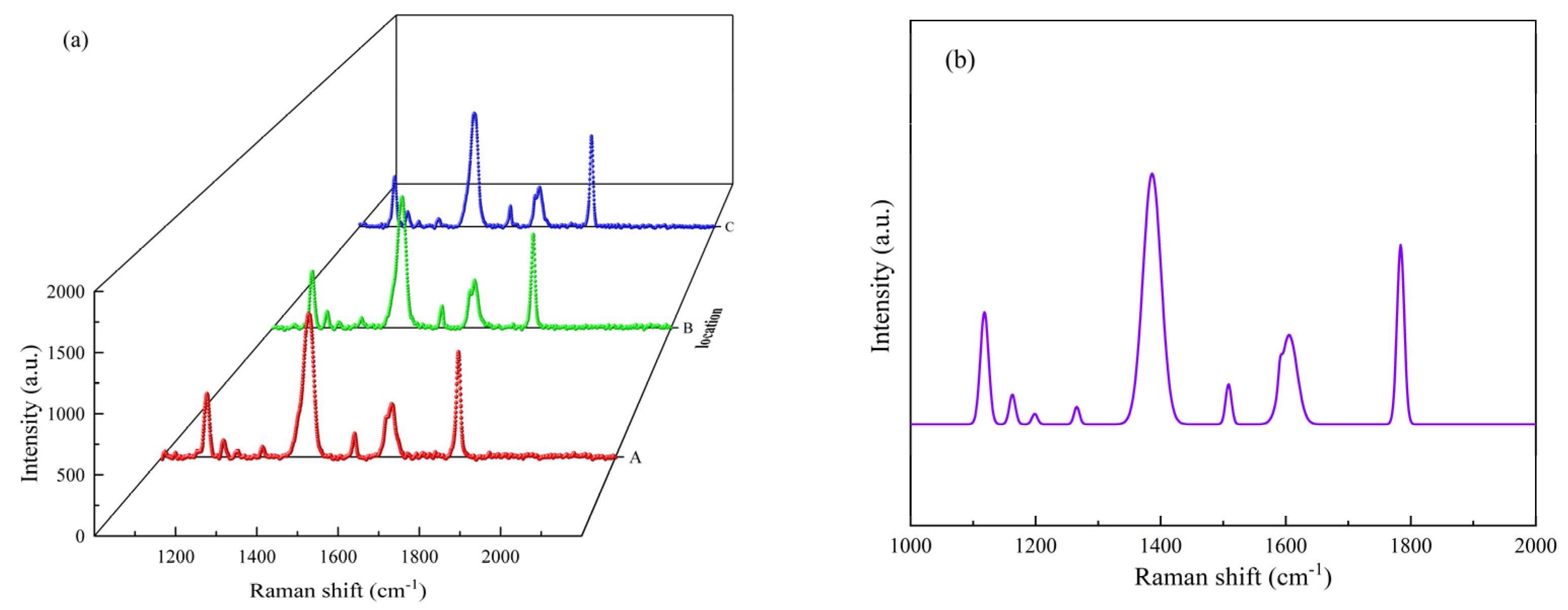
2.2. Material Characterization

The SEM images were acquired by a field emission scanning electron microscope (Carl Zeiss Germany, Zeiss SIGMA, Jena, Germany) to characterize the surface morphology of the graphene-coated polyimide materials using field emission scanning electron microscopy. X-ray photoelectron spectroscopy was acquired by an X-ray Photoelectron Spectrometer (Thermo Fisher Scientific, ESCALAB 250Xi, Waltham, MA, USA) with an optimal spatial resolution better than 20 μm, and an imaging XPS with a spatial resolution better than 3 μm was used to study the surface elemental composition of the modified samples. Raman spectroscopy was performed with a confocal Raman microscope (HORIBA Jobin Yvon, XploRA Plus, Longjumeau, France) to study the surface elemental composition of the modified samples, which have a laser wavelength of 785 nm, 10% attenuation, an integration time of 10 s/1 time, and a wave number in the test range: 60–3200 cm−1. Atomic force microscopy was performed using a Japanese atomic force microscope (Shimadzu, SPM-9700HT, Kyoto, Japan) to characterize the surface three-dimensional morphology and average roughness of the polyimide films.

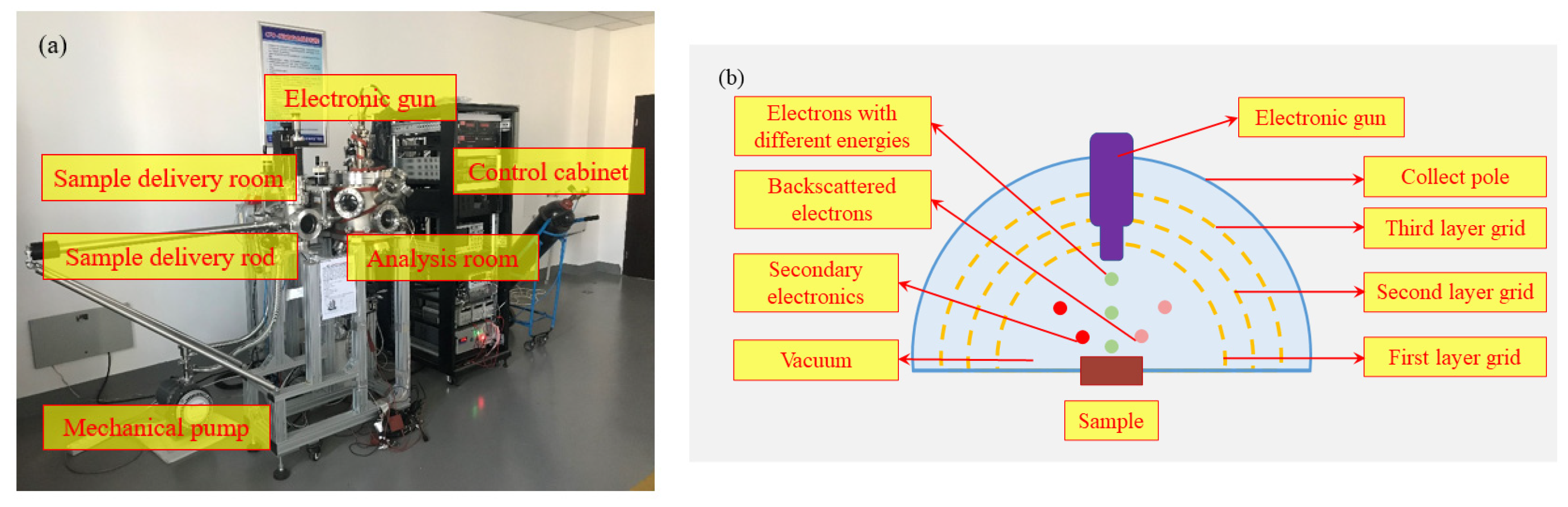
2.3. Secondary Electron Yield Measurement

The secondary electron measurement device was a homemade test device made by the Beijing Satellite Environment Institute, and the electron gun emits electrons in the energy range of 50–5000 eV. The secondary electronic measurement device mainly consists of an electronic gun, sample delivery room, sample delivery rod, mechanical pump, control cabinet, and analysis room. The secondary electronic measurement device and principle are shown in Figure 2. The test principle is that the electron gun emits electrons to the surface of the material, and the secondary electrons and backscattered electrons excited by the incident electrons will escape from the surface of the material and pass through the three-layer grid in turn; finally, the electrons will be collected by the collection pole. The secondary electrons and backscattered electrons of the different energies can be screened by applying different bias pressures to each layer of the grid. Eventually, the collection of secondary electrons and backscattered electrons were realized. When the sample, the three-layer grids, and the collecting pole are all grounded, the incident current is equal to the sum of the sample grounding current, the current of the three-layer grids, and the collecting pole. When the collecting pole is applied to the positive bias, and the rest of the three-layer grids are grounded, all secondary electrons can pass through the three-layer grids to reach the collecting pole, and the current collected from the collecting pole is the TEY current (secondary electrons and backscattered electrons). When the −50 V bias voltage is applied to the second grid, the secondary electrons with an energy lower than 50 eV will be rejected by the second grid. The secondary electrons at this time cannot pass through the second grid. Only the higher energy backscattered electrons can reach the collecting pole, and the current obtained is the backscattered electron current. The secondary electron current [31] is calculated as:
I s e = I t I b s e
where total electron current is It, backscattered electron current is Ibse, and secondary electron current is Ise.
The SEY of the material under test [32] is calculated as:
δ = I s e I t
where SEY is δ.

3. Results

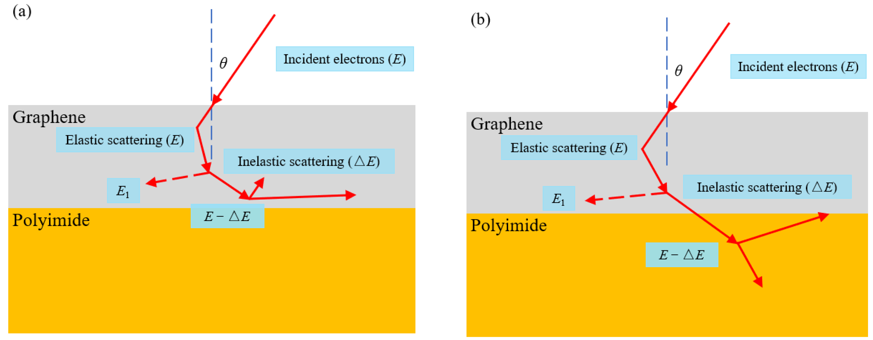
3.1. SEY and Theoretical Analysis

During the SEY test of the materials, the graphene coating was found to have a significant inhibitory effect on the secondary electron emissions of polyimide materials. The graphene coating was placed on the uppermost side of the sample stage during the test. The SEY test results of the materials were shown in Figure 3. Figure 3 illustrated that the SEY of polyimide materials showed a tendency to increase and then decrease, and there was a maximum value (δmax) of 1.72. The SEY of the polyimide materials had a peak of 1.72 with an incident electron energy of 100 eV. It can be seen that the SEY curves after deposition of graphene coatings with different layers by CVD showed the same trend of increasing and then decreasing. The polyimide materials with three layers of graphene coating had an incident electron energy of 200 eV with a peak of 1.52. Therefore, the maximum SEY (δmax) was reduced by 12%. It can be noted that the graphene coating had a better inhibition effect on polyimide materials at low energy incident electron incidences. The one-layer graphene coating had the best inhibitory effect at high energy incident electron incidences. All three different layers of the graphene coatings shifted the SEY curves peak of the polyimide materials backward and reduced it significantly. The smaller the peak of the SEY, the better the stability of the device under electron vacuum equipment and space working conditions. The smaller SEY peak of the materials was necessary. It can also be concluded from Figure 3 that the SEY curves of polyimide materials with different thicknesses of graphene coating were different. This may be attributed to the difference in the thickness of the graphene coating. The results showed that the graphene coating was an excellent coating for polyimide materials to suppress secondary electron emissions. The two-layer graphene coating was selected for surface morphology analysis after comprehensive consideration.
This paper theoretically analyzes the effect of graphene coating on secondary electron emissions from polyimide materials. The process of secondary electron emission is that the incident electrons excite the electrons inside the material, causing them to jump and produce secondary electrons. When the secondary electrons move without direction in the material, they are scattered by the free electrons in the material, and the energy gradually decays with the distance increase [33,34]. Secondary electrons within a certain distance from the material surface move towards the material surface. When they move to the surface of the material, the secondary electrons escape into the vacuum with a higher energy than the escape function of the material in order to complete the escape. Generally, the energy of the secondary electrons escaping into the vacuum is less than 50 eV. Therefore, only the secondary electrons that are excited within a certain depth of the surface of the material and have sufficient energy can move to the surface of the material and escape into the vacuum.
Graphene coatings have an effect on both primary and secondary electrons [27]. The principle of the graphene coating affecting secondary electrons is shown in Figure 4. The distance between carbon atoms in the graphene coating is about 0.142 nm, and the distance between carbon atoms in a polyimide substrate is about 0.15 nm. It is very difficult for the incident electrons to penetrate the dense atomic layer. Therefore, in the presence of a graphene coating, fewer of the incident electrons can actually enter the polyimide substrate, and fewer internal electrons can be excited within it, which is one of the reasons that the graphene coating suppresses secondary electron emissions. Another more important effect of graphene coatings is on internal secondary electron emissions [35]. After the incident electrons enter the graphene coating, inelastic scattering occurs, losing some of the electron energy and generating some internal secondary electron scattering [25]. The secondary electrons with some energy will be further scattered until their energy is exhausted. Eventually, some scattered secondary electrons can reach the surface. For polyimide materials without a graphene coating, the emission of internal secondary electrons only needs to pass through the surface barrier. However, if the surface is covered by graphene, the internal secondary electrons must penetrate further through the graphene for effective emission. The effect of a graphene coating on secondary electrons is more complex than the primary electrons [36].
The energy of most internal secondary electrons is a few eV, which is much lower than the incident electrons [1]. It is more difficult for low-energy electrons to penetrate the graphene coating than high-energy electrons, and this is also related to the angle of incident electrons. After incidence of the primary electrons at different angles, the internal secondary electrons have a certain direction distribution. Only a part of the internal secondary electrons with high energy can emit secondary electrons. The effective potential barrier can be described as the effect of graphene coating on the emission of internal secondary electrons.

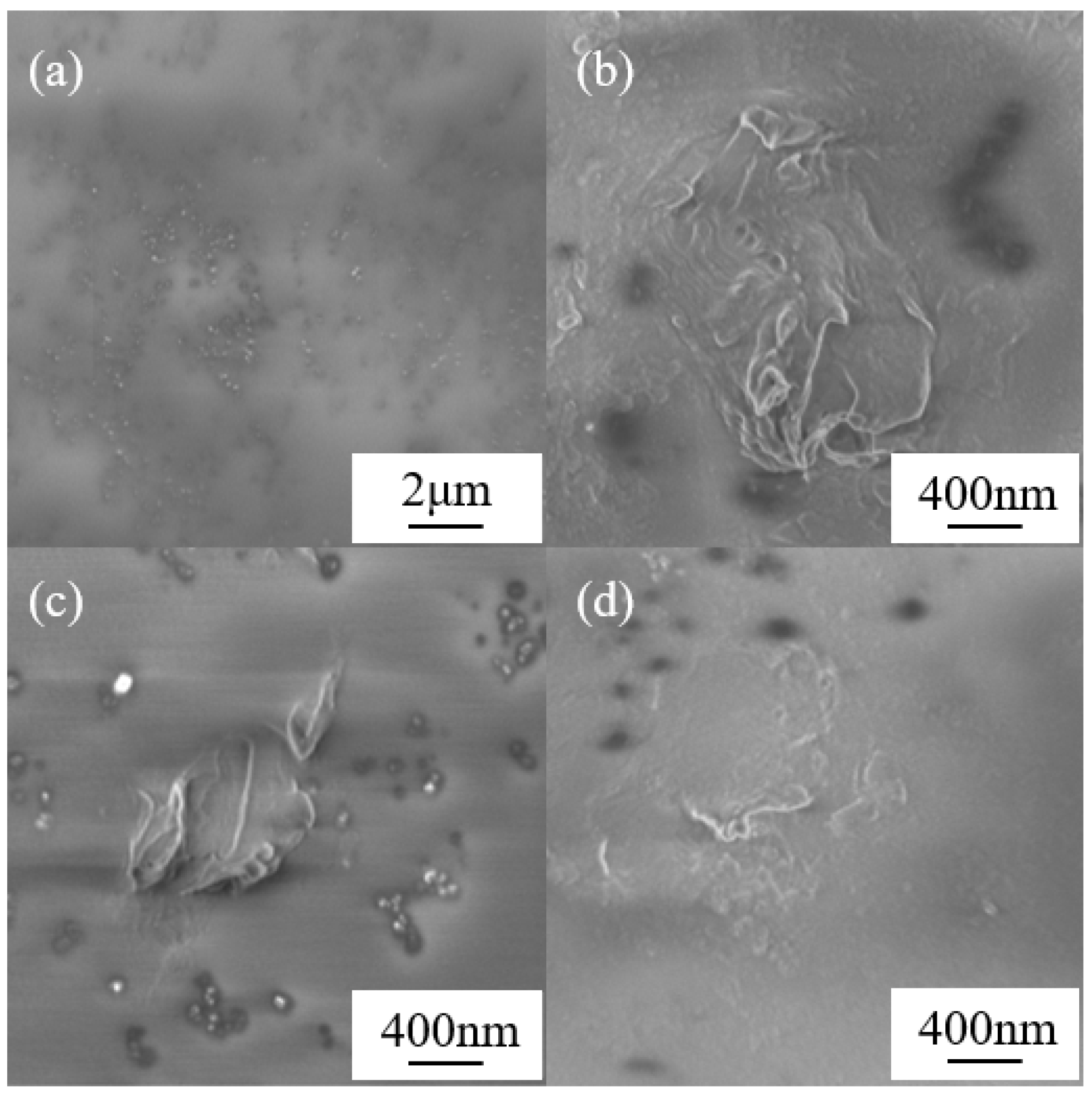
3.2. Surface Morphology Study of the Graphene-Coated Polyimide Materials

The graphene-coated polyimide materials were fabricated using the CVD method. Graphene-coated samples with different thicknesses (1, 2, and 3 layers) were prepared. The fabrication process was shown in Figure 1. The process of the material preparation was detailed in Section 2.1. According to Figure 3, it was clear that the two-layer graphene coating was chosen for material characterization due to its moderate SEY. The SEM image of graphene-coated polyimide materials (as an example of two-layer graphene coating) was shown in Figure 5, which showed the surface topography of the graphene-coated polyimide materials. The SEM enlargement image of graphene-coated polyimide materials from three different locations was shown in Figure 5b–d. The thickness can be derived from the AFM analysis. It can be observed that the graphene coating clearly had very thin, wrinkled, and rolled morphologies, indicating that the small number of layers of the structure was present. This indicates that the graphene coating was successfully prepared on the polyimide surface using the CVD method. It can also be observed that there were some obvious protrusions on the surface of the polyimide substrate, which is due to the rich organic surface of the polyimide material. This may be one of the reasons affecting the secondary electron emission of the material. It is worth noting that the adhesion between the polyimide substrate and the graphene coating was quite strong, which was due to the fact that the graphene particles on the surface were partially embedded in the substrate [34,35]. Therefore, the graphene-coated polyimide film materials were successfully prepared using this CVD method.
The samples were analyzed by XPS [37]. Figure 6a shows the XPS full spectrum curve of the tested sample. It can be observed that the main peaks in the spectrum curve were dominated by C1s, O1s, and N1s. The energy loss peaks near the main peaks of C1s and O1s were found. This is because of the photoelectrons losing a certain amount energy in the process of leaving the sample surface by interacting with other electrons on the surface. Consequently, some companion peaks are on the low kinetic energy side of the XPS spectroscopy [38]. Figure 6a illustrated that the tested samples were mainly C, O, and N elements, which occupied 65.85, 20.47, and 13.68 at.%, respectively. From the comparison of polyimide and graphene XPS data in the literature, it can be seen that the intensity of the main peak of C1s was increased, indicating that the graphene coating had been prepared on this polyimide substrate.
In order to further understand the functional group content on the surface of the graphene-coated polyimide material [39,40], the C1s and O1s XPS fine spectra of the tested sample were analyzed. Figure 6b showed the C1s fine spectrum of the tested samples, which showed the characteristics of C1s and energy loss. It can be seen that the tested samples contained abundant sp2 and sp3 heterostructures, as well as abundant hydroxyl and epoxy groups. Figure 6c showed the fine spectrum of O1s of the tested samples, which can be seen to exist mainly as carbon–oxygen single and double bonds. The analysis of the O1s fine spectra curve fully supported these findings. According to the literature, the sp2 hybridized structure reduced the SEY of the material. This is the main reason for reducing the SEY of the material. According to Section 3.1, the SEY of the polyimide material can be reduced to 1.52.
In order to suppress the secondary electron emissions, the abundant sp2 hybridized structure in the tested material was necessary. XPS analysis showed that the carbon atoms in the tested material were still dominated by sp2 and sp3 hybridization. In order to further analyze the chemical composition and structure of the tested samples, Raman analysis of the tested material was performed.
According to the generation principle of Raman spectroscopy, the materials with different atomic structures produce different Raman characteristic peaks due to the different shapes of the electron cloud and the scattering of excited electron and phonon interactions [41]. In this study, three random locations on the coating surface were selected for Raman spectral analysis (A, B, and C). Figure 7a shows the Raman spectra of the three locations on the surface of the tested sample, which can show that the coating structure was uniform and stable. The Raman spectral peak fitting was performed as shown in Figure 7b.
In the Raman spectrum of graphene-coated polyimide, the characteristic G and D bands of graphitic materials were typically observed at Raman shifts around 1600 cm−1 and 1400 cm−1, respectively. IG/ID was the intensity ratio between the high-frequency peak (G bands) and the low-frequency peak (D bands). In Figure 7b, the intensity of the G bands was significantly lower than that of the D bands. When the intensity of the D bands in a material is significantly higher than that of the G bands, it usually indicates the presence of more structural defects or incompleteness, and may also indicate the presence of more layers of graphene. It may lead to a change in the layer spacing of the graphite material when the number of layers is high, thus affecting the G bands strength of the materials. However, due to the thin graphene coating of the graphene-coated polyimide, the ratio reflected the nature of the overall material, which was due to the fact that the surface of the polyimide material had defects or was incomplete. This is due to the fact that polyimide is a polymer polymerization material.
According to the literature, it is known that graphene has a structure such as sp2 hybridization, which has a characteristic peak (G peak) near the Raman shift of 1580 cm−1. The G peak is the plane vibration spectrum of the six rings in a two-dimensional plane. It can be seen that the tested sample had a strong G peak with a slight slip. The slight slip in the position of the split peak may be caused by intermaterial interactions after preparing the graphene coating. The G peak indicated that the carbon atoms in the tested sample had an sp2 hybridized structure. Meanwhile, according to the comparison of polyimide spectral data, it can be seen that the polyimide also has a hexacyclic structure and produced characteristic peaks near the Raman shift of 1200 cm−1. This may be due to the environmental factors of the test instrument. It can also be concluded from the Raman spectral analysis that the structure of the tested sample is an abundant sp2 hybridized structure, which was consistent with the conclusion of the XPS analysis of the C1s XPS fine spectra curve.
Figure 8 shows the AFM morphology of the tested samples at different locations with different resolutions. The surface roughness of the polyimide substrate was altered due to the preparation of graphene coatings by chemical vapor deposition. Therefore, the surface roughness and uniformity of the prepared graphene-coated polyimide material were analyzed by AFM.
Different locations with different resolutions were selected for AFM analysis [42,43]. Figure 8a shows the AFM image of the prepared graphene-coated polyimide material, and Figure 8b shows the 3D morphology of it. Four different locations (A, B, C, and D) were selected along the material. The surface height curves under the selected paths after smoothing were shown in Figure 8e. It can be found that the surface heights were basically the same, and mostly within the range of 2 nm. At the same time, it can be noticed that A was slightly higher compared to BCD. According to Figure 8a, this is caused by the particles of the polyimide polymer material. It can be seen that the surface of the material was basically homogeneous, and the roughness is 0.865 nm at this location. For further validation and analysis, high-resolution AFM analysis was performed. Figure 8c shows the high-resolution AFM image of the prepared graphene-coated polyimide material, and Figure 8d shows the high-resolution 3D morphology of the prepared graphene-coated polyimide material. On this basis, four different locations (E, F, G, and H) were selected along the material direction. The surface height curves under the selected paths were smoothed and processed as shown in Figure 8f.
It can be found that the surface heights were basically the same, and it is verified that the surface of the material was basically homogeneous. The thicknesses of the materials were within a range of 2 nm, and the roughness of the materials at this position is 0.619 nm. The material preparation requirements within the error tolerance can be met. Meanwhile, the graphene coating surface prepared using the CVD method was uniform, and its coating surface height variation range was between 2~4 nm. The experimental results can meet the requirements of suppressing secondary electron emissions.

3.3. Discussion

Polyimide materials were insulating materials, and their secondary electron emissions need to overcome the potential surface barriers of the materials. Due to polyimide materials being a polymer polymerization material, the surface morphology was complex, and the surface morphology after the preparation of a graphene coating was also complex. Only cursory observations could be made from SEM images, and elemental analyses were carried out using a variety of characterization methods. More delicate methods will be used to characterize the materials in future studies. According to the researchers, the coating thickness was an important factor affecting the secondary electron emissions from the surface of the materials, so the effect of the graphene coating thickness on the surface of the polyimide materials was also critical. In this paper, the effect of three graphene coating thicknesses on the secondary electrons of polyimide materials was investigated. Subsequently, the Monte Carlo numerical simulation method can be used to analyze the effect of graphene coating thickness on polyimide materials, and explore the thickness of the graphene coating with lower secondary electron emission yields. Meanwhile, the specific parameters of the CVD process were mainly used to prepare graphene coating materials with different thicknesses. Temperature, humidity, and time in the environment may also affect the performance of the coating materials, the main reason may be to affect the surface morphology of the material to affect the secondary electron emission yield; stability tests can be conducted for these factors in future studies to investigate the effect of this coating on the stability of polyimide materials.

4. Conclusions

The graphene coatings on polyimide surfaces were prepared using CVD methods, and the SEY was tested by a secondary electron measurement device. The changes of functional groups and the structure of carbon atoms in the graphene coating of the tested samples were analyzed. The deposited graphene coating was uniformly grown on the surface of the polyimide materials. The XPS results showed that the C, O, and N contents in the tested samples were 65.85, 20.47, and 13.68 at.%, respectively. The tested sample still maintained the abundant sp2 hybridized structure. According to the Raman spectra analysis, it can be seen that the defects were reduced compared to the polyimide, and the analytical results were consistent with the XPS analysis. The SEY (δmax) of the polyimide materials with the graphene coating decreased from 1.72 to 1.52, which indicated that the graphene coating had a good suppression effect on the secondary electron emissions of the polyimide materials. This is because most of the carbon atoms in the graphene coating maintained the abundant sp2 hybridized structure. In addition, the CVD methods offered simple equipment, ease of operation, and greater flexibility than other preparation methods. This study can provide new ideas for the study of polyimide materials in aerospace and particle gas pedals for suppressing secondary electron emissions.

Author Contributions

X.Q.: Conceptualization, Methodology, Validation, Formal analysis, Investigation, Data curation, Writing—original draft. Y.M.: Conceptualization, Methodology, Investigation, Supervision, Project administration, Funding acquisition. S.L.: Investigation, Validation, Supervision. T.Z.: Resources, Validation, Supervision. X.N.: Resources, Supervision. Y.W.: Investigation, Data curation. W.P.: Resources, Supervision. G.H.: Conceptualization, Supervision, Project administration. All authors have read and agreed to the published version of the manuscript.

Funding

This research was funded by the Aerospace Science and Technology Group Applied Innovation Program, grant number 6230114001, and Reliability and Environmental Engineering Technology Key Laboratory Fund Program, grant number 6142004210201.

Institutional Review Board Statement

Not applicable.

Informed Consent Statement

Not applicable.

Data Availability Statement

The data presented in this study are available on request from the corresponding author.

Conflicts of Interest

The authors declare no conflict of interest.

Correction Statement

This article has been republished with a minor correction to the existing affiliation information (aff. 3 should be Wuhan Second Ship Design and Research Institute, Wuhan 430205, China). This change does not affect the scientific content of the article.

References

  1. Kong, F.; Zhang, P.H.; Yu, W.X.; Zhang, C.; Liu, J.B.; Ren, C.Y.; Shao, T. Enhanced surface insulating performance for polystyrene by atmospheric pressure plasma jet deposition. Appl. Surf. Sci. 2020, 527, 146826. [Google Scholar] [CrossRef]
  2. Wang, D.; He, Y.N.; Cui, W.Z. Secondary electron emission characteristics of TiN coatings produced by RF magnetron sputtering. J. Appl. Phys. 2018, 124, 053301. [Google Scholar] [CrossRef]
  3. Santos, A.; Bundaleski, N.; Shaw, B.J.; Silva, A.G.; Teodoro, O. Increase of secondary electron yield of amorphous carbon coatings under high vacuum conditions. Vacuum 2013, 98, 37–40. [Google Scholar] [CrossRef]
  4. Lapington, J.S.; Thompson, D.P.; May, P.W.; Fox, N.A.; Howorth, J.; Milnes, J.; Taillandier, V. Investigation of the secondary emission characteristics of CVD diamond films for electron amplification. Nucl. Instrum. Methods Phys. Res. Sect. A Accel. Spectrometers Detect. Assoc. Equip. 2009, 610, 253–257. [Google Scholar] [CrossRef]
  5. Costin, C. Secondary electron emission under magnetic constraint: From Monte Carlo simulations to analytical solution. Sci. Rep. 2021, 11, 1874. [Google Scholar] [CrossRef]
  6. Liu, X.W.; Mang, G.J.; Li, J.; Shi, G.L.; Zhou, M.Y.; Huang, B.Q.; Tang, Y.J.; Song, X.H.; Yang, W.F. Deep Learning for Feynman’s Path Integral in Strong-Field Time-Dependent Dynamics. Phys. Rev. Lett. 2020, 124, 113202. [Google Scholar] [CrossRef]
  7. Raitses, Y.; Kaganovich, I.D.; Khrabrov, A.; Sydorenko, D.; Fisch, N.J.; Smolyakov, A. Effect of Secondary Electron Emission on Electron Cross-Field Current in E x B Discharges. IEEE Trans. Plasma Sci. 2011, 39, 995–1006. [Google Scholar] [CrossRef]
  8. Liu, L.; Meng, X.N.; Miao, Z.; Zhou, S. Design of a novel thermoelectric module based on application stability and power generation. Case Stud. Therm. Eng. 2022, 31, 101836. [Google Scholar] [CrossRef]
  9. Choi, H.J.; Jung, S.M.; Seo, J.M.; Chang, D.W.; Dai, L.M.; Baek, J.B. Graphene for energy conversion and storage in fuel cells and supercapacitors. Nano Energy 2012, 1, 534–551. [Google Scholar] [CrossRef]
  10. Ma, J.Z.; Wei, L.F.; Bai, Y.R.; Bao, Y.; Kang, Q.L.; Zhang, W.B.; Cui, W.Z.; Hu, T.C.; Wu, D.D. Controllable preparation of silver nano-bowl coatings for suppressing secondary electron emission. Thin Solid Film. 2021, 725, 138633. [Google Scholar] [CrossRef]
  11. Wang, J.; Gao, Y.; You, Z.M.; Fan, J.K.; Zhang, J.; Wang, S.; Xu, Z.L. Laser Induced Nano and Micro Structures of Molybdenum Surface Applied in Multistage Depressed Collector for Secondary Electron Suppression. Appl. Sci. 2019, 9, 4374. [Google Scholar] [CrossRef]
  12. Swanson, C.; Kaganovich, I.D. Modeling of reduced secondary electron emission yield from a foam or fuzz surface. J. Appl. Phys. 2018, 123, 023302. [Google Scholar] [CrossRef]
  13. Cimino, R.; Commisso, M.; Grosso, D.R.; Demma, T.; Baglin, V.; Flammini, R.; Larciprete, R. Nature of the Decrease of the Secondary-Electron Yield by Electron Bombardment and its Energy Dependence. Phys. Rev. Lett. 2012, 109, 064801. [Google Scholar] [CrossRef] [PubMed]
  14. Pivi, M.; King, F.K.; Kirby, R.E.; Raubenheimer, T.O.; Stupakov, G.; Le Pimpec, F. Sharp reduction of the secondary electron emission yield from grooved surfaces. J. Appl. Phys. 2008, 104, 104904. [Google Scholar] [CrossRef]
  15. Liu, L.; Feng, G.B.; Chen, B.D.; Wang, N.; Cui, W.Z. Characteristics of secondary electron emission and multipactor from a nested microtrap structure surface. AIP Adv. 2021, 11, 025332. [Google Scholar] [CrossRef]
  16. Zhang, Y.X.; Wang, Y.G.; Wang, S.H.; Wei, W.; Ge, X.Q.; Zhu, B.L.; Shao, J.Q.; Wang, Y. Comparison of Carbon Thin Films with Low Secondary Electron Yield Deposited in Neon and Argon. Coatings 2020, 10, 884. [Google Scholar] [CrossRef]
  17. Wang, G.D.; Liu, D.M.; Fan, S.Q.; Li, Z.Y.; Su, J. High-k erbium oxide film prepared by sol-gel method for low-voltage thin-film transistor. Nanotechnology 2021, 32, 215202. [Google Scholar] [CrossRef]
  18. Nivas, J.J.J.; Valadan, M.; Salvatore, M.; Fittipaldi, R.; Himmerlich, M.; Rimoldi, M.; Passarelli, A.; Allahyari, E.; Oscurato, S.L.; Vecchione, A.; et al. Secondary electron yield reduction by femtosecond pulse laser-induced periodic surface structuring. Surf. Interfaces 2021, 25, 101179. [Google Scholar] [CrossRef]
  19. Jo, G.; Choe, M.; Lee, S.; Park, W.; Kahng, Y.H.; Lee, T. The application of graphene as electrodes in electrical and optical devices. Nanotechnology 2012, 23, 112001. [Google Scholar] [CrossRef]
  20. Park, J.H.; Park, J.M. Electrophoretic deposition of graphene oxide on mild carbon steel for anti-corrosion application. Surf. Coat. Technol. 2014, 254, 167–174. [Google Scholar] [CrossRef]
  21. Tang, H.C.; Yang, C.; Lin, Z.Y.; Yang, Q.H.; Kang, F.Y.; Wong, C.P. Electrospray-deposition of graphene electrodes: A simple technique to build high-performance supercapacitors. Nanoscale 2015, 7, 9133–9139. [Google Scholar] [CrossRef] [PubMed]
  22. Pavithra, C.L.P.; Sarada, B.V.; Rajulapati, K.V.; Rao, T.N.; Sundararajan, G. A New Electrochemical Approach for the Synthesis of Copper-Graphene Nanocomposite Foils with High Hardness. Sci. Rep. 2014, 4, 4049. [Google Scholar] [CrossRef] [PubMed]
  23. Geng, D.S.; Yang, S.L.; Zhang, Y.; Yang, J.L.; Liu, J.; Li, R.Y.; Sham, T.K.; Sun, X.L.; Ye, S.Y.; Knights, S. Nitrogen doping effects on the structure of graphene. Appl. Surf. Sci. 2011, 257, 9193–9198. [Google Scholar] [CrossRef]
  24. Mai, Y.J.; Zhou, M.P.; Ling, H.J.; Chen, F.X.; Lian, W.Q.; Jie, X.H. Surfactant-free electrodeposition of reduced graphene oxide/copper composite coatings with enhanced wear resistance. Appl. Surf. Sci. 2018, 433, 232–239. [Google Scholar] [CrossRef]
  25. Larciprete, R.; Grosso, D.R.; Di Trolio, A.; Cimino, R. Evolution of the secondary electron emission during the graphitization of thin C films. Appl. Surf. Sci. 2015, 328, 356–360. [Google Scholar] [CrossRef]
  26. Cao, M.; Zhang, X.S.; Liu, W.H.; Wang, H.G.; Li, Y.D. Secondary electron emission of graphene-coated copper. Diam. Relat. Mater. 2017, 73, 199–203. [Google Scholar] [CrossRef]
  27. Wang, J.; Wang, Y.; Xu, Y.H.; Zhang, Y.X.; Zhang, B.; Wei, W. Secondary electron emission characteristics of graphene films with copper substrate. Chin. Phys. C 2016, 40, 117003. [Google Scholar] [CrossRef]
  28. Sian, T.; Lin, Y.; Valizadeh, R.; Malyshev, O.B.; Xia, G.; Valles, C.; Yu, G.; Kinloch, I. Graphene coating for the reduction of the secondary electron yield. Proc. IPAC 2016, 2, 3688–3690. [Google Scholar]
  29. Aguincha, R.; Bundaleski, N.; Bundaleska, N.; Novakovi, M.; Teodoro, O. Low total electron yield graphene coatings produced by electrophoretic deposition. Appl. Surf. Sci. 2019, 504, 143870. [Google Scholar] [CrossRef]
  30. Luo, J.; Tian, P.; Pan, C.T.; Robertson, A.W.; Warner, J.H.; Hill, E.W.; Briggs, G. Ultralow Secondary Electron Emission of Graphene. ACS Nano 2011, 5, 1047. [Google Scholar] [CrossRef]
  31. Bundaleski, N.; Belhaj, M.; Gineste, T.; Teodoro, O. Calculation of the angular dependence of the total electron yield. Vacuum 2015, 122, 255–259. [Google Scholar] [CrossRef]
  32. Nguyen, H.K.A.; Mankowski, J.; Dickens, J.C.; Neuber, A.A.; Joshi, R.P. Calculations of secondary electron yield of graphene coated copper for vacuum electronic applications. AIP Adv. 2018, 8, 015325. [Google Scholar] [CrossRef]
  33. Fernandez, H.M.; Himmerlich, M.; Pinto, P.C.; Coroa, J.; Sousa, D.; Baris, A.; Taborelli, M. The impact of H-2 and N-2 on the material properties and secondary electron yield of sputtered amorphous carbon films for anti-multipacting applications. Appl. Surf. Sci. 2021, 542, 148552. [Google Scholar] [CrossRef]
  34. Fitting, H.J.; Touzin, M. Time-dependent start-up and decay of secondary electron emission in dielectrics. J. Appl. Phys. 2010, 108, 033711. [Google Scholar] [CrossRef]
  35. Tatarova, E.; Dias, A.; Henriques, J.; Abrashev, M.; Bundaleska, N.; Kovacevic, E.; Bundaleski, N.; Cvelbar, U.; Valcheva, E.; Arnaudov, B.; et al. Towards large-scale in free-standing graphene and N-graphene sheets. Sci. Rep. 2017, 7, 10175. [Google Scholar] [CrossRef]
  36. Montero, I.; Aguilera, L.; Davila, M.E.; Nistor, V.C.; Gonzalez, L.A.; Galan, L.; Raboso, D.; Ferritto, R. Secondary electron emission under electron bombardment from graphene nanoplatelets. Appl. Surf. Sci. 2014, 291, 74–77. [Google Scholar] [CrossRef]
  37. Zhang, W.H.; Nefedov, A.; Naboka, M.; Cao, L.; Woll, C. Molecular orientation of terephthalic acid assembly on epitaxial graphene: NEXAFS and XPS study. Phys. Chem. Chem. Phys. 2012, 14, 10125–10131. [Google Scholar] [CrossRef]
  38. Biesinger, M.C.; Lau, L.W.M.; Gerson, A.R.; Smart, R.S.C. Resolving surface chemical states in XPS analysis of first row transition metals, oxides and hydroxides: Sc, Ti, V, Cu and Zn. Appl. Surf. Sci. 2010, 257, 887–898. [Google Scholar] [CrossRef]
  39. Kadari, A.; Schemme, T.; Kadri, D.; Wollschlager, J. XPS and morphological properties of Cr2O3 thin films grown by thermal evaporation method. Results Phys. 2017, 7, 3124–3129. [Google Scholar] [CrossRef]
  40. Jung, R.H.; Tsuchiya, H.; Fujimoto, S. XPS characterization of passive films formed on Type 304 stainless steel in humid atmosphere. Corros. Sci. 2012, 58, 62–68. [Google Scholar] [CrossRef]
  41. Yang, X.; Sun, G.Y.; Zhou, R.D.; Huang, K.; Li, W.D.; Wang, C.; Dong, J.F.; Song, B.P.; Zhang, G.J. Ultralow secondary electron emission and improved vacuum surface insulation of polyimide with scalable nanocomposite coating. Appl. Surf. Sci. 2022, 592, 153221. [Google Scholar] [CrossRef]
  42. Zhang, H.F.; Ge, Y.; Pan, P.; Du, Y.H.; Fu, H.; Yan, M.J.; Li, P.; Long, H.M.; Zhang, C.Z.; Cai, J.; et al. Suppression of secondary electron emission on oxygen-free copper surface of reduced graphene oxide coatings prepared by electrophoretic deposition. Appl. Surf. Sci. 2022, 603, 1544900. [Google Scholar] [CrossRef]
  43. Lu, Q.; Yu, B.; Hu, Z.Q.; He, Y.; Hu, T.C.; Zhao, Y.N.; Wang, Z.G.; Zhou, Z.Y.; Cui, W.; Liu, M. Surface roughness evolution induced low secondary electron yield in carbon coated Ag/Al substrates for space microwave devices. Appl. Surf. Sci. 2020, 501, 144236. [Google Scholar] [CrossRef]
Figure 1. The preparation flow of the polyimide graphene coating preparation by CVD method.
Coatings 13 01805 g001
Figure 2. (a) is the secondary electron measurement device, (b) is the principle of the secondary electron measurement.
Coatings 13 01805 g002
Figure 3. SEY of the polyimide materials.
Coatings 13 01805 g003
Figure 4. The schematic diagram of graphene coating affecting secondary electrons. (a) The internal electron not entering polyimide substrate; (b) The internal electrons entering the polyimide substrate.
Coatings 13 01805 g004
Figure 5. (a): The SEM images depict the prepared graphene-coated polyimide materials. (bd): The SEM images depict the prepared graphene-coated polyimide materials at different positions.
Coatings 13 01805 g005
Figure 6. (a) is the XPS full spectrum curve of the prepared graphene-coated polyimide material, (b) is the C1s XPS fine spectra curve, (c) is the O1s XPS fine spectra curve.
Coatings 13 01805 g006
Figure 7. Raman spectral of the prepared graphene-coated polyimide material. (a) Raman spectra of the materials at A, B, and C; (b) the fitted curve of Raman spectra at A.
Coatings 13 01805 g007
Figure 8. (a) is the AFM image of the prepared graphene-coated polyimide material, (b) is the 3D topography of Figure 8a, (c) is the high-resolution AFM image of the prepared graphene-coated polyimide material, (d) is the 3D topography of (c), (e) is the surface height curve under the selected paths of (a), and (f) is the surface height curve under the selected paths of (c).
Coatings 13 01805 g008
Disclaimer/Publisher’s Note: The statements, opinions and data contained in all publications are solely those of the individual author(s) and contributor(s) and not of MDPI and/or the editor(s). MDPI and/or the editor(s) disclaim responsibility for any injury to people or property resulting from any ideas, methods, instructions or products referred to in the content.

