
Numerical Investigation on the Effect of Electrical Parameters on the Discharge Characteristics of NS-SDBD

1
School of Aeronautics, Chongqing Jiaotong University, Chongqing 400074, China
2
Chongqing Key Laboratory of Green Aviation Energy and Power, The Green Aerotechnics Research Institute of Chongqing Jiaotong University, Chongqing 401120, China
3
School of Automation and Information Engineering, Xi’an University of Technology, Xi’an 710048, China
*
Author to whom correspondence should be addressed.
Coatings 2023, 13(7), 1237; https://doi.org/10.3390/coatings13071237
Submission received: 8 June 2023
/
Revised: 3 July 2023
/
Accepted: 8 July 2023
/
Published: 11 July 2023
(This article belongs to the Topic Modeling, Fabrication, and Characterization of Semiconductor Materials and Devices)
Abstract
:There are numerous scientific and engineering fields where the surface dielectric barrier discharge driven by nanosecond pulses (NS-SDBD) has important applications. To improve its performance, more research is still needed on the effects of electrical parameters on the NS-SDBD actuator’s discharge characteristics. In this study, a two-dimensional numerical model based on 13 discharge particle chemical processes was constructed using a numerical simulation approach, producing findings for the NS-SDBD actuator’s voltage–current (V-A) characteristics, discharge profile, and spectrum analysis. Additionally, a comprehensive investigation into the trends and underlying mechanisms of the effects of the voltage amplitude, pulse width, rise time, and fall time parameters on the discharge behavior of the NS-SDBD actuator was carried out. The results show that higher voltage amplitudes increase the maximum current and electron density, which enhances the plasma excitation effect. The peak power deposition during the second discharge is also raised by longer pulse widths and rise times, whereas the total power deposition during the second discharge is decreased by longer fall times.
1. Introduction
Numerous scientific and engineering fields apply plasma in various ways, and due to its tiny size, light weight, and great efficiency, the surface dielectric barrier discharge generated by nanosecond pulses (NS-SDBD) has attracted the most attention. The NS-SDBD actuator can generate plasma under atmospheric conditions, and due to the significant application value of plasma, it has been widely used in material surface modification [1], coating [2], environmental treatment [3], biomedicine [4], icing control [5], and fluid control [6] and other fields.
A growing number of research has focused on the impact of electrical factors on the NS-SDBD’s discharge characteristics as a result of the rapid improvement of nanosecond pulsed power supply technology in recent years [7]. Voltage amplitude, pulse width, rise time, and fall time are among the factors that have a big impact on the NS-SDBD actuator’s discharge characteristics. The NS-SDBD actuator’s potential application areas can be expanded by the precise rate control and optimization of these factors, which can also increase the discharge efficacy and energy economy.
In an effort to improve the NS-SDBD actuator discharge effect and boost energy utilization, a number of researchers have conducted experimental research and examined the impact of electrical factors on the discharge characteristics of NS-SDBD. Benard et al. [8] investigated how electrode polarity and pulse width time affected discharge characteristics and found that positive pulses cause more energy deposition than negative pulses. The effects of voltage amplitude and electrode polarity on the discharge characteristics of NS-SDBD were investigated by Lei et al. [9], and the results showed that the energy deposition of positive pulses would exceed that of negative pulses, and the discharge would be more uniform. Xie et al. [10] investigated the effect of the rise time on the discharge characteristics of the NS-SDBD actuator and discovered that a shorter rise time results in a larger starting vortex. Huang et al. [11] investigated the spatial distribution and temporal evolution of the NS-SDBD actuator’s electric field with pulse repetition frequency. Due to experimental method restrictions, a full examination of the physical discharge process of the NS-SDBD actuator could not be performed in these tests. Additionally, the NS-SDBD plasma excitation disturbances’ time and spatial dimensions are extremely small, requiring high accurate measuring tools and rather expensive experimental expenditures. Therefore, research on the discharge characteristics of NS-SDBD actuators has grown dependent on numerical modeling.
Focusing on the numerical simulation of plasma, computational methods such as the Monte Carlo model [12], fluid model [13,14,15], and particle-in-cell (PIC) model [16] have mainly been developed. The fluid model might identify the primary physical processes in the discharge process when simulating the discharge characteristics of the NS-SDBD actuator. The plasma fluid model has been the subject of much numerical investigation by many academics. Soloviev et al. [17] investigated the effect of electrode polarity on the NS-SDBD discharge process, and the results revealed that the current waveforms were consistent for both polarity pulse voltages. Ahn et al. [18] investigated the discharge process of an NS-SDBD actuator and discovered that the electron energy and physical parameters of the electric field can vary for different regions of plasma formation. Shi et al. [19] investigated the physical process of SDBD discharge under various voltage amplitudes and frequencies, and the results revealed that the voltage amplitude and frequency increase the discharge current. The effect of pulse repetition frequency on the residual surface charge of NS-SDBD was investigated by Peng et al. [20]. The influence of the rise time on the discharge characteristics of NS-SDBD was investigated by Xu et al. [21], and the results revealed that the shorter the rise time, the greater the discharge intensity and discharge area.
The investigation into how electrical parameters affect the discharge characteristics of NS-SDBD has made some progress. Some researchers have concentrated on how specific parameters affect discharge behavior, such as how voltage amplitude affects the intensity of the discharge and how the rise time affects the duration of the discharge. However, few studies have considered the comprehensive influence of multiple electrical parameters on discharge characteristics, thus limiting us from gaining a deeper understanding of the discharge mechanism of the NS-SDBD actuator. By using numerical simulation methods, this work seeks to comprehensively evaluate the impacts of electrical parameters on the discharge characteristics of the NS-SDBD actuator and to further explore the influence mechanism of the effects of parameter variations on the discharge behavior. In the following investigation, a number of variables are taken into account, and their impacts on the discharge current, electron density, and total power deposition are quantitatively studied. These variables include the voltage amplitude, pulse width, rise time, and fall time.
2. Numerical modeling
2.1. Plasma Fluid Model
In order to study the influence of nanosecond pulse electrical parameters on the discharge characteristics of the NS-SDBD, a two-dimensional asymmetric fluid model was constructed in this study. The model solves the continuity equations, electron energy conservation equation, momentum conservation equation, and Poisson’s equation to obtain the spatiotemporal distributions of key parameters during the plasma discharge process and help us gain a deep understanding of the discharge characteristics and physical mechanisms of NS-SDBD actuators.
The particle number density of electrons and ions are obtained by solving the continuity equation:
In the equation, represents the number of particles per unit volume; is the vector electric field strength; and are the particle diffusion coefficient and particle mobility, respectively, which describe the particle spatial characteristics; is the particle charge number (equal to −1 for electrons and negative ions, 0 for neutral particles, and +1 for positive ions); and represents the particle source term caused by reactions such as electron collisions, molecule and atom collisions, etc. The specific formula is as follows:
In the equation, is the reaction rate coefficient composed of the monomolecular reaction rate coefficient, bimolecular reaction rate coefficient, and trimolecular reaction rate coefficient; and and are the Townsend coefficient and electron flux for particle reactions, respectively.
Electron energy is a key parameter that determines the drift-diffusion velocity of electrons and the chemical reaction rate, which have a significant impact on the discharge morphology. The electron temperature is solved by the following equation:
In the equation, and represent the electron density and average electron energy, respectively, and represents the flux of electron energy. The calculation formula is as follows:
In the equation, and represent the electron energy mobility and electron energy diffusion coefficient, respectively, and their calculation formulas are as follows:
Here, the mobility and diffusion coefficient satisfy the Einstein relationship:
Here, represents Boltzmann constant (1.38 × 10⁻²³ J·K–1), and represents elementary positive charge (1.6 × 10⁻¹⁹ C).
In Equation (3), the electron energy source term, , is as follows:
Here, represents the energy threshold (eV) of particle collision reactions.
The combined effects and interactions between the Laplace electric field and the space charge electric field determine the distribution and strength of the electric field during the discharge process. The Laplace electric field is generated by the potential difference between the electrodes and formed between the electrodes. It mainly distributes along the straight path between the electrodes and plays a major driving role in the discharge process by pushing electrons and ions to move in space. The electric field generated by space charges is caused by the spatial distribution of electrons and ions during the discharge and is non-uniformly distributed in the discharge area, with its intensity varying with the spatial charge density. The electric field and electric potential are solved by the Poisson equation:
In the equation, and are the vacuum permittivity (8.85 × 10⁻¹² F·m−1) and the relative permittivity of the dielectric material, respectively; and represents the electric potential.
Discharge in air involves many complex chemical reactions. With reference to previous research [22,23] and ensuring the reliability of the simulation results, this model adopts a simplified fluid model including 13 chemical reactions involving particle collisions and 6 substances: N2, N2+, O2, O2+, O2−, and electrons. The model assumes that the initial neutral air is a mixture of N2 and O2 with a molar fraction ratio of 4:1. (The temperature is set at 300 K, and the gas pressure is set at 760 Toor.) The chemical reactions in the plasma fluid model are shown in Table 1, and the Townsend coefficient and reaction rate coefficients are obtained through other works from the literature [24,25] and two Boltzmann solvers, BOLSIG+ [26].
To shorten the calculation time of the model and improve its convergence, this paper assumes that, at the initial time, there are uniformly distributed electrons, ions, and metastable atoms in space, with an initial electron density of 1.0 × 10¹³/m3. In order to maintain electrical neutrality in the discharge space, the initial value of positive ion density should be equal to the electron density, and the initial average energy of electrons is set to 4 eV. The initial values of other particles are all set to 0. In addition, secondary electron emission and ion bombardment of the electrode are important supplementary sources of electrons in the plasma discharge process. Therefore, the surface electron emission from the high-voltage electrode and dielectric is also considered, with the secondary electron emission coefficient set to 0.01 for both the electrode and dielectric surfaces; the surface reaction equations are shown in Table 2. The model assumes that the plasma is non-continuous, ignoring the microstructure and details inside the plasma and regarding it as a continuous medium composed of electrons, ions, and neutral particles. In the simulation, the plasma is assumed to reach local thermodynamic equilibrium within the simulation timescale; that is, the temperature of the plasma is evenly distributed and meets the Boltzmann distribution.
2.2. Boundary Conditions
The boundary conditions directly influence the convergence of the model and the accuracy of the computed results. In this model, the boundary condition for the electron flux is as follows:
In the equation, represents the unit vector pointing toward the surface of the dielectric, is the reflection coefficient of electrons at the electrode surface, is the secondary electron emission coefficient caused by particle k colliding with the material surface, is the ion flux of particle k, and is the thermal emission flux. In the equation, represents the thermal velocity of electrons, and its specific calculation formula is as follows:
In the equation, represents the electron mass, and represents the electron temperature.
The energy of electrons is interdependent with the electrons themselves, and its boundary condition is similar to that of electron flux. The boundary condition for electron energy flux is as follows:
In the equation, represents the average energy of secondary electrons generated by collisions between particle k and the material surface. In the model, this average value is assumed to be 2.5 eV.
For heavy species, due to surface reactions and the direction of the electric field pointing toward the electrode, ions will be lost on the electrode surface. Therefore, the boundary conditions for heavy species satisfy the following equation:
In the equation, represents the average molar mass, represents the mass fraction of heavy species k, and represents the mobility of heavy species k. Moreover, represents the vector of mass flux, and the specific formula is as follows:
In the equation, represents the density of the mixture, represents the diffusion coefficient of heavy species k, and represents the thermal diffusion coefficient of heavy species k.
2.3. Simulation Setup
The NS-SDBD is regarded as a quasi-uniform discharge mode based on the transition conditions [27], and due to its quasi-uniform discharge characteristics, a two-dimensional fluid model is utilized for numerical simulations. The structure schematic for the NS-SDBD actuator, which consists of a dielectric layer, high-voltage electrode, and buried electrode, is displayed in Figure 1. The thickness of the dielectric layer is 0.5 mm; the dielectric constant is set to 2.6; the width and thickness of the high-voltage electrode and the buried electrode are 2 mm and 50 μm, respectively; and the discharge gap is 0.5 mm. The applied pulse voltage waveform is introduced as an interpolation function with a rise time, pulse width, and fall time of 40 ns and a pulse voltage amplitude of 3000 V.
The computational domain, as shown in Figure 2, is a rectangle with dimensions of 2.5 mm × 6 mm. The height of the computational domain is 2.5 mm, which was chosen according to Reference [28] in order to save computation time. Because the width of the computational domain is too small to have an impact on discharge development and too large to increase the computational degrees of freedom of the model, it is assumed to be 6 mm. The computational domain should be slightly wider than the sum of the widths of the high-voltage electrode, discharge gap, and buried electrode. An unstructured grid with grid cells that were refined close to the high-voltage electrodes and the dielectric layer’s surface was used for the simulation. The mesh for the entire domain is generated by a growth function with a linear growth rate of 1.1, with a minimum size of 3 μm, and a total number of degrees of freedom of 1,399,071 for the solution.
The backward differentiation formula method is used to solve the proposed model, which is solved using the time-dependent solver. The finite element method is applied to the solution of differential equations. The absolute tolerance (10−11) and the relative tolerance (10−10) indicate the time step that will be used. Each integration step is considered to have converged if the predicted local errors are smaller than both tolerances, which are set by the user. Therefore, during the pulse stage, the time step is nearly 1 × 10⁻¹² s.
3. Results and Discussion
3.1. Analysis of Discharge Characteristics
3.1.1. Analysis of Voltage–Current (V-A) Characteristics
Figure 3 displays the calculated voltage–current (V-A) characteristics curve. The pre-discharge voltage is insufficient to break down the gas, and the discharge current is zero. The gas is broken down and the discharge current rises as the pulse voltage rises. When the discharge lasts for 28 ns, the discharge current peaks at 5.3 A and then drops quickly to zero. The discharge current increases in reverse during the pulse voltage drop phase and reaches its maximum at 104 ns, with a peak current of −3.5 A. It can be clearly observed that there are two discharges and two current peaks in a single-polarity pulse voltage drive, namely 5.61 A at 28 ns and −3.79 A at 104 ns, as has also been observed in previous studies [29].
The electric field intensity increases during the voltage-rise phase as the voltage rises, accelerating the ionization process. The result is a higher discharge current because there are more electrons and ions in the plasma. The ionization rate and recombination rate reach equilibrium when the electric field strength reaches a specific level, and the discharge current reaches its first peak. The electric field intensity maintains a high level when the voltage reaches its peak value and stays there, which is sufficient to maintain the existence of the discharge channel. The electrons and ions have tended to balance and recombine into neutral molecules at this stage. The discharge current is kept at zero since there are no evident ionization and discharge processes, as is consistent with the phenomenon described in the literature [8]. The electric field weakens, and the gas molecules return to their non-ionized condition when the voltage starts to drop. The discharge channel reforms when the voltage falls to a certain level and the electric-field strength exceeds the breakdown electric-field strength of the gas. The ions are then reversely accelerated by the electric field, which causes a reverse increase in the discharge current. Additionally, the discharge current variation trend is very consistent with the findings of other experiments. The peak value of the first discharge current is greater than that of the second discharge, and the current value is of the same order of magnitude [8]. This evidence shows that the numerical model can generate reliable and consistent findings on fundamental characteristics.
3.1.2. Analysis of the Evolution of Discharge Particles
The spatiotemporal variation of the logarithm of the electron density, , during the NS-SDBD discharge is displayed in Figure 4, and the distribution of the electric field strength at different moments is displayed in Figure 5. The initial phase of a discharge lasts for 12 ns, during which time the voltage is too low to break down the gas, the electric field strength is insufficient, and the spatial distribution of the electron density is less. Some places see electric field strengths more than 250 Td at 18 ns as the voltage increases, which is very close to the critical electric field strength for discharge. Following the calculations, the maximum electric field strength at this time is 287 Td, further validating the result of Reference [30]. It can be observed in the electron density nephograms of 18 ns, 22 ns, and 28 ns that the electron density increases considerably as the gas is broken down by the strong electric field, both spatially and numerically. The peak electron density at this stage is of the order of 1018/m3. The number of free electrons and ions in the plasma starts to decline as the voltage drops, the electric field becomes weaker, and the ionization process slows down, but they keep moving forward for a while due to their inherent inertia of motion. This is supported by the electron density nephogram at 104 ns, which indicates that while the spatial distribution area continues to expand, the electron density value declines. At this point, the electric field strength returns to a low level, and the residual charge in space mostly determines its amplitude and distribution.
3.1.3. Analysis of Spectrum Characteristics
Utilizing a spectrometer and fiber probe to examine the discharge spectrum of the NS-SDBD, Yun et al. [31] investigated the effects of excitation voltage, excitation frequency, and ambient pressure on the spectrum characteristics of nanosecond pulse discharge. The experiments in the literature can be used to validate the numerical model in this paper because the pulse repetition frequency has little effect on the spectral characteristics of the discharge due to the nanosecond pulse discharge’s extremely low duty cycle and the spectrometer’s exposure time of up to 1 s. Referring to the experimental setup, the calculated results of the electron temperature in the range of 2 mm × 1 mm for the geometric model with the right endpoint of the high-voltage electrode as the origin are used as the spatial average, and the calculated results are displayed in Figure 6. The time average of the electron temperature during the gas breakdown stages of 12 ns–40 ns is taken since the spectrometer can only pick up the emission spectrum during the gas breakdown discharge stage. The calculated value of 1.68 eV is quite similar to the measured value of 1.6 eV. The main cause of the discrepancy is the inaccuracy in determining the computation area for the spatial average of the electron temperature.
3.2. Influence of Electrical Parameters on Discharge Characteristics
The primary factors that determine the discharge characteristics of the NS-SDBD actuator are the pulse amplitude, pulse width, rise time, and fall time of the nanosecond pulse electrical parameters. The impact of the NS-SDBD discharge characteristics is investigated in the sections that follow by adjusting the electrical settings. If not otherwise stated, the discharge parameters in the subsequent work are the same as those in Section 3.1.
3.2.1. Effect of Voltage Amplitude on Discharge Characteristics
The evolution of the NS-SDBD’s discharge current and electron density through time and at various voltage amplitudes is displayed in Figure 7 and Figure 8. The discharge current and electron density can be seen to be significantly influenced by the voltage amplitude, and a greater voltage amplitude results in a higher discharge current and electron density. The peak discharge current will increase with increasing applied voltage amplitude, and the two discharge current pulses will occur and reach the peak current earlier. This is due to increased electron energy, greater ionization and excitation processes, stronger electric field strength produced by higher voltage amplitude, and increased electron density and discharge current. The electron transport speed can also be increased by a greater electric field. Electrons propelled by the electric field can bridge the gas gap more quickly and approach the region of strong electric field close to the electrode. The probability of an electron and gas molecule colliding in an area with a high electric field is higher, which speeds up the ionization and excitation process and causes the discharge current to peak earlier.
The impact of five various voltage amplitudes on the total power deposition of NS-SDBD is summarized in Figure 9. The total power deposition can be seen to grow with the increased voltage amplitude. This is caused by the fact that larger voltage amplitudes will allow for an increase in electron and ion energy, which causes an increase in the frequency of collisions during the discharge process, increasing energy losses and total power deposition. Additionally, the frequency of collisions between electrons and ions is increasing, which boosts energy transfer efficiency and results in more energy being transferred to gas molecules as opposed to being lost through dissipation or radiation.
3.2.2. Effect of Pulse Width on Discharge Characteristics
The evolution of the NS-SDBD’s discharge current and electron density through time and at various pulse widths is displayed in Figure 10 and Figure 11. It is obvious that while the second discharge current and electron density rise as the pulse width increases, the first discharge current and electron density remain almost unchanging. This is because of the fact that a wider pulse width enables the voltage to be applied for a longer duration, allowing electrons to accumulate enough energy for a longer duration, and so accelerating electron excitation and ionization. Additionally, following the first discharge, a significant portion of the charged particles in the discharge space move toward the dielectric plate’s surface under the influence of the applied electric field. The surface charge accumulation will increase with the duration of the voltage, which causes a greater generation of reverse current.
The impact of five various pulse widths on the total power deposition of NS-SDBD is summarized in Figure 12. It can be observed that a larger peak total power deposition at the second discharge results from a longer pulse width. Because a longer pulse width prolongs the duration of the excitation process, more electrons can be excited to higher states of energy, boosting the collision frequency and energy-transfer efficiency between excited state particles. As a result, more energy is transferred during the discharge process into optical radiation and other excitation processes, boosting the total power deposition. Additionally, the increased density of free electrons can provide more possibilities for collisions and energy transfer, boosting electron excitation and ionization and, thereby, increasing total power deposition.
3.2.3. Effect of Rise Time on Discharge Characteristics
The evolution of the NS-SDBD’s discharge current and electron density through time and at various rise times is displayed in Figure 13 and Figure 14. A longer rise time causes a temporal delay in the peak discharge current because the voltage is applied slowly during the rise phase, and electrons take longer to generate enough energy to excite and ionize the gas. Additionally, it was discovered that a longer rise time leads the peak discharge current and electron density during the first discharge to decrease. This is due to the slow application of voltage, which prevents the rising electrons from gaining enough energy to produce a higher electron density and electric field strength, resulting in a relatively low peak discharge current. In addition, because the voltage is applied slowly, the acceleration of the electrons takes longer, which slows down the rise of the discharge current. Meanwhile, the reverse current peak of the second discharge is less affected by changing the rise time. This is because, while the plasma is already established at the voltage drop phase and its characteristics are more influenced by the previous discharge phase, the rise duration primarily affects the plasma production and charge density growth at the beginning of the discharge phase.
The impact of five various rise times on the total power deposition of NS-SDBD is summarized in Figure 15. It can be seen that a longer rise time causes the total power deposition peak for the first discharge to decrease, while increasing the peak for the second discharge’s total power deposition. This is due to the fact that a slower voltage change caused by a longer rise time results in a slower change in the electric field, which reduces the electrons’ energy and speed, as well as their acceleration process. As a result, there are fewer opportunities for energy to be converted into optical radiation and other excitation processes during the discharge, which lowers the frequency of collisions between electrons and gas molecules and reduces the efficiency of energy transfer during the discharge. This lowers the total power deposition in the first discharge. When the total power deposition of the second discharge increases due to a longer rise time, the voltage rise process is prolonged, and the time for the voltage to reach its peak during the second discharge is delayed. This indicates that the energy transfer is more effective and that the electron acceleration process during the second discharge is more suitable than it was during the first discharge.
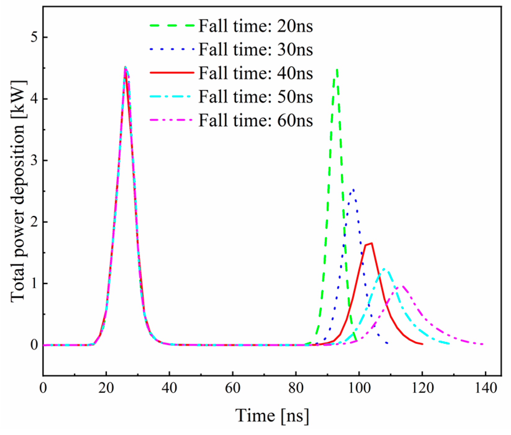
3.2.4. Effect of Fall Time on Discharge Characteristics
The evolution of the NS-SDBD’s discharge current and electron density through time and at various fall times is displayed in Figure 16 and Figure 17. It is obvious that varied fall times have no impact on the discharge current and electron density during the voltage rise, but they do result in a lower peak and a smoother waveform for the second discharge current. This is because a longer fall time gives electrons greater opportunities to collide with gas molecules, thus reducing the second current peak by increasing electron energy loss. Additionally, the longer falling edge duration of the pulse gives the electron recombination more time to occur, which causes the electron density to decrease.
The impact of five various fall times on the total power deposition of NS-SDBD is summarized in Figure 18. It can be observed that a longer rise time leads to a decrease in the total power deposition peak of the second discharge. This is due to the fact that the time and rate of energy release during the discharge process are influenced by the rise time. Longer rise times prolong the duration of the discharge process, resulting in energy release over a longer period of time, which leads to a decrease in current peak and electron density and, consequently, a reduction in total power deposition.
3.3. Discussion
In this study, the discharge behavior of NS-SDBD was investigated through numerical simulations, and key phenomena and parameters during the discharge process were discussed. By studying the voltage amplitude, pulse width, rise time, and fall time of NS-SDBD discharge, the following conclusions were drawn:
- The voltage amplitude has a significant impact on the discharge behavior. Higher voltage amplitudes result in a higher discharge current and electron density. Higher voltage amplitudes generate stronger electric field intensities, facilitating ionization and excitation processes, thereby increasing energy transfer efficiency.
- The pulse width affects the characteristics of the second discharge. A longer pulse width increases the current and electron density of the second discharge, but it has almost no effect on the first discharge. A longer pulse width provides more time for electrons to acquire energy, thereby enhancing the excitation and ionization processes.
- The rise time has an impact on the first discharge but has a smaller effect on the second discharge. A longer rise time leads to a decrease in the peak current and electron density of the first discharge, as well as a delay in the discharge initiation. The results of total power deposition indicate that a longer rise time reduces the energy conversion efficiency of the first discharge but increases the peak value of total power deposition for the second discharge.
- The fall time has an impact on the second discharge but does not affect the discharge characteristics during the voltage-rise process. A longer fall time increases the chance of electron collisions with gas molecules, leading to an increase in electron energy loss. As a result, the peak current and electron density of the second discharge decrease, and the wave form becomes smoother.
In conclusion, the voltage amplitude, pulse width, rise time, and fall time significantly influence the characteristics and total power deposition of NS-SDBD discharges. These findings provide important guidance and theoretical foundations for optimizing the design and application of NS-SDBD. However, there are other factors, such as gas composition and electrode shape, that can also impact NS-SDBD discharges, which can be further explored in future research.
4. Conclusions
Through extensive numerical simulation studies, this study investigated the influence of electrical parameters on the discharge characteristics of the NS-SDBD and achieved the following innovative research findings:
Firstly, by constructing a two-dimensional numerical model based on seven discharge particle chemical reactions, the voltage–current (V-A) characteristics, discharge profile, and spectrum analysis results of the NS-SDBD were extensively investigated. These findings were compared and analyzed with relevant experiments, providing strong support for a deeper understanding of NS-SDBD discharge behavior.
Secondly, a systematic study was conducted on the effects of parameters such as voltage amplitude, pulse width, rise time, and fall time on the discharge characteristics of the NS-SDBD.
By altering the values of these parameters, a number of discharge characteristic curves were obtained for this study, and the variation trend and influence mechanism were examined. The results demonstrate that the NS-SDBD actuator’s discharge current characteristics and spatial distribution performance are significantly influenced by the electrical parameters. The electron ionization process is accelerated by higher voltage amplitudes, causing the discharge current to peak earlier and increase the electron density. A longer pulse width can boost the efficiency of the electron energy transfer and ionization process, prolong the duration that electrons and ions interact, and raise the discharge current. The total power deposition peak for the first discharge declines with longer rise durations, whereas the total power deposition peak for the second discharge rises. A longer fall time affords the electron recombination more time, thus reducing electron density.
The discoveries made in this study hold significant reference value for optimizing the design and performance of NS-SDBD actuators. They are of great importance in driving the development of plasma science and technology and provide new research ideas and directions for researchers in related fields. By fully understanding the influence of electrical parameters on discharge characteristics, it becomes possible to adjust the values of these parameters according to different application scenarios. This enables precise control over the discharge current, electron density, and total power deposition, leading to the optimization of the operational efficiency and performance of NS-SDBD actuators.
Author Contributions
Conceptualization, Y.Y.; methodology, S.L.; software, S.L.; validation, S.L. and Y.Y.; formal analysis, S.L.; investigation, S.L.; resources, Y.Y. and B.Z.; data curation, S.L.; writing—original draft preparation, S.L.; writing—review and editing, Y.Y., B.Z., and Y.M.; visualization, S.L.; supervision, Y.Y.; project administration, Y.Y.; funding acquisition, Y.Y. All authors have read and agreed to the published version of the manuscript.
Funding
This research was supported by the research on high Reynolds number turbulent drag reduction method based on plasma suction pump, Science and Technology Research Project of Chongqing Municipal Education Commission (KJZD-M202100702), a major project.
Institutional Review Board Statement
Not applicable.
Informed Consent Statement
Not applicable.
Data Availability Statement
Not applicable.
Conflicts of Interest
The authors declare no conflict of interest.
References
- Mishra, H.; Bolouki, N.; Hsieh, S.T.; Li, C.; Wu, W.; Hsieh, J.-H. Application of Spectroscopic Analysis for Plasma Polymerization Deposition onto the Inner Surfaces of Silicone Tubes. Coatings 2022, 12, 865. [Google Scholar] [CrossRef]
- Guo, M.; Cui, Y.; Wang, C.; Jiao, J.; Bi, X.; Tao, C. Characterization and Control of Residual Stress in Plasma-Sprayed Silicon Coatings on SiC/SiC Composites. Coatings 2023, 13, 674. [Google Scholar] [CrossRef]
- Sanito, R.C.; You, S.-J.; Wang, Y.-F. Application of plasma technology for treating e-waste: A review. J. Environ. Manag. 2021, 288, 112380. [Google Scholar] [CrossRef] [PubMed]
- Elaissi, S.; Charrada, K. Simulation of Cold Atmospheric Plasma Generated by Floating-Electrode Dielectric Barrier Pulsed Discharge Used for the Cancer Cell Necrosis. Coatings 2021, 11, 1405. [Google Scholar] [CrossRef]
- Zhu, Y.; Wu, Y.; Wei, B.; Xu, H.; Liang, H.; Jia, M.; Song, H.; Li, Y. Nanosecond-pulsed dielectric barrier discharge-based plasma-assisted anti-icing: Modeling and mechanism analysis. J. Phys. D Appl. Phys. 2020, 53, 145205. [Google Scholar] [CrossRef]
- Zhang, X.; Li, H.; Choi, K.S.; Song, L. Coherent structures induced by dielectric barrier discharge plasma actuator. Mod. Phys. Lett. B 2017, 31, 1850038. [Google Scholar] [CrossRef] [Green Version]
- Zhang, C.; Han, L.; Qiu, J.; Shao, T.; Luo, Z.-; Wang, L. A pulsed generator for synchronous discharges of high-energy plasma synthetic jet actuators. IEEE Trans. Dielectr. Electr. Insul. 2017, 24, 2076–2084. [Google Scholar] [CrossRef]
- Benard, N.; Zouzou, N.; Claverie, A.; Sotton, J.; Moreau, E. Optical visualization and electrical characterization of fast-rising pulsed dielectric barrier discharge for airflow control applications. J. Appl. Phys. 2012, 111, 033303. [Google Scholar] [CrossRef]
- Lei, P.; Kun, H.; Qiaogen, Z. The discharge characteristics of surface dielectric barrier discharge sustained by repetitive nanosecond pulses in open air. J. Appl. Phys. 2016, 120, 103302. [Google Scholar] [CrossRef]
- Xie, Q.; Gan, W.; Zhang, C.; Che, X.; Yan, P.; Shao, T. Effect of rise time on nanosecond pulsed surface dielectric barrier discharge actuator. IEEE Trans. Dielectr. Electr. Insul. 2019, 26, 346–352. [Google Scholar] [CrossRef]
- Huang, B.; Zhang, C.; Adamovich, I.V.; Akishev, Y.S.; Shao, T. Surface ionization wave propagation in the nanosecond pulsed surface dielectric barrier discharge: The influence of dielectric material and pulse repetition rate. Plasma Sources Sci. Technol. 2020, 29, 044001. [Google Scholar] [CrossRef]
- Enloe, C.L.; Font, G.I.; McLaughlin, T.E.; Orlov, D.M. Surface Potential and Longitudinal Electric Field Measurements in the Aerodynamic Plasma Actuator. AIAA J. 2008, 46, 2730–2740. [Google Scholar] [CrossRef]
- Singh, K.P.; Roy, S. Modeling plasma actuators with air chemistry for effective flow control. J. Appl. Phys. 2007, 101, 123308. [Google Scholar] [CrossRef] [Green Version]
- Nishida, H.; Nonomura, T.; Abe, T. Numerical Study on Spanwise Nonuniformity in Body-Force Field of Dielectric-Barrier-Discharge Plasma Actuator. AIAA J. 2016, 54, 659–669. [Google Scholar] [CrossRef]
- Wu, Y.; Zhu, Y.; Cui, W.; Jia, M.; Li, Y. Simulation of Nanosecond Pulsed DBD Plasma Actuation with Different Rise Times. Plasma Process. Polym. 2015, 12, 642–654. [Google Scholar] [CrossRef]
- Mertz, B.E.; Corke, T.C. Single-dielectric barrier discharge plasma actuator modelling and validation. J. Fluid Mech. 2011, 669, 557–583. [Google Scholar] [CrossRef]
- Soloviev, V.R.; Krivtsov, V.M. Numerical modelling of nanosecond surface dielectric barrier discharge evolution in atmospheric air. Plasma Sources Sci. Technol. 2018, 27, 114001. [Google Scholar] [CrossRef]
- Ahn, S.; Chae, J.; Kim, H.-J.; Kim, K.H. Numerical Simulation of Streamer Physics in Nanosecond Pulsed Surface Discharges. Int. J. Aeronaut. Space Sci. 2021, 22, 547–559. [Google Scholar] [CrossRef]
- Shi, C.A.; Adamiak, K.; Castle, G.S.P. Numerical study of the characteristics of a dielectric barrier discharge plasma actuator. J. Phys. D Appl. Phys. 2018, 51, 095201. [Google Scholar] [CrossRef]
- Peng, B.; Jiang, N.; Liu, Z.; Yao, X.; Li, J.; Wu, Y. Discharge dynamics of primary and secondary streamers in a repetitively pulsed surface dielectric barrier discharge. J. Appl. Phys. 2022, 131, 113301. [Google Scholar] [CrossRef]
- Xu, S.Y.; Cai, J.S.; Wang, J.F.; Tang, S.J. Characterization of the single nanosecond pulsed surface dielectric barrier plasma actuator: Geometric and electric effects. Contrib. Plasma Phys. 2020, 60, e201900081. [Google Scholar] [CrossRef]
- Unfer, T.; Boeuf, J.P. Modelling of a nanosecond surface discharge actuator. J. Phys. D Appl. Phys. 2009, 42, 194017. [Google Scholar] [CrossRef]
- Abdollahzadeh, M.; Pascoa, J.C.; Oliveira, P.J. Implementation of the classical plasma–fluid model for simulation of dielectric barrier discharge (DBD) actuators in OpenFOAM. Comput. Fluids 2016, 128, 77–90. [Google Scholar] [CrossRef]
- Kossyi, I.A.; Kostinsky, A.Y.; Matveyev, A.A.; Silakov, V.P. Kinetic scheme of the non-equilibrium discharge in nitrogen-oxygen mixtures. Plasma Sources Sci. Technol. 1992, 1, 207–220. [Google Scholar] [CrossRef]
- Alves, L.L. The IST-LISBON database on LXCat. J. Phys. Conf. Ser. 2014, 565, 012007. [Google Scholar] [CrossRef]
- Hagelaar, G.J.M.; Pitchford, L.C. Solving the Boltzmann equation to obtain electron transport coefficients and rate coefficients for fluid models. Plasma Sources Sci. Technol. 2005, 14, 722–733. [Google Scholar] [CrossRef]
- Leonov, S.B.; Adamovich, I.V.; Soloviev, V.R. Dynamics of near-surface electric discharges and mechanisms of their interaction with the airflow. Plasma Sources Sci. Technol. 2016, 25, 063001. [Google Scholar] [CrossRef]
- Peng, B.; Jiang, N.; Yao, X.; Ruan, Y.; Wang, D.; Shang, K.; Lu, N.; Namihira, T.; Li, J.; Wu, Y. Experimental and numerical studies of primary and secondary streamers in a pulsed surface dielectric barrier discharge. J. Phys. D Appl. Phys. 2019, 52, 325202. [Google Scholar] [CrossRef]
- Shao, T.; Jiang, H.; Zhang, C.; Yan, P.; Lomaev, M.I.; Tarasenko, V.F. Time behaviour of discharge current in case of nanosecond-pulse surface dielectric barrier discharge. Europhys. Lett. 2013, 101, 45002. [Google Scholar] [CrossRef]
- Paris, P.; Aints, M.; Valk, F.; Plank, T.; Haljaste, A.; Kozlov, K.V.; Wagner, H.-E. Intensity ratio of spectral bands of nitrogen as a measure of electric field strength in plasmas. J. Phys. D Appl. Phys. 2005, 38, 3894–3899. [Google Scholar] [CrossRef] [Green Version]
- Yun, W.; Yinghong, L.; Min, J.; Huimin, S.; Changbing, S.; Yikang, P. Experimental Investigation into Characteristics of Plasma Aerodynamic Actuation Generated by Dielectric Barrier Discharge. Chin. J. Aeronaut. 2010, 23, 39–45. [Google Scholar] [CrossRef] [Green Version]
Figure 1.
Schematic of the NS-SDBD actuator configuration.

Figure 2.
Computational domain of simulation.
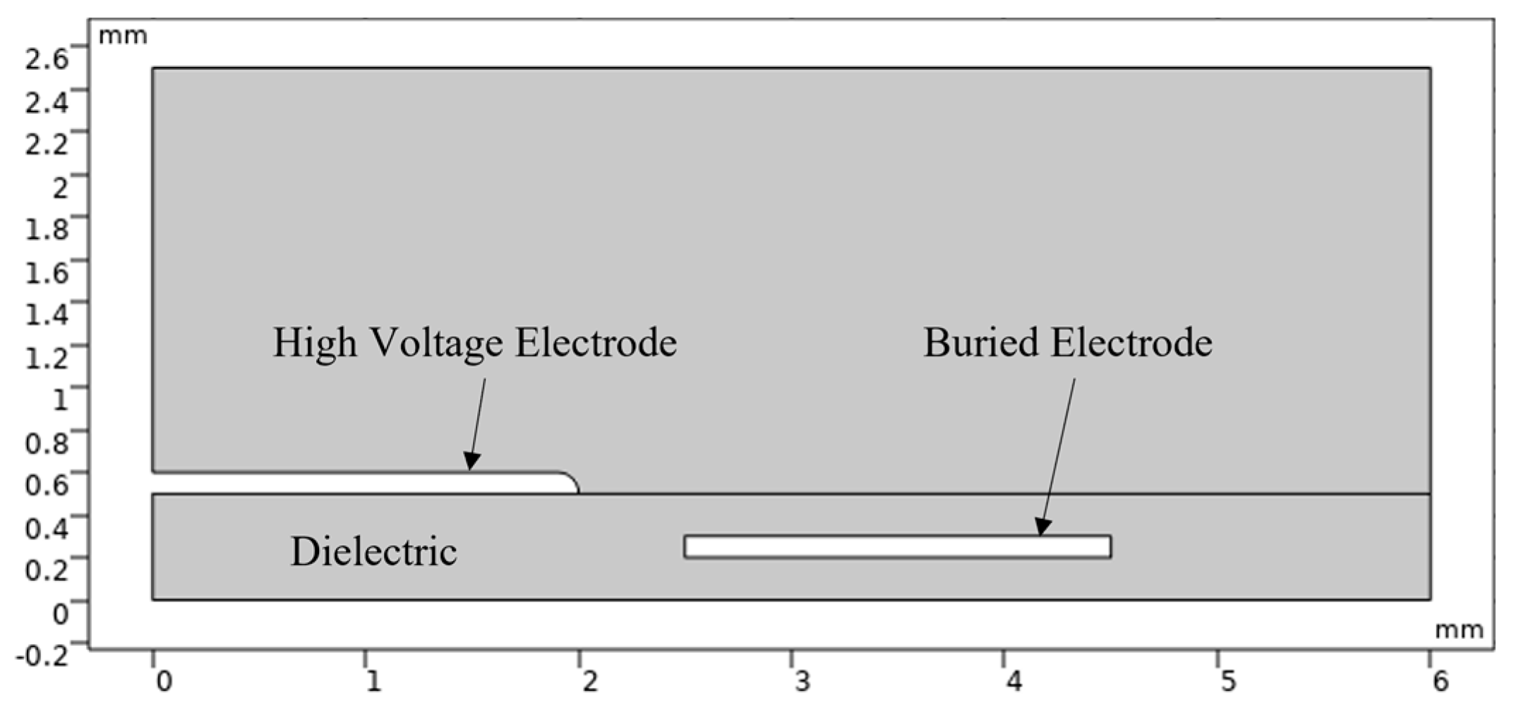
Figure 3.
Calculated V-A characteristics.

Figure 4.
Distribution of electrons in logarithm.
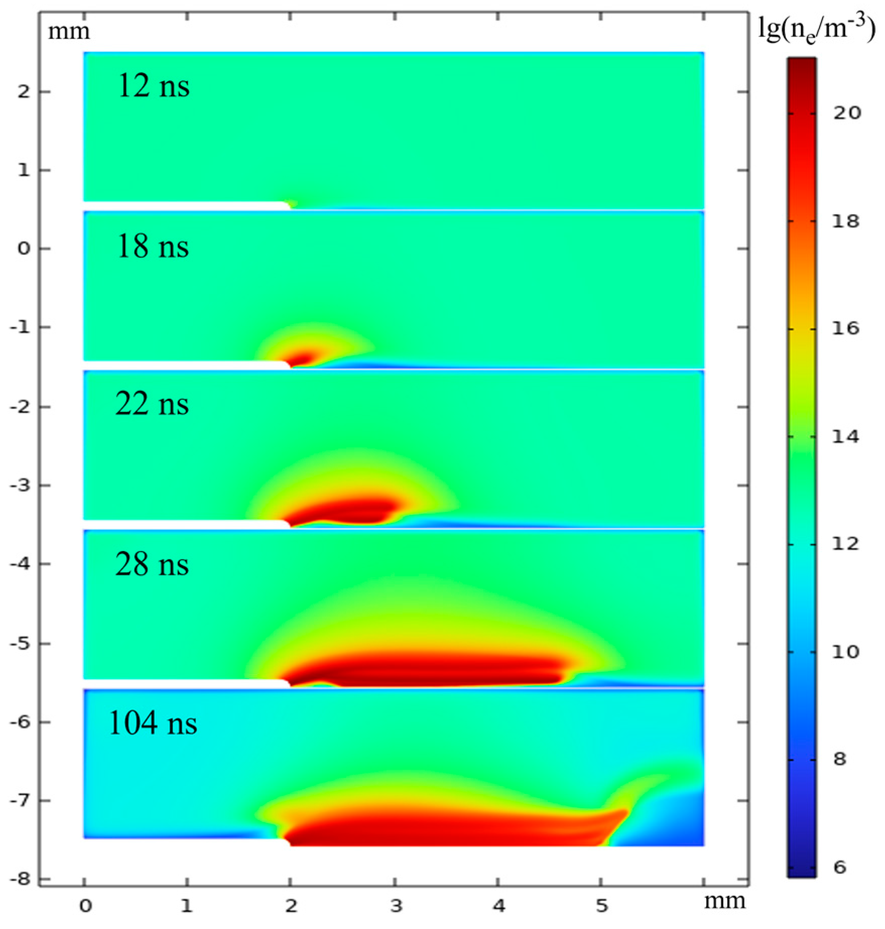
Figure 5.
Distribution of electric field strength.

Figure 6.
Calculated and time-averaged result.
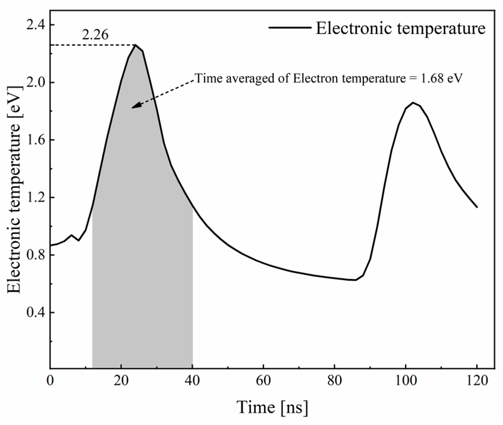
Figure 7.
The current characteristics of NS-SDBD under various voltage amplitudes.

Figure 8.
Effects of various voltage amplitudes on electron density.
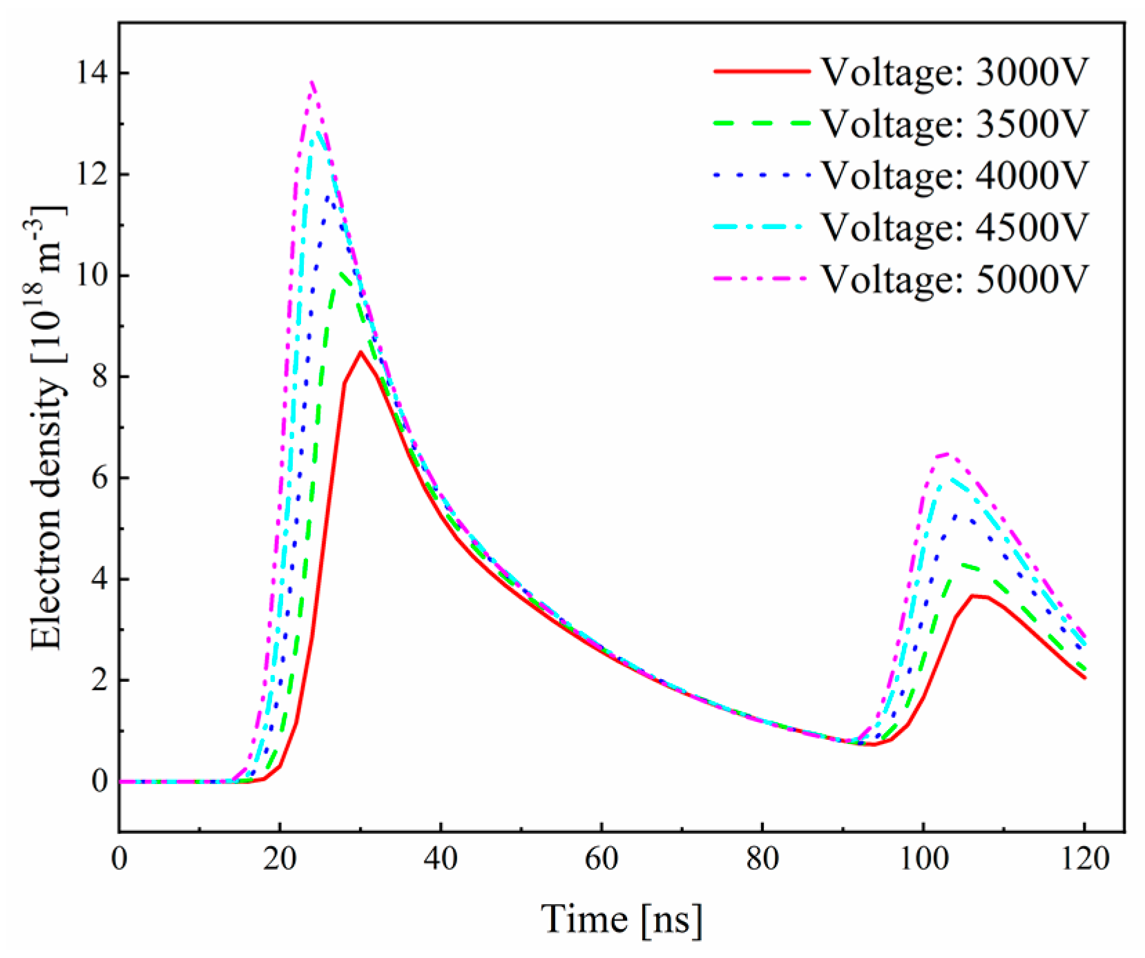
Figure 9.
Effects of various voltage amplitudes on total power deposition.
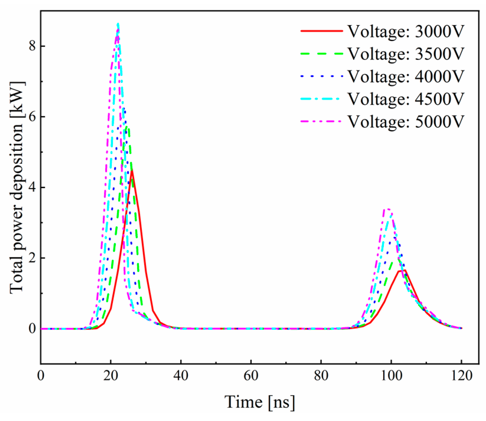
Figure 10.
The current characteristics of NS-SDBD under various pulse widths.
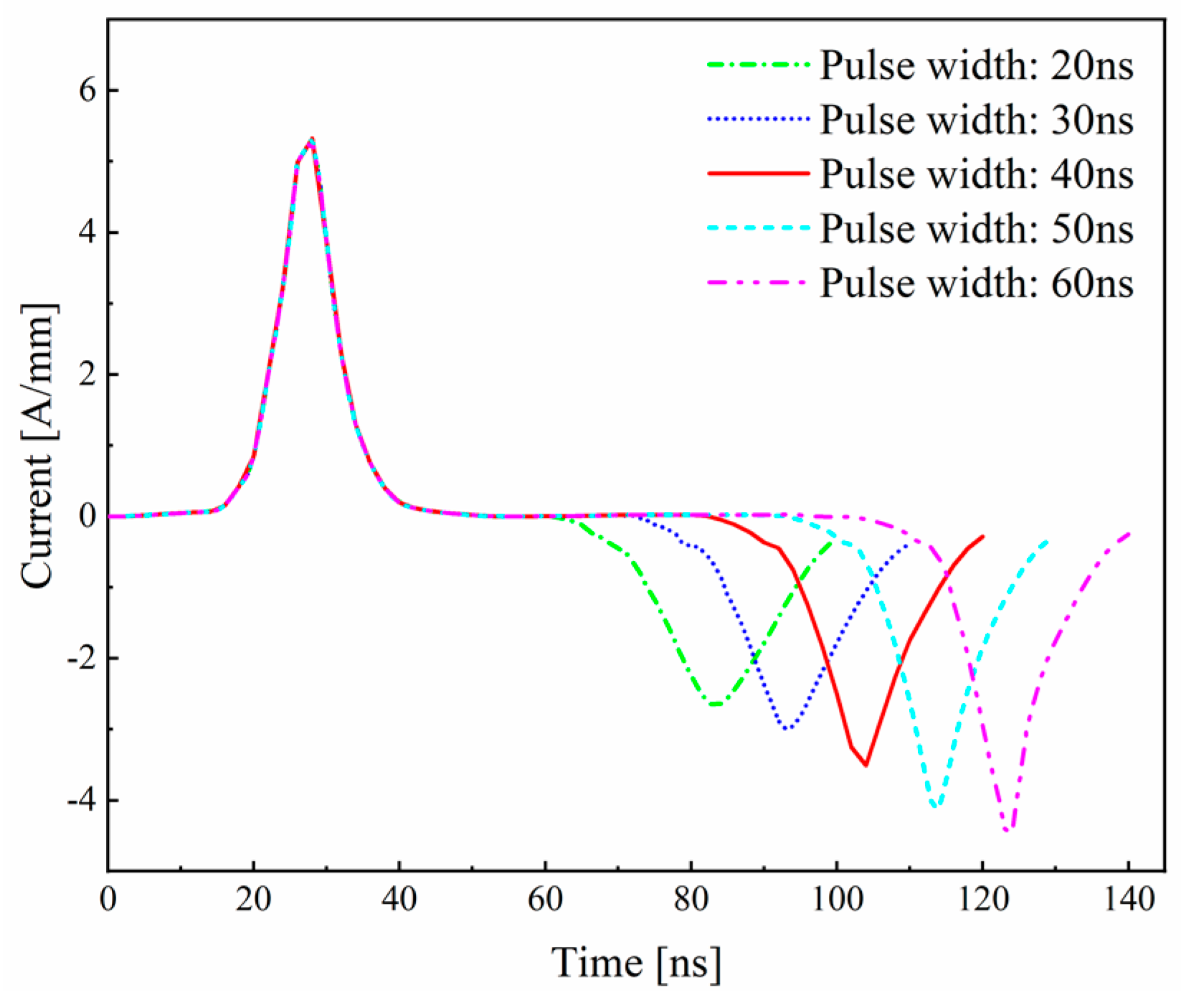
Figure 11.
Effects of various pulse widths on electron density.

Figure 12.
Effects of various pulse widths on total power deposition.
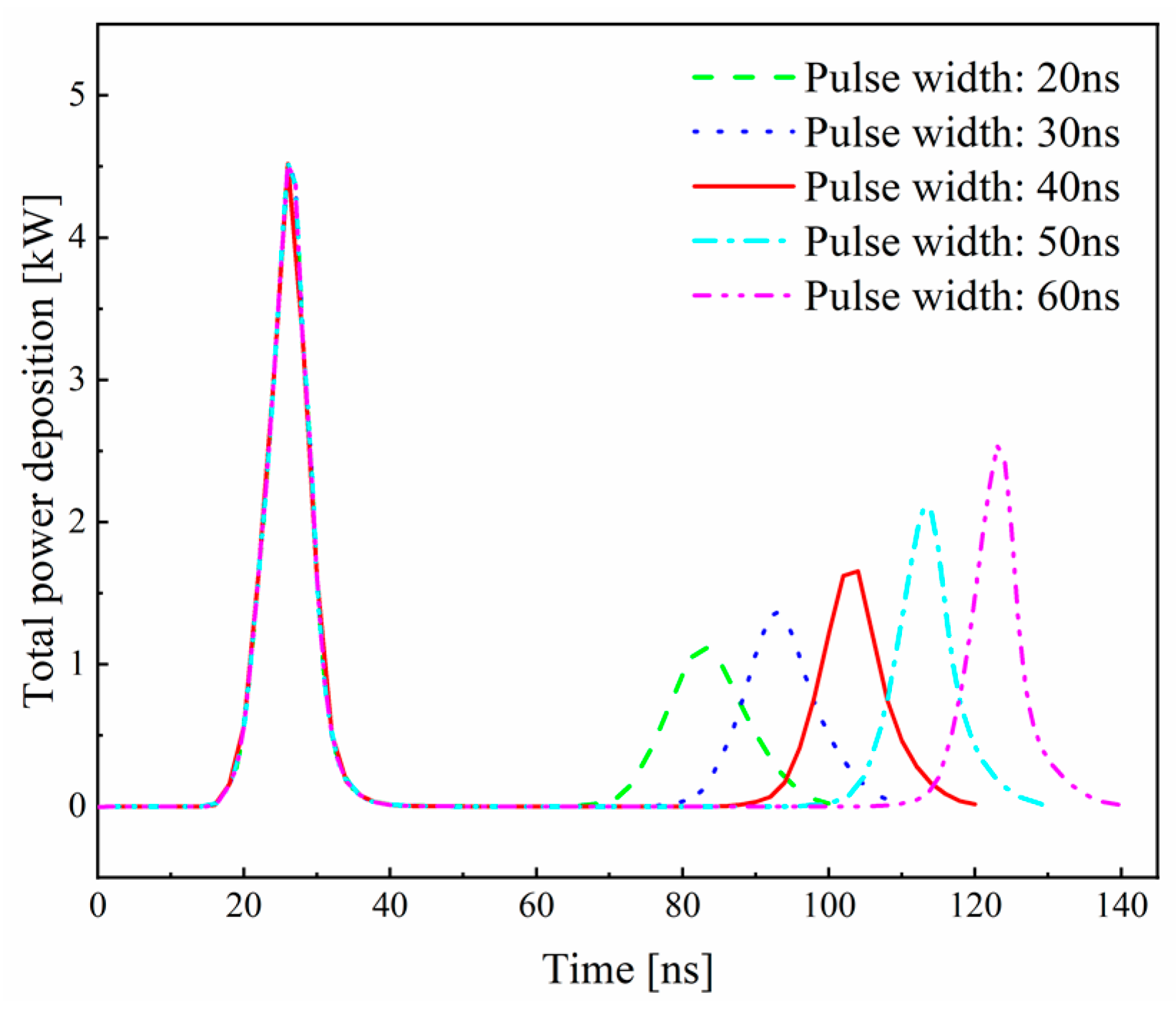
Figure 13.
The current characteristics of NS-SDBD under various rise times.

Figure 14.
Effects of various rise times on electron density.

Figure 15.
Effects of various rise times on total power deposition.
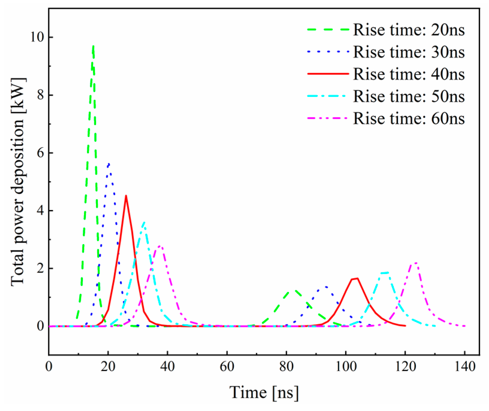
Figure 16.
The current characteristics of NS-SDBD under various fall times.
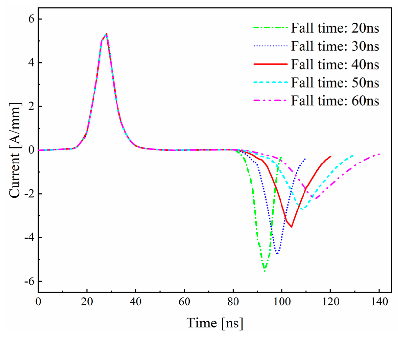
Figure 17.
Effects of various fall times on electron density.

Figure 18.
Effects of various fall times on total power deposition.

Table 1.
Reactions and the rate coefficients.
| Sequence | Reaction Equations | Rate Coefficient |
|---|---|---|
| R 1 | e + N2 => e + N2 | α1 |
| R 2 | e + O2 => e + O2 | α2 |
| R 3 | e + 2O2 => O2 + O2− | α3 |
| R 4 | e + O2 => O2+ + 2e | α4 |
| R 5 | e + N2 => N2+ + 2e | α5 |
| R 6 | e + O2 => O2− | α6 |
| R 7 | e + N2+ => N2 | 4.65 × 10¹⁰ × (Te)−0.5 |
| R 8 | e + N2+ => N2 | 2.4 × 10⁶ |
| R 9 | O2+ + O2− => 2O2 | 1.2 × 10¹¹ |
| R 10 | 2e + N2+ => N2 + e | 2.6 × 10⁹ × (Te)−4.5 |
| R 11 | 2e + O2+ => O2 + e | 2.6 × 10⁹ × (Te)−4.5 |
| R 12 | O2+ + O2− + O2 => 3O2 | 7.25 × 10¹⁰ |
| R 13 | O2+ + O2− + N2 => 2O2 + N2 | 7.25 × 10¹⁰ |
Table 2.
Surface reactions and the sticking coefficients.
| Sequence | Reaction Equations | Sticking Coefficient |
|---|---|---|
| R 1 | N2+ => N2 | 1 |
| R 2 | O2+ => O2 | 1 |
| R 3 | O2− => O2 | 1 |
| R 4 | O => 0.5O2 | 1 |
| R 5 | O+ => 0.5O2 | 1 |
| R 6 | O− => 0.5O2 | 1 |
Disclaimer/Publisher’s Note: The statements, opinions and data contained in all publications are solely those of the individual author(s) and contributor(s) and not of MDPI and/or the editor(s). MDPI and/or the editor(s) disclaim responsibility for any injury to people or property resulting from any ideas, methods, instructions or products referred to in the content. |
© 2023 by the authors. Licensee MDPI, Basel, Switzerland. This article is an open access article distributed under the terms and conditions of the Creative Commons Attribution (CC BY) license (https://creativecommons.org/licenses/by/4.0/).
Share and Cite
MDPI and ACS Style
Liang, S.; Yu, Y.; Zheng, B.; Mao, Y. Numerical Investigation on the Effect of Electrical Parameters on the Discharge Characteristics of NS-SDBD. Coatings 2023, 13, 1237. https://doi.org/10.3390/coatings13071237
AMA Style
Liang S, Yu Y, Zheng B, Mao Y. Numerical Investigation on the Effect of Electrical Parameters on the Discharge Characteristics of NS-SDBD. Coatings. 2023; 13(7):1237. https://doi.org/10.3390/coatings13071237
Chicago/Turabian StyleLiang, Sijia, Yang Yu, Borui Zheng, and Yuepeng Mao. 2023. "Numerical Investigation on the Effect of Electrical Parameters on the Discharge Characteristics of NS-SDBD" Coatings 13, no. 7: 1237. https://doi.org/10.3390/coatings13071237
Note that from the first issue of 2016, this journal uses article numbers instead of page numbers. See further details here.