Article

Active Broadband Absorber Based on Phase-Change Materials Optimized via Evolutionary Algorithm

1
School of Physics and Optoelectronic Engineering, Yangtze University, Jingzhou 434023, China
2
School of Computing, Queen’s University, Kingston, ON K7L 2N8, Canada
3
School of Microelectronics and Control Engineering, Changzhou University, Changzhou 213164, China
4
College of Electronic and Optical Engineering, Nanjing University of Posts and Telecommunications, Nanjing 210023, China
5
College of Physics and Electronics, Central South University, Changsha 410083, China
6
Research Center for Photonic Technology, Fujian Key Laboratory for Advanced Micronano Photonics Technology and Devices & Key Laboratory of Information Functional Material for Fujian Higher Education, Quanzhou Normal University, Quanzhou 362000, China
7
Joint Laboratory for Extreme Conditions Matter Properties, Tianfu Institute of Research and Innovation, State Key Laboratory of Environmental Friendly Energy Materials, Key Laboratory of Manufacturing Process Testing Technology of Ministry of Education, Southwest University of Science and Technology, Mianyang 621010, China
8
Guangxi Key Laboratory of Precision Navigation Technology and Application, Guilin University of Electronic Technology, Guilin 541004, China
*
Authors to whom correspondence should be addressed.
Coatings 2023, 13(9), 1604; https://doi.org/10.3390/coatings13091604
Submission received: 10 August 2023 / Revised: 7 September 2023 / Accepted: 13 September 2023 / Published: 14 September 2023
(This article belongs to the Special Issue Micro-Nano Optics and Its Applications)

Abstract

:
This article proposes a temperature-controlled absorber based on VO2, which consists of five layers: a disk-shaped VO2 layer array, a dielectric layer, a circular hole VO2 array, a SiO2 layer, and a gold substrate from top to bottom. We optimized the thickness of the other four layers of the absorber, except for the gold layer, using PSO. After ten iterations, we determined that the optimal parameters for the top-to-bottom four-layer thicknesses were 0.183 μm, 0.452 μm, 0.557 μm and 1.994 μm. At this point, our absorber reached the optimal absorption parameters, and we plotted the absorption spectrum under these conditions. We found that the absorption rate at 29.1–47.2 THz was higher than 90%, and the absorption bandwidth was as high as 18.1 THZ. This frequency band covers most of the atmospheric window area (23–37.5 THz), so it will have good practicality. At 30.8 THz and 43.12 THz, there were perfect absorption peaks with absorption rates of 99.99% and 99.99%, respectively. We explained the cause of absorption from the perspective of electric field, and then we studied the change in the absorption curve of the absorber when the temperature of VO2 changed, and we can directly observe the changes in the electric field to explain this. Finally, we can tune the bandwidth and absorption rate of the absorber by changing the structure of the VO2 pattern. After comparing with other absorbers developed in recent years, our absorber still has good competitiveness, and we believe that our solution is expected to have outstanding performance in fields such as photothermal conversion and thermal stealth in the future.

1. Introduction

A metamaterial is a synthetic material, which means it is not naturally occurring. Because of metamaterial’s customizable electromagnetic properties, it can readily exhibit electromagnetic characteristics that natural materials lack, thus greatly expanding the potential applications of metamaterials [1,2,3,4,5,6]. In the field of absorbers, the research of Landy’s team in 2008 led to the upsurge of applying metamaterials to absorbers [7]. Since then, metamaterial absorbers have been widely used in thermal radiation absorption, optical stealth, intelligent windows and other fields [8,9,10,11,12], while metamaterial narrowband absorbers have outstanding performance in sensor, detection and other fields [13,14,15,16,17].
At present, metamaterials such as Dirac metal, Graphene, and VO2 are most widely used in metamaterial absorbers [18,19,20,21,22]. This is due to the phase-change characteristics of VO2 discovered by Bell Labs in 1959 [23], namely that VO2 is in an insulating state at room temperature, and when it is heated to 340 K, it transitions into a metallic state. Because the phase-change temperature is closer to room temperature than other materials, researchers have always been enthusiastic about VO2 research. In 2021, Zhong [24] proposed an absorber based on a combination of gold and VO2 layers. The pattern of the absorber is composed of a cross-shaped array, with a broadband absorption rate of over 90% at 17–26 THz. In 2023, Kwang’s [25] team proposed an absorber based on a toroidal VO2 array. The absorber has three broadband absorption peaks with an absorption bandwidth of more than 2.42 THz and an absorption rate of more than 90% in the terahertz band. So far, the proposed broadband absorber based on VO2 has an absorption rate of more than 90%, and the absorption bandwidth is mostly within 10 THz, rarely more than 10 THz. The development direction of broadband absorber must aim for a broader absorption bandwidth while maintaining high absorption rates, which is the direction that researchers need to focus on.
Particle swarm optimization (PSO) is a randomized algorithm proposed by James and Russell in 1995. Inspired by the foraging behavior of birds, PSO initializes the algorithm to randomly assign each particle in the search space, and at the same time, it gives each particle an adaptive speed. Particles can remember the best position they have ever been to, and particle are influenced by three factors: the best position it has ever been to, the best global position, and the initial velocity, resulting in a composite acceleration that iterates to the optimal solution [26]. Compared with other optimization algorithms, PSO has the advantages of wide application range, high computing efficiency, and adaptive adjustment of search strategies.
In this article, we propose a double-layer VO2 absorber based on a circular hole and disk array, and we optimize its parameters with an improved PSO. The results show that in the frequency range of 29.1–47.2 THz, the absorption rate is above 90%, and the total absorption bandwidth is as high as 18.1 THz. When VO2 transitions from an insulating state to a metallic state, the highest absorption rate of the absorber increases from 10.3% to 99.99%. We explained the reason for this transition from the perspective of an electric field. Furthermore, we discussed the impact of changing structural parameters on the absorber and addressed the effect of changing the incident angle on the absorber toward the end of the article. Our absorbers have good application prospects in fields such as solar energy absorption and stealth coatings.

2. Particle Swarm Optimization

Earlier, we mentioned the basic concept of PSO. We know that the most important thing in PSO is to iterate the position and speed of particles as well as the optimization strategy [27,28]. Although the traditional PSO is convenient to search the optimal solution globally, it takes a long time to search locally, so we chose the improved particle swarm optimization algorithm. The iteration formula of speed and position is as follows [29,30]:
n e w v = w v + c 1 r a n d g b e s t x + c 2 r a n d p b e s t x
n e w x = x + n e w v
w = w m a x d m a x d w m i n
where w is the inertia weight, v and x are the current velocity and position, n e w v and n e w x are the updated velocity and position, c 1 and c 2 are acceleration constants, r a n d is a random number within 1, and g b e s t and p b e s t are global and local optimal parameters, respectively. We have defined the weight w that varies with the number of iterations, as shown in Formula (3). We define w m a x as 0.9 and w m i n as 0.4. This way, as the iteration progresses, the algorithm switches from searching for global optimal values to searching for local optimal values, greatly enhancing the accuracy and efficiency of the search [31].
In the combination of absorbers and the PSOs in the past, most researchers often choose the average absorption rate of the region as the figure of merit (FOM), which ignores the need for broadband absorbers to meet a wider absorption bandwidth. Therefore, after discussion, we define the formula of FOM as follows [32,33,34]:
F O M =   b w p r e / b w t o t a l
where b w p r e is the absorption bandwidth with an absorption rate higher than 90%, and b w t o t a l is the total bandwidth selected.
Unfortunately, due to the inherent nature of the algorithm, PSO algorithm cannot be well applied in the current hot field of hypersurface inverse design, like random forest (RF) and deep learning (DP). However, in terms of optimization problems, PSO has rare advantages compared to the above two algorithms.

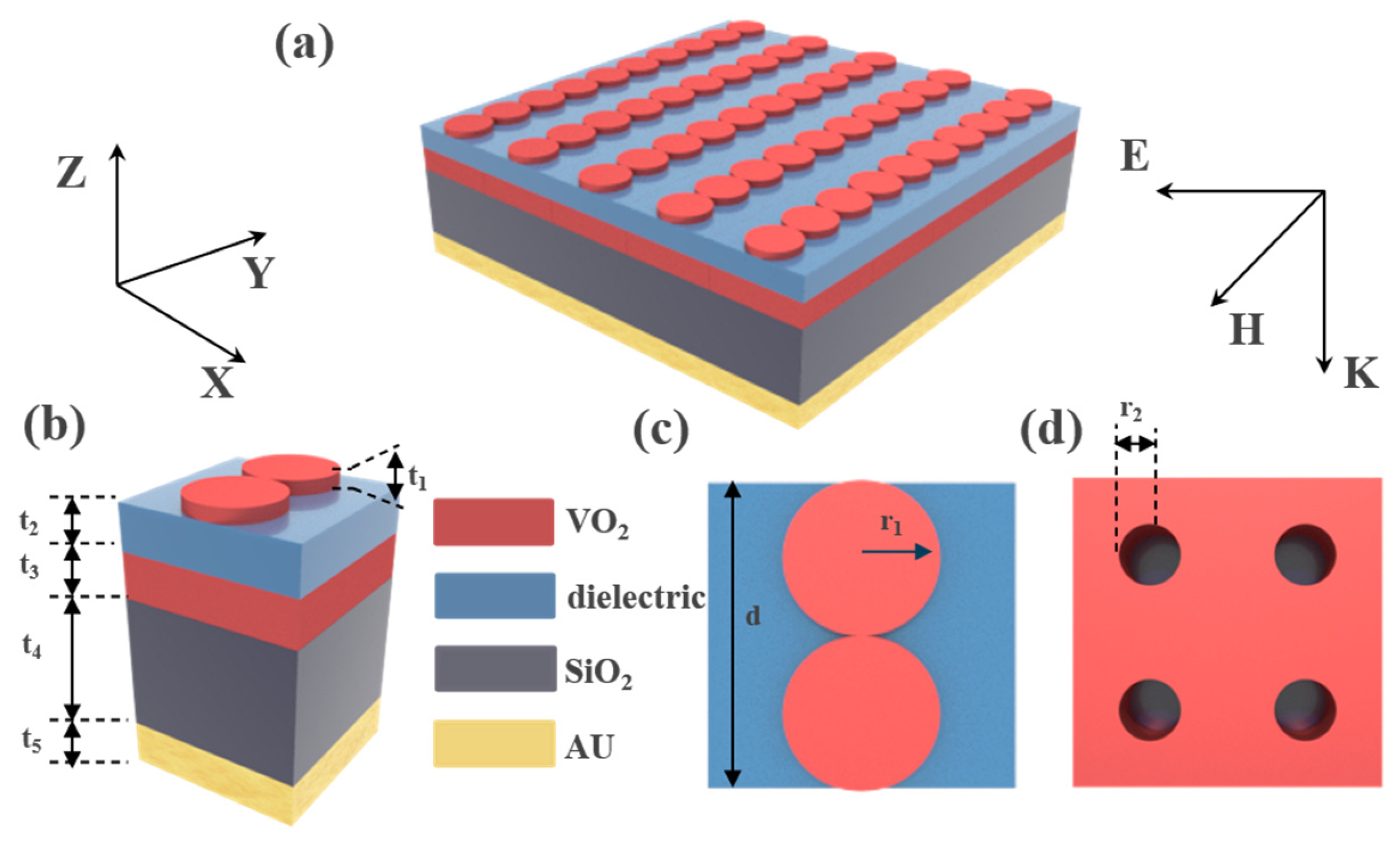
3. Design and Method

As shown in Figure 1a, the absorber we designed has a five-layer structure, consisting of a disk VO2 array, a Topas layer, a circular hole VO2 array, a SiO2 layer, and a gold layer from top to bottom. Among them, the radius of circular VO2 is r1 = 0.5 μm, the thickness t1 = 0.183μm, the refractive index of dielectric layer is 2.35 [35,36], the thickness t2 = 0.452 μm, the radius of circular hole VO2 is r2 = 0.29 μm, the thickness t3 = 0.557 μm, the refractive index of SiO2 layer is 1.90, the thickness t4 = 1.994 μm, and the dielectric constant of the bottom gold layer is described using the drude model, where the plasma frequency ω p = 1.37 × 10 16   s 1 , and the damping constant γ = 1.23 × 10 14   s 1 , with a thickness t5 = 0.2 μm [37,38]. Due to the difficulty in making the absorber we proposed, we have proposed the following production method: first, we deposit a layer of gold on a silicon wafer as the base, and then we prepare a SiO2 layer on the gold through chemical vapor deposition. Then, VO2 thin films are generated through magnetron sputtering, and circular holes are generated through chemical etching. For the top layer of VO2 disk, due to its small thickness, ion beam etching can be used to generate it.
The dielectric constant of VO2 can be described by the following drude model [39,40]:
ε ω = ε ω p 2 ω ( ω + i γ )
where ε = 12 , damping frequency γ = 5.75 × 10 13   rad / s , plasma frequency ω p ( σ ) = ω p ( σ 0 ) σ / σ 0 , where ω p ( σ 0 ) = 1.4 × 10 15   rad / s   σ 0 = 3 × 10 5   S / m , and without specific instructions, we use the conductivity σ = 2 × 10 6   S / m of VO2 at a temperature of 345 K. We use FDTD Commercial software (Lumerical_2020 R2) for simulation, and the input light wave is the TE wave perpendicular to the absorber surface [41,42]. (See Table 1).
The iterative operation of FOM is shown in Figure 2b. When the iteration reaches the tenth time, the optimal solution is obtained. Compared with DP, which requires thousands of training sets and genetic algorithms that require at least fifteen iterations [43], PSO has better speed to achieve the optimal value. The optimal values of the four parameters we obtain are t1 = 0.183 μm, t2 = 0.452 μm, t3 = 0.557 μm, and t4 = 1.994 μm, respectively. At this point, our absorber reaches its maximum bandwidth above 90%:

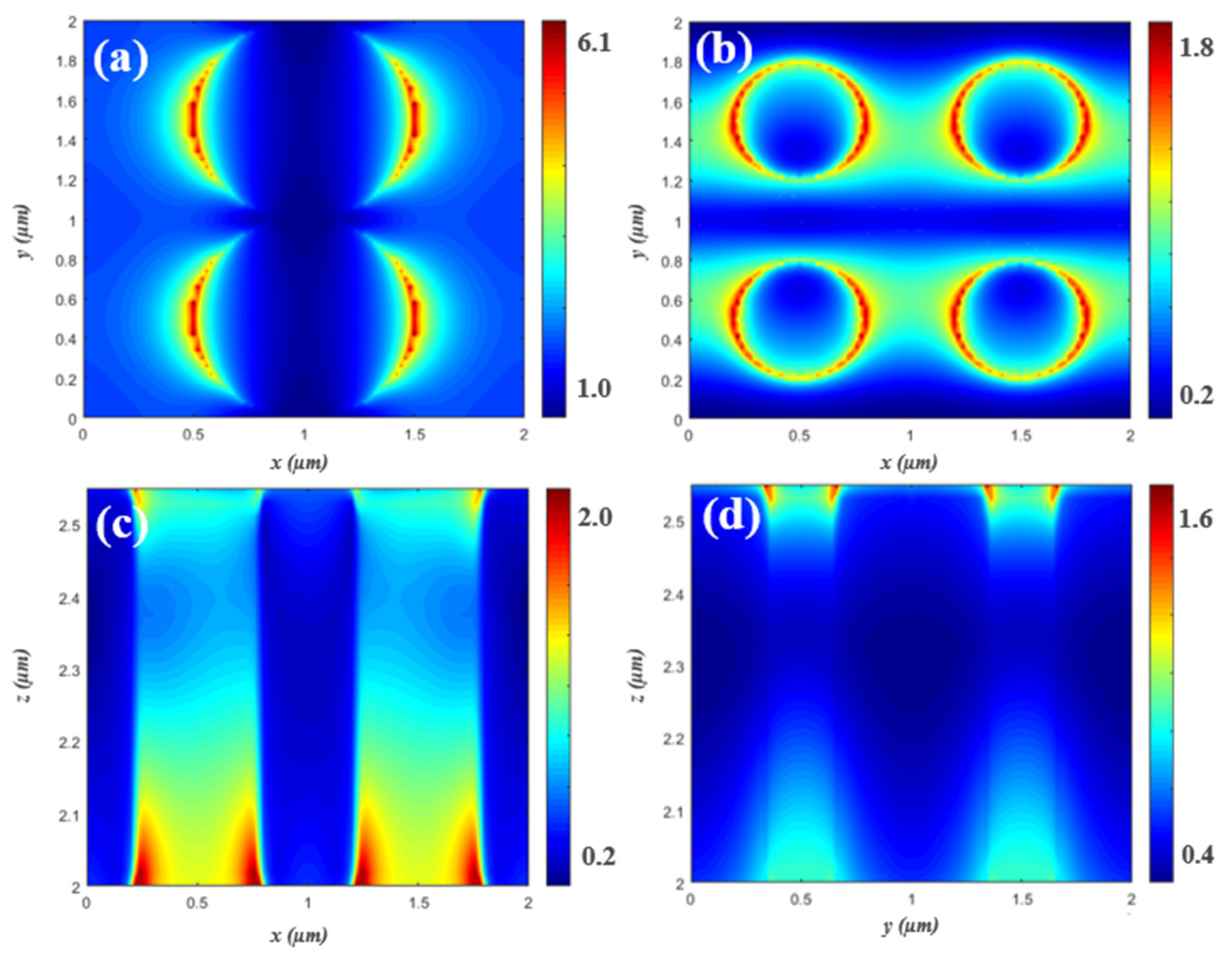
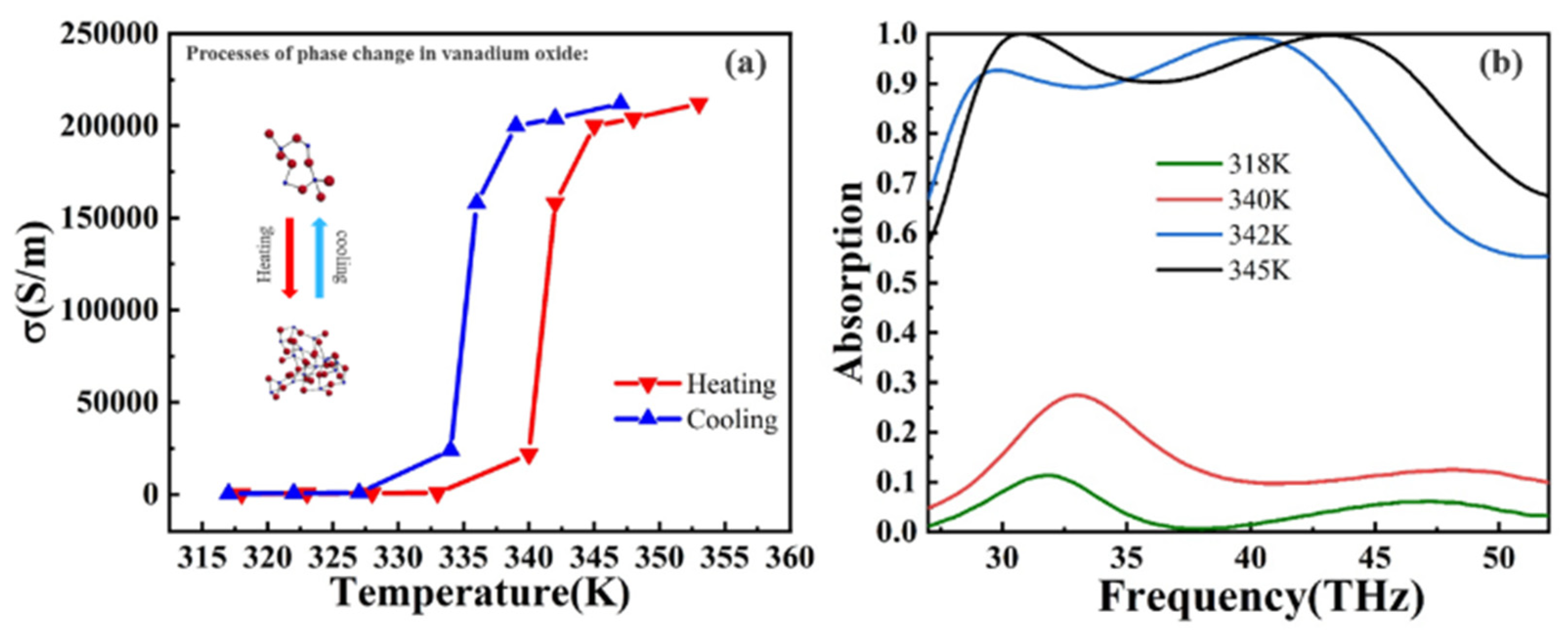
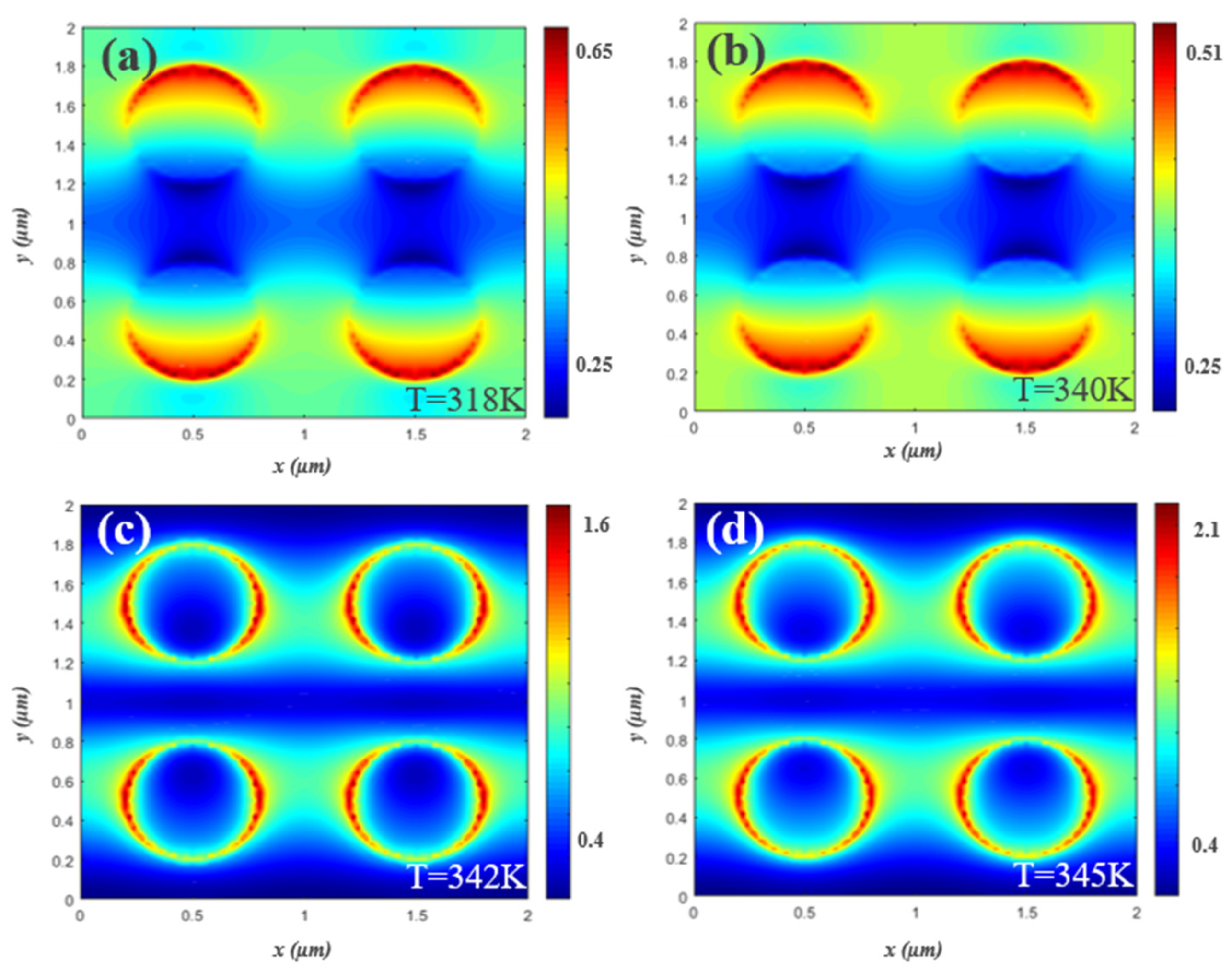
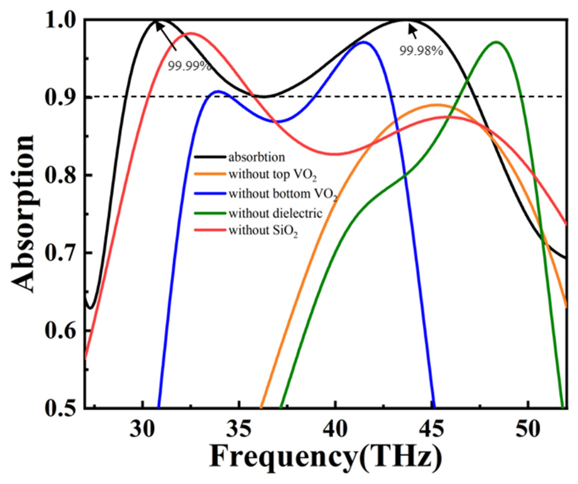
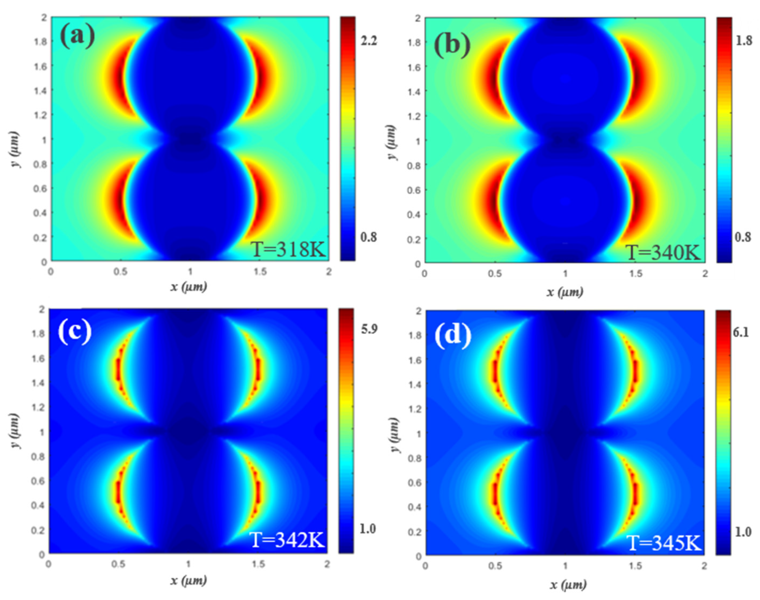
4. Results and Discussions

Figure 3 shows the absorption spectrum of our absorber. The black curve in the figure shows the absorption curve when both the upper and lower layers of VO2 are present, the orange curve shows the absorption curve when removing the top VO2, the blue curve shows the absorption curve when removing the bottom VO2 layer, the green curve shows the absorption curve when removing the upper dielectric layer, and the red curve shows the absorption curve when removing the SiO2 layer. At this point, we can clearly see that when we remove any layer structure, the absorption rate can reach up to 97.23%, and the absorption bandwidth above 90% can only reach up to 6.73 terahertz. However, when the five-layer structure is present, the absorption rate can reach up to 99.99%. The absorption bandwidth above 90% is 29.1–47.2 THz, with a maximum of 18.3 THz. The absorption rates at frequencies of 30.74 THz and 43.36 THz reach 99.99% and 99.98%, respectively, achieving perfect absorption. At this time, our absorber has good bandwidth and absorption rate. At the same time, the range of 23–37.5 THz is the atmospheric window, which has a high overlap with our absorption frequency band, which expands the application range of our absorber.
In order to explore the reason for the change of absorption rate and absorption bandwidth, we give an explanation from the perspective of electric field.
Figure 4a and Figure 5a show the absorption spectra in the XY direction when both the double layer VO2 layer and only the top VO2 layer exist. From these two figures, we can intuitively see that when the bottom VO2 layer is removed, the intensity of the electric field in the upper layer VO2 decreases. At the same time, the electric field attached to the x direction of the disk undergoes some dissipation, flowing towards the surrounding medium, resulting in a decrease in absorption [44,45]. Figure 4b–d and Figure 5b–d shows the absorption spectra of the bottom VO2 layer in the XY, XZ, and YZ directions. Figure 4b–d show the absorption spectra when the top VO2 layer exists, and Figure 5b–d show the absorption spectra when the top VO2 layer is removed. From Figure 5b–d, we can see that when there is only the bottom VO2 layer, the electric field undergoes large-scale resonance in the cavity inside the circular hole and the upper layer of the ring. Local surface plasmon resonance occurs at the bottom of the circular hole, and the intensity of the electric field is also low [46,47]. From Figure 4b–d in comparison, we can see from the electric field graph in the XY direction that the large-scale resonance inside the circular hole has disappeared. By observing the electric field patterns in the XZ and YZ directions, we found that surface plasmon resonance appeared in the upper layer of the circular hole, and the overall electric field intensity also increased significantly, enhancing the absorption of light [48,49]. In summary, the presence of double-layer VO2 enhances the local surface plasmon resonance of VO2, reduces large-scale resonance, and increases the absorption of light via the absorber, which explains why we use double-layer VO2.
The specific crystal structure of VO2 results in its phase transition [50,51]. As shown in Figure 6a, we have plotted the effect of VO2 at different temperatures on the absorption curve of the absorber under heating, At the same time, we can see the phenomenon of conductivity hysteresis during the heating and cooling processes, which is usually considered to be caused by the combined effect of thermal expansion coefficient and internal stress [52,53]. We found that when VO2 is at 318 K, which is maintained at a low temperature, the overall absorption rate of the absorber is within 12%. However, when the temperature is heated to 340 K, VO2 begins to phase change, and the overall absorption rate of the absorber increases, with the highest absorption rate reaching 28.7%. As the temperature further increases, we can see that the absorption bandwidth and overall absorption rate of the absorber are also increasing. At 342 K, the absorption bandwidth with an absorption rate of more than 90% reaches 14 THz, and at 345 K, when the maximum absorption at both ends reaches perfect absorption, the absorption rate is higher than 90%, and the absorption band width reaches 16.9 THz. In conclusion, we can adjust the temperature to make the VO2 phase change, so as to tune the absorption rate and absorption bandwidth of the absorber, which makes our absorber more flexible in practical applications.
Similarly, we also studied the electric field diagrams of absorbers under different temperature conditions. As shown in Figure 7 and Figure 8, we have plotted the electric field diagrams of the top and bottom VO2 layers of the absorber when VO2 is heated from 318 K to 345 K. We find that when the temperature rises, VO2 changes from an insulating state to a metallic state, and the electric field intensity of the absorber increases. At the same time, local surface plasmon resonance occurs around the top disc-shaped VO2 and the bottom circular hole VO2 inner cavity, which enhances the absorption of light [54,55,56]. The electric field diagrams in Figure 7 and Figure 8 also prove this.
In order to expand the application field of our absorber, we also conducted research on the structure of the circular hole in VO2 thin film and VO2 circular disk. We first studied the radius of the circular hole. With the change in the radius, the absorption curve of the absorber has changed, as shown in Figure 9a. When the circular hole radius is 0.23 μm, the maximum absorption rate of the two peaks from left to right is 30.24 THz and 44.03 THz, respectively, 99.95% and 99.64%. The minimum absorption rate between the two peaks is 88.24%. At this time, the absorption rate at 29.13–35.04 THz and 39.08–47.51 THz is higher than 90%, and the absorption bandwidth is 14.33 THz; When the radius of the circular hole gradually increases to 0.35 μm, the maximum absorptivity of the two peaks from left to right is 30.31 THz and 42.53 THz, 99.99% and 99.53%, respectively, and the minimum absorptivity between the two peaks is 93.04%. At this time, the absorptivity at 29.02–46.24 THz is higher than 90%, and the absorption bandwidth is 17.12 THz. In conclusion, when we adjust the radius of the circular hole from 0.23 μm to 0.35 μm, there is no significant impact on the absorptivity of the two absorption peaks of the absorber, But the absorption peak on the right has undergone a red shift, and the lowest absorption rate between the two peaks has increased [57,58]. Therefore, we can control the frequency of the absorption peak on the right and the lowest absorption rate of broadband absorption by adjusting the radius of the ring.
Next, we will explore the effect of changing the radius of the disk on the absorber. Figure 9b shows the absorption spectrum when we adjusted the disk radius from 0.6 μm to 0.4 μm. We can intuitively see that as the radius decreases, the left peak of the absorber shifts from 26.12 THz blue to 34.63 THz, the absorption rate increased from 97.54% to 99.99% and then decreased to 98.12%, and the absorption rate of the right peak increases from 98.63% to 99.12%. However, the minimum absorption rate between the two peaks increases from 75.36% to 97.21%, and at a radius of 0.4 μm, the absorption rates at 34.11–44.36 THz are all greater than 97%; that is, the perfect absorption with an absorption bandwidth of 10.25 THz is achieved.
In order to study the practical value and advantages of our absorber, we also discussed the situation at different incidence angles [59,60]. The scanned images of TE and TM waves are shown in Figure 10 and are compared with other absorbers developed in recent years, as shown in Table 2 [61,62,63,64,65]. Figure 10a shows the scanning pattern of TE waves with changes in incident angle. We can see that the absorption curve of the TE wave with an absorption bandwidth of 30–47 THz at an incidence angle of 0–50° has always kept the absorptivity above 80%, and the absorptivity of the two absorption peaks has always been kept above 90%; since our absorber is asymmetric, the TM wave is slightly different from the TE wave, as shown in Figure 10b. When the incident angle is 0–50°, the absorption curve of TM wave is kept above 80% at the absorption bandwidth of 32–49 THz and above 90% at 41–45 THz. In summary, our absorber can still maintain a high absorption rate of over 80% when the incident angle is 0–50°, so it has good practical value [66,67].

5. Conclusions

This article proposes a temperature-tunable absorber based on VO2, which consists of a VO2 layer, dielectric layer, VO2 layer, SiO2 layer, and gold substrate from top to bottom. The top VO2 layer is an array composed of double-disk patterns, and the bottom VO2 layer is an array composed of four circular patterns, all of which are simple patterns and easy to process. We applied the PSO algorithm to determine the structure of our absorber and provided an optimization strategy suitable for our absorber, determining the optimal value within ten iterations. We drew the absorption spectrum of the absorber and found that the absorption bandwidth of 29.1–47.2 THz with an absorption rate higher than 90% was up to 18.1 THz, and there were two perfect absorption peaks in this range, with the absorption rates of 99.99% and 99.98%, respectively. Then, we explained the generation of absorption from the perspective of the electric field, and we studied the impact on the absorption curve of the absorber under the change in VO2 temperature, which can be seen intuitively from the change in the electric field. Finally, we performed the change in absorption bandwidth and absorption rate of the absorber by adjusting the structure of VO2 at the top and bottom. Through a comparison with other absorbers developed in recent years, we believe that our absorber has advantages in multiple aspects and is expected to deliver outstanding performance in fields such as photothermal absorption and thermal stealth in the future.

Author Contributions

Conceptualization, J.M., S.C. and Y.T.; data curation, J.M., J.C. (Jingyi Cheng), Z.Y. and B.T.; formal analysis, J.M. and J.C. (Jing Chen); methodology, Y.Y., P.W., J.C. (Jingyi Cheng), Z.Y. and T.S.; resources, Y.T., J.C. (Jing Chen) and Z.Y.; software, T.S., Y.T., S.C., J.C. (Jing Chen) and Y.Y.; data curation, Z.Y.; writing—original draft preparation, T.S.; writing—review and editing, J.M., Y.T., B.T., Y.Y., P.W. and T.S. All authors have read and agreed to the published version of the manuscript.

Funding

The authors are grateful to the support by National Natural Science Foundation of China (Nos. 11604311, 61705204, 21506257, 11974188); the funding provided by the Scientific Research Fund of Si Chuan Provincial Science and Technology Department (2020YJ0137; 2020YFG0467; 2021JDRC0019); the funding provided by the Open Fund of Hubei Key Laboratory of Mechanical Transmission and Manufacturing Engineering at Wuhan University of Science and Technology (MTMEOF2021B02); the funding provided by the Opening Project of Key Laboratory of Microelectronic Devices & Integrated Technology, Institute of Microelectronics, Chinese Academy of Sciences; the funding provided by the second batch of industry university cooperation collaborative education project in 2021 (202102153027); the funding provided by the Southwest University of Science and Technology College Students’ Innovation and Entrepreneurship Training Program Project (S202210619103); the funding provided by the Southwest University of Science and Technology College Student Innovation Fund Project (CX22-063); and the funding provided by the 2022 Scientific Research Project of Huzhou College (2022HXKM07).

Institutional Review Board Statement

Not applicable.

Informed Consent Statement

Not applicable.

Data Availability Statement

Publicly available datasets were analyzed in this study. This data can be found here: https://www.lumerical.com/ (accessed on 1 January 2020).

Conflicts of Interest

The authors declare no conflict of interest.

References

  1. Zhou, S.; Bi, K.; Li, Q.; Mei, L.; Niu, Y.; Fu, W.; Han, S.; Zhang, S.; Mu, J.; Tan, L.; et al. Patterned Graphene-Based Metamaterials for Terahertz Wave Absorption. Coatings 2023, 13, 59. [Google Scholar] [CrossRef]
  2. Liang, S.R.; Xu, F.; Li, W.X.; Yang, W.X.; Cheng, S.B.; Yang, H.; Chen, J.; Yi, Z.; Jiang, P.P. Tunable smart mid infrared thermal control emitter based on phase change material VO2 thin film. Appl. Therm. Eng. 2023, 232, 121074. [Google Scholar] [CrossRef]
  3. Valagiannopoulos, C.; Sarsen, A.; Alù, A. Angular Memory of Photonic Metasurfaces. IEEE Trans. Antennas Propag. 2021, 69, 7720–7728. [Google Scholar] [CrossRef]
  4. Liu, Y.N.; Li, X.H.; Yang, M.; Zhao, J.J.; Wang, W.J. Study on Dynamic Characteristics of the Bistable Nonlinear Damper. Appl. Sci. 2023, 13, 878. [Google Scholar] [CrossRef]
  5. Valagiannopoulos, C.A. Effect of cylindrical scatterer with arbitrary curvature on the features of a metamaterial slab antenna. Prog. Electromagn. Res. PIER 2007, 71, 59–83. [Google Scholar] [CrossRef]
  6. Han, J.; Li, L.; Tian, S.; Ma, X.; Feng, Q.; Liu, H.; Zhao, Y.; Liao, G. Frequency-Diverse Holographic Metasurface Antenna for Near-Field Microwave Computational Imaging. Front. Mater. 2021, 8, 766889. [Google Scholar] [CrossRef]
  7. Landy, N.I.; Sajuyigbe, S.; Mock, J.J.; Smith, D.R.; Padilla, W.J. Perfect metamaterial absorber. Phys. Rev. Lett. 2008, 100, 207402. [Google Scholar] [CrossRef]
  8. Zhang, Y.X.; Pu, M.B.; Jin, J.J.; Lu, X.J.; Guo, Y.H.; Cai, J.; Zhang, F.; Ha, Y.; He, Q.; Xu, M.; et al. Crosstalk-free achromatic full Stokes imaging polarimetry metasurface enabled by polarization-dependent phase optimization. Opto-Electron. Adv. 2022, 5, 220058. [Google Scholar] [CrossRef]
  9. Wu, X.; Li, Y.; Xiang, Y.; Liu, Z.; He, Z.; Wu, X.; Li, Y.; Xiong, L.; Li, C.; Chen, J. Mixed-valence cobalt oxides bifunctional electrocatalyst with rich oxygen vacancies for aqueous metal-air batteries. Chem. Eng. J. 2023, 453, 139831. [Google Scholar] [CrossRef]
  10. Qin, F.; Chen, J.; Liu, J.W.; Liu, L.; Tang, C.J.; Tang, B.; Li, G.F.; Zeng, L.C.; Li, H.L.; Yi, Z. Design of high efficiency perovskite solar cells based on inorganic and organic undoped double hole layer. Sol. Energy 2023, 262, 111796. [Google Scholar] [CrossRef]
  11. Krasikov, S.; Tranter, A.; Bogdanov, A.; Kivshar, Y. Intelligent metaphotonics empowered by machine learning. Opto-Electron. Adv. 2022, 5, 210147. [Google Scholar] [CrossRef]
  12. Chen, Z.H.; Cai, P.G.; Wen, Q.Y.; Chen, H.; Tang, Y.J.; Yi, Z.; Wei, K.H.; Li, G.F.; Tang, B.; Yi, Y.G. Graphene Multi-Frequency Broadband and Ultra-Broadband Terahertz Absorber Based on Surface Plasmon Resonance. Electronics 2023, 12, 2655. [Google Scholar] [CrossRef]
  13. Gao, S.Y.; Wei, K.H.; Yang, H.; Tang, Y.J.; Yi, Z.; Tang, C.J.; Tang, B.; Yi, Y.G.; Wu, P.H. Design of Surface Plasmon Resonance-Based D-Type Double Open-Loop Channels PCF for Temperature Sensing. Sensors 2023, 23, 7569. [Google Scholar] [CrossRef]
  14. Li, C.; Shi, X.; Liang, S.; Ma, X.; Han, M.; Wu, X.; Zhou, J. Spatially homogeneous copper foam as surface dendrite-free host for zinc metal anode. Chem. Eng. J. 2020, 379, 122248. [Google Scholar] [CrossRef]
  15. Zheng, Z.; Xu, L.; Huang, L.J.; Smirnova, D.; Kamali, K.Z.; Yousefi, A.; Deng, F.; Camacho-Morales, R.; Ying, C.; Miroshnichenko, A.E.; et al. Third-harmonic generation and imaging with resonant Si membrane metasurface. Opto-Electron. Adv. 2023, 6, 220174. [Google Scholar] [CrossRef]
  16. Zhou, Z.; Liu, W.; Guo, Y.; Huang, H.; Ding, X. Design Simulation and Optimization of Germanium-Based Solar Cells with Micro-Nano Cross-Cone Absorption Structure. Coatings 2022, 12, 1653. [Google Scholar] [CrossRef]
  17. Lai, R.; Shi, P.; Yi, Z.; Li, H.; Yi, Y. Triple-Band Surface Plasmon Resonance Metamaterial Absorber Based on Open-Ended Prohibited Sign Type Monolayer Graphene. Micromachines 2023, 14, 953. [Google Scholar] [CrossRef] [PubMed]
  18. Wu, X.W.; Li, Y.H.; Li, C.C.; He, Z.X.; Xiang, Y.H.; Xiong, L.Z.; Chen, D.; Yu, Y.; Sun, K.; He, Z.Q.; et al. The electrochemical performance improvement of LiMn2O4/Zn based on zinc foil as the current collector and thiourea as an electrolyte additive. J. Power Sources 2015, 300, 453–459. [Google Scholar] [CrossRef]
  19. Ma, X.; Song, R.; Fan, Z.; Zhou, S. Phase-Change Metasurface by U-Shaped Atoms for Photonic Switch with High Contrast Ratio. Coatings 2021, 11, 1499. [Google Scholar] [CrossRef]
  20. Sorathiya, V.; Lavadiya, S.; Thomas, L.; Abd-Elnaby, M.; Rashed, A.N.Z.; Eid, M.M.A. Graphene-based tunable short band absorber for infrared wavelength. Appl. Phys. B 2022, 128, 40. [Google Scholar] [CrossRef]
  21. Zhu, Y.Y.; Cai, P.G.; Zhang, W.L.; Meng, T.Y.; Tang, Y.J.; Yi, Z.; Wei, K.H.; Li, G.F.; Tang, B.; Yi, Y.G. Ultra-Wideband High-Efficiency Solar Absorber and Thermal Emitter Based on Semiconductor InAs Microstructures. Micromachines 2023, 14, 1597. [Google Scholar] [CrossRef] [PubMed]
  22. Liu, W.; Liu, C.; Wang, J.X.; Lv, J.W.; Lv, Y.; Yang, L.; An, N.; Yi, Z.; Liu, Q.; Hu, C.J.; et al. Surface plasmon resonance sensor composed of microstructured optical fibers for monitoring of external and internal environments in biological and environmental sensing. Results Phys. 2023, 47, 106365. [Google Scholar] [CrossRef]
  23. Morin, F.J. Oxides Which Show a Metal-to-Insulator Transition at the Neel Temperature. Phys. Rev. Lett. 1959, 3, 34–36. [Google Scholar] [CrossRef]
  24. Zhong, M. A multi-band metamaterial absorber based on VO2 layer. Opt. Laser Technol. 2021, 139, 106930. [Google Scholar] [CrossRef]
  25. Ri, K.J.; Kim, J.S.; Kim, J.H.; Ri, C.H. Tunable triple-broadband terahertz metamaterial absorber using a single VO2 circular ring. Opt. Commun. 2023, 542, 129573. [Google Scholar] [CrossRef]
  26. Otair, M.; Ibrahim, O.T.; Abualigah, L.; Altalhi, M.; Sumari, P. An enhanced Grey Wolf Optimizer based Particle Swarm Optimizer for intrusion detection system in wireless sensor networks. Wirel. Netw. 2022, 28, 721–744. [Google Scholar] [CrossRef]
  27. Zhou, W.; Qin, X.; Lv, M.; Qiu, L.; Chen, Z.; Zhang, F. Design of a New Type of In-Hole Gold-Coated High-Performance Quasi-PCF Sensor Enhanced with Surface Plasmon Resonance. Coatings 2023, 13, 1261. [Google Scholar] [CrossRef]
  28. Guo, Y.M.; Zhong, L.B.; Min, L.; Wang, J.Y.; Wu, Y.; Chen, K.L.; Wei, K.; Rao, C.H. Adaptive optics based on machine learning: A review. Opto-Electron. Adv. 2022, 5, 200082. [Google Scholar] [CrossRef]
  29. Cui, S.F.; Liu, J.F.; Chen, X.L.; Li, Q. Experimental Analysis of Gas Holdup Measured by Gas Array Tool in Gas–Water Two Phase of Horizontal Well. Coatings 2021, 11, 343. [Google Scholar] [CrossRef]
  30. Xu, L.; Zeng, J.; Luo, X.; Xia, L.; Ma, Z.; Peng, B.; Li, Z.; Zhai, X.; Wang, L. Dual-Band Plasmonic Perfect Absorber Based on the Hybrid Halide Perovskite in the Communication Regime. Coatings 2021, 11, 67. [Google Scholar] [CrossRef]
  31. Alterazi, H.A.; Kshirsagar, P.R.; Manoharan, H.; Selvarajan, S.; Alhebaishi, N.; Srivastava, G.; Lin, J.C.-W. Prevention of Cyber Security with the Internet of Things Using Particle Swarm Optimization. Sensors 2022, 22, 6117. [Google Scholar] [CrossRef]
  32. Qi, B.X.; Shou, H.J.; Zhang, J.W.; Chen, W.Q.; Feng, J.L.; Niu, T.M.; Mei, Z.L. A near-perfect metamaterial selective absorber for high-efficiency solar photothermal conversion. Int. J. Therm. Sci. 2023, 194, 108580. [Google Scholar] [CrossRef]
  33. Pan, M.; Huang, H.; Chen, W.; Li, S.; Xie, Q.; Xu, F.; Wei, D.; Fang, J.; Fan, B.; Cai, L. Design of Narrow-Band Absorber Based on Symmetric Silicon Grating and Research on Its Sensing Performance. Coatings 2021, 11, 553. [Google Scholar] [CrossRef]
  34. Tang, F.; Wu, X.; Shen, Y.; Xiang, Y.; Wu, X.; Xiong, L.; Wu, X. The intercalation cathode materials of heterostructure MnS/MnO with dual ions defect embedded in N-doped carbon fibers for aqueous zinc ion batteries. Energy Storage Mater. 2022, 52, 180–188. [Google Scholar] [CrossRef]
  35. Fan, H.Y.; Li, J.; Lai, Y.; Luo, J. Optical Brewster metasurfaces exhibiting ultrabroadband reflectionless absorption and extreme angular asymmetry. Phys. Rev. Appl. 2021, 16, 044064. [Google Scholar] [CrossRef]
  36. Wu, X.; Tan, C.; He, C.; Zhao, T.; Wu, X.; Ma, Z.; Wang, H.; Cai, Y.; Wu, Q.; Li, Q. Strategy for boosting Co-Nx content for oxygen reduction reaction in aqueous metal-air batteries. J. Power Sources 2022, 520, 230891. [Google Scholar] [CrossRef]
  37. Zheng, Y.; Yi, Z.; Liu, L.; Wu, X.W.; Liu, H.; Li, G.F.; Zeng, L.C.; Li, H.L.; Wu, P.H. Numerical simulation of efficient solar absorbers and thermal emitters based on multilayer nanodisk arrays. Appl. Therm. Eng. 2023, 230, 120841. [Google Scholar] [CrossRef]
  38. Lu, C.; Lu, Q.; Gao, M.; Lin, Y. Dynamic Manipulation of THz Waves Enabled by Phase-Transition VO2 Thin Film. Nanomaterials 2021, 11, 114. [Google Scholar] [CrossRef]
  39. Shin, J.-H.; Park, K.H.; Ryu, H.-C. A Band-Switchable and Tunable THz Metamaterial Based on an Etched Vanadium Dioxide Thin Film. Photonics 2022, 9, 89. [Google Scholar] [CrossRef]
  40. Chen, M.M.; Yang, X.X. Tunable and three-dimensional dual-band metamaterial absorber based on electromagnetically induced transparency with vanadium dioxide. Phys. Chem. Chem. Phys. 2023, 25, 13393–13398. [Google Scholar] [CrossRef]
  41. Kim, M.K.; Lee, D.S.; Yang, Y.H.; Rho, J.S. Switchable diurnal radiative cooling by doped VO2. Opto-Electron. Adv. 2021, 4, 200006. [Google Scholar] [CrossRef]
  42. Qi, Y.P.; Wang, L.; Wen, Y.J.; Chen, H.W.; Yuan, Y.J.; Zhou, Z.H.; Zhao, S.Y.; Wang, X.X. Design of a switchable bifunctional terahertz metamaterial absorber from ultra-broadband to 10-band. J. Opt. Soc. Am. B 2023, 40, 939–948. [Google Scholar] [CrossRef]
  43. Zhu, R.; Wang, J.; Sui, S.; Meng, Y.; Qiu, T.; Jia, Y.; Wang, X.; Han, Y.; Feng, M.; Zheng, L.; et al. Wideband Absorbing Plasmonic Structures via Profile Optimization Based on Genetic Algorithm. Front. Phys. 2020, 8, 231. [Google Scholar] [CrossRef]
  44. Wu, F.Y.; Shi, P.C.; Yi, Z.; Li, H.L.; Yi, Y.G. Ultra-Broadband Solar Absorber and High-Efficiency Thermal Emitter from UV to Mid-Infrared Spectrum. Micromachines 2023, 14, 985. [Google Scholar] [CrossRef]
  45. Li, Y.; Yang, S.; Du, H.; Liu, Y.; Wu, X.; Yin, C.; Wang, D.; Wu, X.; He, Z.; Wu, X. A stable fluoride-based interphase for a long cycle Zn metal anode in an aqueous zinc ion battery. J. Mater. Chem. A 2022, 10, 14399–14410. [Google Scholar] [CrossRef]
  46. Wang, B.X.; Wu, C.Y.; Duan, G.Y.; Xu, W.; Pi, F.W. Review of broadband metamaterial absorbers: From principles, design strategies, and tunable properties to functiona applications. Adv. Funct. Mater. 2023, 33, 2213818. [Google Scholar] [CrossRef]
  47. Li, J.; Liu, G.; Liu, B.; Min, Z.; Qian, D.; Jiang, J.; Li, J. An extremely facile route to Co2P encased in N,P-codoped carbon layers: Highly efficient bifunctional electrocatalysts for ORR and OER. Int. J. Hydrogen Energy 2018, 3, 1365–1374. [Google Scholar] [CrossRef]
  48. Chen, H.; Li, W.; Zhu, S.M.; Hou, A.Q.; Liu, T.; Xu, J.S.; Zhang, X.W.; Yi, Z.; Yi, Y.G.; Dai, B. Study on the Thermal Distribution Characteristics of a Molten Quartz Ceramic Surface under Quartz Lamp Radiation. Micromachines 2023, 14, 1231. [Google Scholar] [CrossRef]
  49. Zhu, L.; Hu, R.; Xiang, Y.; Yang, X.; Chen, Z.; Xiong, L.; Wu, X.; He, Z.; Lei, W. Enhanced performance of Li-S battery by constructing inner conductive network and outer adsorption layer sulfur-carbon composite. Int. J. Energy Res. 2020, 45, 6002–6014. [Google Scholar] [CrossRef]
  50. Shan, L.; Zhou, J.; Zhang, W.; Xia, C.; Guo, S.; Ma, X.; Fang, G.; Wu, X.; Liang, S. Highly Reversible Phase Transition Endows V6O13 with Enhanced Performance as Aqueous Zinc-Ion Battery Cathode. Energy Technol. 2019, 7, 57. [Google Scholar] [CrossRef]
  51. Sharbirin, A.S.; Akhtar, S.; Kim, J.Y. Light-emitting MXene quantum dots. Opto-Electron. Adv. 2021, 4, 200077. [Google Scholar] [CrossRef]
  52. Garry, G.; Durand, O.; Lordereau, A. Structural, electrical and optical properties of pulsed laser deposited VO2 thin films on R- and C-sapphire planes. Thin Solid Film. 2004, 453–454, 427–430. [Google Scholar] [CrossRef]
  53. Case, F.C. Modifications in the phase transition properties of predeposited VO2 films. J. Vac. Sci. Technol. A Vac. Surf. Film. 1984, 2, 1509–1512. [Google Scholar] [CrossRef]
  54. Maksimovic, J.; Hu, J.W.; Ng, S.H.; Katkus, T.; Seniutinas, G.; Rivera, T.P.; Stuiber, M.; Nishijima, Y.; John, S.; Juodkazis, S. Beyond Lambertian light trapping for large-area silicon solar cells: Fabrication methods. Opto-Electron. Adv. 2022, 5, 210086. [Google Scholar] [CrossRef]
  55. Meng, W.; Li, C.; Yao, M.; He, Z.; Wu, X.; Jiang, Z.; Dai, L.; Wang, L. Synthesis and electrochemical performance of Li1+xTi2−xFex(PO4)3/C anode for aqueous lithium ion battery. Adv. Powder Technol. 2020, 31, 1359–1364. [Google Scholar] [CrossRef]
  56. Wu, X.; Li, Y.; Xiang, Y.; Liu, Z.; He, Z.; Wu, X.; Li, Y.; Xiong, L.; Li, C.; Chen, J. The electrochemical performance of aqueous rechargeable battery of Zn/Na0.44MnO2 based on hybrid electrolyte. J. Power Sources 2016, 336, 35–39. [Google Scholar] [CrossRef]
  57. Liu, Y.; Wang, Z.; Li, L.; Gao, S.; Zheng, D.; Yu, X.; Wu, Q.; Yang, Q.; Zhu, D.; Yang, W.; et al. Highly efficient quantum-dot-sensitized solar cells with composite semiconductor of ZnO nanorod and oxide inverse opal in photoanode. Electrochim. Acta 2022, 412, 140145. [Google Scholar] [CrossRef]
  58. Chen, M.M.; Yang, X.X. High-transmission and large group delay terahertz triple-band electromagnetically induced transparency in a metal-perovskite hybrid metasurface. Phys. Chem. Chem. Phys. 2023, 25, 21547–21553. [Google Scholar] [CrossRef]
  59. Sui, J.Y.; Liao, S.Y.; Dong, R.Y.; Zhang, H.F. A Janus Logic Gate with Sensing Function. Ann. Phys. 2023, 535, 2200661. [Google Scholar] [CrossRef]
  60. Revollo, H.; Ferrada, P.; Martin, P.; Marzo, A.; del Campo, V. HIT Solar Cell Modeling Using Graphene as a Transparent Conductive Layer Considering the Atacama Desert Solar Spectrum. Appl. Sci. 2023, 13, 9323. [Google Scholar] [CrossRef]
  61. Liu, W.; Song, Z. Terahertz absorption modulator with largely tunable bandwidth and intensity. Carbon. 2021, 174, 617–624. [Google Scholar] [CrossRef]
  62. Luo, X.; Tan, R.; Li, Q.; Chen, J.; Xie, Y.; Peng, J.; Zeng, M.; Jiang, M.; Wu, C.; He, Y. High-sensitivity long-range surface plasmon resonance sensing assisted by gold nanoring cavity arrays and nanocavity coupling. Phys. Chem. Chem. Phys. 2023, 25, 9273–9281. [Google Scholar] [CrossRef]
  63. Zhang, L.; Liu, W.; Cencillo-Abad, P.; Wang, Q.; Huang, X.; Leng, Y. A tunable broadband polarization-independent metamaterial terahertz absorber based on VO2 and Dirac semimetal. Opt. Commun. 2023, 542, 129602. [Google Scholar] [CrossRef]
  64. Song, Z.; Zhang, J. Achieving broadband absorption and polarization conversion with a vanadium dioxide metasurface in the same terahertz frequencies. Opt. Express 2020, 28, 12487–12497. [Google Scholar] [CrossRef] [PubMed]
  65. Wang, H.; Yang, Y.; Wang, L. Wavelength-tunable infrared metamaterial by tailoring magnetic resonance condition with VO2 phase transition. J. Appl. Phys. 2014, 116, 123503. [Google Scholar] [CrossRef]
  66. He, K.; Ning, T.G.; Li, J.; Pei, L.; Bai, B.; Wang, J.S. Light manipulation for all-fiber devices with VCSEL and graphene-based metasurface. Opt. Express 2023, 31, 29627–29638. [Google Scholar] [CrossRef]
  67. Zhou, Z.Y.; Liu, W.F.; Huang, H.L.; Ding, X.L.; Li, X.T. Enhancement of Photoelectric Performance Based on Ultrathin Wide Spectrum Solar Absorption in Cruciform Microstructure Germanium Solar Cells. Coatings 2023, 13, 1123. [Google Scholar] [CrossRef]
Figure 1. (a) 3D diagram of the array absorber structure; (b) 3D diagram of unit absorber structure; (c) top VO2 plan view; (d) bottom VO2 plan view.
Coatings 13 01604 g001
Figure 2. (a) PSO algorithm flowchart; (b) optimizing the FOM process using PSO.
Coatings 13 01604 g002
Figure 3. The black curve represents the original absorption curve of the absorber, the orange curve shows the absorption curve when removing the top VO2 layer, the blue curve shows the absorption curve when removing the bottom VO2 layer, the green curve shows the absorption curve when removing the upper dielectric layer, and the red curve shows the absorption curve when removing the SiO2 layer.
Coatings 13 01604 g003
Figure 4. (a) The electric field diagram of the upper VO2 layer of the absorber we proposed in the XY direction; (b) the electric field diagram of the lower VO2 layer of the absorber we proposed in the XY direction; (c) the electric field diagram of the lower VO2 layer of the absorber we proposed in the XZ direction; (d) the electric field diagram of the lower VO2 layer in the YZ direction of our proposed absorber.
Coatings 13 01604 g004
Figure 5. When removing the lower layer VO2, (a) shows the electric field diagram of the upper layer VO2 in the XY direction of our proposed absorber; when removing the upper layer VO2, (b) shows the electric field diagram of the lower layer VO2 in the XY direction of our proposed absorber; (c) the electric field diagram of the lower VO2 layer of the absorber we proposed in the XZ direction; (d) the electric field diagram of the lower VO2 layer in the YZ direction of our proposed absorber.
Coatings 13 01604 g005
Figure 6. (a) Changes in conductivity of VO2 with temperature under heating and cooling conditions; (b) absorber absorption spectra at different temperatures.
Coatings 13 01604 g006
Figure 7. (ad) Electric field diagrams of VO2 in the upper layer of the absorber at different temperatures.
Coatings 13 01604 g007
Figure 8. (ad) Electric field diagrams of VO2 in the lower layer of the absorber at different temperatures.
Coatings 13 01604 g008
Figure 9. (a) Absorption spectra of VO2 hole with radius of 0.23, 0.26, 0.29, 0.32, and 0.35 μm; (b) the absorption spectra of VO2 disks with radius of 0.60, 0.55, 0.50, 0.45, and 0.40 μm.
Coatings 13 01604 g009
Figure 10. (a) TE wave scanning diagram; (b) TM wave scanning diagram.
Coatings 13 01604 g010
Table 1. Selected parameters and their ranges and minimum accuracy.
VariableRange (μm)Minimum Accuracy (μm)
t10.1–0.30.001
t20.3–0.60.001
t30.5–0.60.001
t41.5–2.50.001
Table 2. Comparison of absorbers in this article with other absorbers developed in recent years.
ReferenceOperation BandMax AbsoptivityStructure Layer
[61]0.4–1.4 THz96.3%5
[62]4.5–9.95 THz99.9%5
[63]4.04–9.41 THz99.5%3
[64]0.52–1.2 THz98%6
[65]11–13 μm99.9%3
This work29.1–47.2 THz99.99%5
Disclaimer/Publisher’s Note: The statements, opinions and data contained in all publications are solely those of the individual author(s) and contributor(s) and not of MDPI and/or the editor(s). MDPI and/or the editor(s) disclaim responsibility for any injury to people or property resulting from any ideas, methods, instructions or products referred to in the content.

