Article

Reproducible Preparation of Thin Graphene Films Using a Green and Efficient Liquid-Phase Exfoliation Method for Applications in Photovoltaics

by
Ahmed Adel A. Abdelazeez
1,2,
Amira Ben Gouider Trabelsi
3,*,
Fatemah. H. Alkallas
3,
Salem AlFaify
4,
Mohd. Shkir
4,5,
Tahani A. Alrebdi
3,
Kholoud S. Almugren
3,
Feodor V. Kusmatsev
6 and
Mohamed Rabia
7,8,*
1
Nanoscale Science, Chemistry Department, University of North Carolina at Charlotte, Charlotte, NC 28223, USA
2
State Key Lab of Metastable Materials Science and Technology, Yanshan University, Qinhuangdao 066004, China
3
Department of Physics, College of Science, Princess Nourah bint Abdulrahman University, P.O. Box 84428, Riyadh 11671, Saudi Arabia
4
Advanced Functional Materials & Optoelectronic Laboratory (AFMOL), Department of Physics, Faculty of Science, King Khalid University, Abha 61413, Saudi Arabia
5
Department of Chemistry and University Centre for Research & Development, Chandigarh University, Mohali 140413, Punjab, India
6
Department of Physics, Khalifa University of Science and Technology, Abu Dhabi 127788, United Arab Emirates
7
Nanophotonics and Applications Lab, Physics Department, Faculty of Science, Beni-Suef University, Beni-Suef 62514, Egypt
8
Nanomaterials Science Research Laboratory, Chemistry Department, Faculty of Science, Beni-Suef University, Beni-Suef 62514, Egypt
*
Authors to whom correspondence should be addressed.
Coatings 2023, 13(9), 1628; https://doi.org/10.3390/coatings13091628
Submission received: 12 August 2023 / Revised: 9 September 2023 / Accepted: 15 September 2023 / Published: 17 September 2023
(This article belongs to the Special Issue 2D Materials-Based Thin Films and Coatings)

Abstract

:
This paper presents an innovative, cost-effective, and environmentally sustainable approach to producing high-quality graphene nanosheets (G-NSs) on a large scale. Particularly, we have achieved a remarkable graphene material, expertly dissolved in ethanol at an impressive concentration of 0.7 mg/mL, using a cutting-edge electrophoretic deposition method on an ITO/PET surface. This achievement holds great promise for a wide range of photovoltaic applications. The G-NSs were rigorously analyzed using advanced techniques, including FESEM, EDAX elemental mapping, X-ray diffraction (XRD), and Raman analysis. This comprehensive examination yielded a significant discovery: the thickness of the deposited films profoundly influences the material’s interaction with photons. This finding positions the synthesized graphene material as a game changer in the field of light detection sensors, with the potential to revolutionize the landscape of optoelectronics.

1. Introduction

Over the past three decades, the world of material science has been captivated by nanostructured carbon-based materials, with graphene emerging as the most promising contender owing to its wide-ranging applications. The journey of graphene discovery traces back to 1995 with the confirmation of a single layer of graphite. A pivotal moment came in 2004 when Novoselov et al. achieved the synthesis of graphene through mechanical exfoliation, marking a milestone in its production. Since then, graphene has commanded significant research attention thanks to its extraordinary mechanical, electronic, and optical properties. With unrivaled attributes, including the highest thermal and electrical conductivity among known materials, coupled with remarkable strength, flexibility, and near-transparency, graphene stands as an ideal candidate across a spectrum of fields, including electronics, energy, biomedicine, and sensing. Despite the formidable challenges posed by large-scale production, graphene’s untapped potential has propelled it to become one of the most scrutinized materials on the global stage today.
Graphene’s exceptional properties in electrical, optical, thermal, and mechanical characteristics set it apart from other materials. Notably, its abundant active sites, stemming from its extensive surface area and high Young’s modulus, elevate graphene above its carbon-based counterparts [1,2,3]. However, tailoring graphene’s fundamental properties for specific applications sometimes necessitates modification. Over the past decade, an array of methods has emerged for producing graphene nanosheets, encompassing exfoliation, epitaxy, physical sputter techniques, and electrophoretic deposition [4,5]. An alternative avenue for mass production involves mechanically breaking graphite, albeit constrained by its inconsistent yield of graphene materials. As a herald of promise for high-tech applications like sensing and optical devices, graphene often employs silicon as a foundational substrate due to its effectiveness [6,7,8].
In the pursuit of synthesizing premium (GNSs), numerous methodologies have exhibited tremendous potential. Among them, the solution-assisted synthesis technique emerges as a strong contender for large-scale GNS production. Nonetheless, the use of hazardous or toxic materials, such as gases, during the synthesis process taints this method, curtailing its broader adoption. Furthermore, the restoration of the sp2 network in diminished GNSs within suboptimal environments can birth an array of flaws in the nanosheets, including agglomerations. These agglomerations, while contributing to the creation of desirable rolled graphene, can also lead to disorderly sheets driven by electrostatic attraction under π–π stacking and van der Waals interactions [9,10,11]. Thus, the optimization of the synthesis process becomes pivotal, steering efforts toward mitigating these flaws and securing high-quality GNSs.
The pursuit of mass-producing high-quality single-sheet graphene has been a longstanding challenge that has captivated the scientific community. While researchers have made strides in achieving single-sheet production through exfoliation [12], challenges persist in scaling up [13,14]. Notably, Amin et al. have explored exfoliation across diverse solutions and conditions [15,16]. In tandem with exfoliation, sonication has emerged as another effective method for graphene production. This technique relies on graphite as a primary source for generating graphene via specific solutions [17,18]. Solvents like N-methyl-2-pyrrolidone [19] and dimethylformamide [20] have been leveraged for their high polarity in facilitating sheet separation. Cyamabe et al. [21] successfully prepared graphene through sonication, resulting in significant mass production yields. Furthermore, researchers are delving into thin film graphene production through an array of physical and chemical techniques [22,23,24,25,26].
Among the promising pathways for preparing graphene films, electrophoretic deposition (EPD) emerges as a standout contender. EPD leverages an electric field to deposit diverse materials onto a conductive substrate, and for graphene nanosheets (GNSs), it entails dispersing GNSs in a solvent and subjecting the dispersion to an electric field. This prompts negatively charged GNSs to migrate toward the positively charged electrode, forming a thin film. EPD boasts considerable advantages, such as the ability to finely control film thickness through voltage and time regulation [22]. Additionally, EPD-produced films exhibit remarkable uniformity and can be generated at a rapid pace, rendering the process cost-effective and accessible [23]. The orchestrated alignment of graphene sheets during deposition endows the films with remarkable control [24,25], culminating in GNSs boasting exceptional optical properties, rendering them fitting candidates for advanced optical devices [26]. The capability to mass-produce homogenous thin film graphene nanosheets at an economical cost assumes pivotal importance for a range of applications. However, the direct deposition of well-aligned, nanoscale graphene sheets onto a substrate remains a formidable challenge.
The EPD approach exhibits several advantages over alternative GNS deposition methods. Notably, it affords precise control over film thickness and uniformity, alongside simplicity, cost-effectiveness, and scalability, positioning it as an apt choice for large-scale production. In this study, the EPD technique was harnessed to deposit graphene nanosheets onto an ITO/PET surface—a widely employed substrate in photovoltaic applications. The ensuing GNS film underwent comprehensive characterization using various techniques, including FESEM, EDAX elemental mapping, XRD, and Raman analysis. Intriguingly, our investigation revealed the substantial influence of GNS film thickness on photon responsivity, positioning the fabricated 2D graphene as a prime contender for light detection applications.
The electrophoretic deposition (EPD) technique employs an electric field to guide suspended graphene sheets toward substrate deposition in a solution. A salient virtue of this method lies in its capacity to regulate film thickness by manipulating time and applied voltage [22]. Furthermore, films produced through EPD exhibit notable uniformity and can be generated at an accelerated rate, facilitating mass production at an economically attractive level [23]. The structured alignment of graphene sheets during deposition drives film control, compelling the sheets toward their designated deposition points [24,25]. The resultant graphene sheets showcase stellar optical properties, positioning them aptly for employment in advanced optical devices [26]. The ability to economically mass-produce uniform, thin film graphene nanosheets is pivotal for diverse applications, albeit the direct deposition of well-organized, nanoscale graphene sheets onto a substrate poses an ongoing challenge.
In this paper, we unveil a novel approach to crafting high-quality, uniform thin film graphene nanosheets, accentuated by controlled thickness, via the electrophoretic deposition (EPD) technique. The concentration of graphene dispersions was up to 0.7 mg mL−1 in ethanol with a yield of up to 24 wt%, which confirms the large-scale production of graphene. The EPD technique harnesses an electric field to precipitate suspended graphene sheets in a solution onto a substrate, affording meticulous thickness control through voltage and time adjustments. Our study delves into the topology and structural attributes of the ensuing thin film graphene nanosheets, revealing a captivating single-layer structure. This interwoven single-layer configuration of graphene nanosheets holds particular intrigue, as it is anticipated to exhibit distinct electronic and optical properties. Evidently, we have unearthed a novel, cost-effective, and straightforward avenue for crafting thin film graphene nanosheets with remarkable uniformity, poised to make considerable strides across diverse domains, especially within optoelectronic devices demanding sophisticated optical technology. These findings herald new horizons for the development of graphene-based devices, flaunting exceptional properties.

2. Experimental Section

In Figure 1, the process of liquid-phase exfoliation used to produce graphene nanosheets (NSs) is illustrated. The process begins with crushing 0.25 g of bulk powder using a mortar, followed by dispersion in ethanol at a concentration of 2 mg/mL. The resulting suspension of exfoliated nanosheets underwent sono-chemical treatment for 12 h at a temperature of 5 °C, utilizing a horn probe sonic tip (VibraCell CVX, 750 W, San Diego, TX, USA). Importantly, during this process, the suspended solution experienced brief cooling intervals lasting 3 to 4 s, aimed at mitigating the temperature rise resulting from the sonication process.

2.1. G-NS Preparation (Electrophoretic Deposition (EPD) Protocol)

By employing the liquid-phase exfoliation technique, we successfully converted bulk graphite into well-dispersed nanosheets (2D) within an ethanol medium. This method allows the production of a significant quantity of 2D materials while minimizing distortions. Subsequently, the obtained stock dispersion underwent further refinement through centrifugation. Specifically, the samples were subjected to centrifugation for 180 min at 1 krpm, resulting in the acquisition of a notably stable graphene suspension, as depicted in Figure 2.
The forefront method for crafting 2D graphene nanosheets is the electrophoretic deposition (EPD) technique. The experimental setup for EPD involved a two-electrode configuration, with both electrodes constructed from conductive materials, specifically ITO/PET. To prepare the nanosheets, they were suspended in a solvent at a concentration of 1 mg/mL and then subjected to 30 min of sonication to ensure their uniform dispersion. The EPD process took place at room temperature, maintaining a constant voltage of 7 V for a duration of 30 min. After the EPD procedure, the deposited film underwent rinsing with distilled water, followed by drying at a temperature of 80 °C for 5 h.

2.2. Characterization

The 2D graphene nanosheets produced underwent a comprehensive array of characterization techniques. The validation of their chemical structure was accomplished through Raman spectra analysis using HR Evolution equipment from, Paris, France, alongside X-ray diffractometer patterns. Subsequent confirmation of their 2D nature entailed examinations using Hitachi SEM in conjunction with EDX analyses, as well as TEM JEM-2010 from JEOL (Tokyo, Japan) in Japan.
To delve into their optical properties, a UV/VIS spectrophotometer—capable of exquisite optical sensing across diverse optical regions—was employed (Perkin Elmer, Waltham, MA, USA). For SEM imaging, the deposited film was sputter-coated with a thin gold layer to confer conductivity. This coated sample then underwent scrutiny via a field-emission scanning electron microscope with an accelerating voltage of 5 kV. For Raman spectroscopy, the sample was positioned on a glass substrate and scrutinized using a Raman spectrometer with an excitation wavelength of 532 nm.
The images clearly depict a smooth surface, setting these graphene sheets apart from other carbon materials. SEM analysis confirms both the sheet size and thickness, while Figure 2d estimates a 7 nm thickness using Gwydion. These graphene sheets were utilized in electrophoretic deposition (EPD) to produce films on various conductive substrates, free from size limitations. This offers significant advantages over methods constrained by substrate geometry or deposition area. Figure 2a–c showcase our achievement in preparing large, suspended graphene sheets dispersed in ethanol at various magnification scales. The thickness of graphene is estimated using the Gwydion program, employing different theoretical scale bars (Figure 2d,e).

3. Results and Discussion

In Figure 2b–d, we vividly portray our success in generating substantial suspended graphene sheets uniformly dispersed within ethanol. The utilization of scanning electron microscopy (SEM) imagery provides a revealing glimpse into the distinctive two-dimensional (2D) arrangement of the graphene nanosheets. They are characterized by their notably flat morphology. Particularly noteworthy is the smooth, uniform surface exhibited by these graphene sheets, setting them apart from the rough surfaces characteristic of other carbon materials. Through meticulous SEM image analysis, we are empowered to precisely quantify the dimensions and thickness of the graphene sheets, thereby confirming their successful fabrication. Intriguingly, Figure 2d,e accentuate the theoretically simulated thickness of graphene gleaned from the Gwydion program (Figure 2d), revealing a calculated thickness of 7 nm for an individual graphene sheet.

3.1. Applying EPD for the Prepared Graphene Suspension
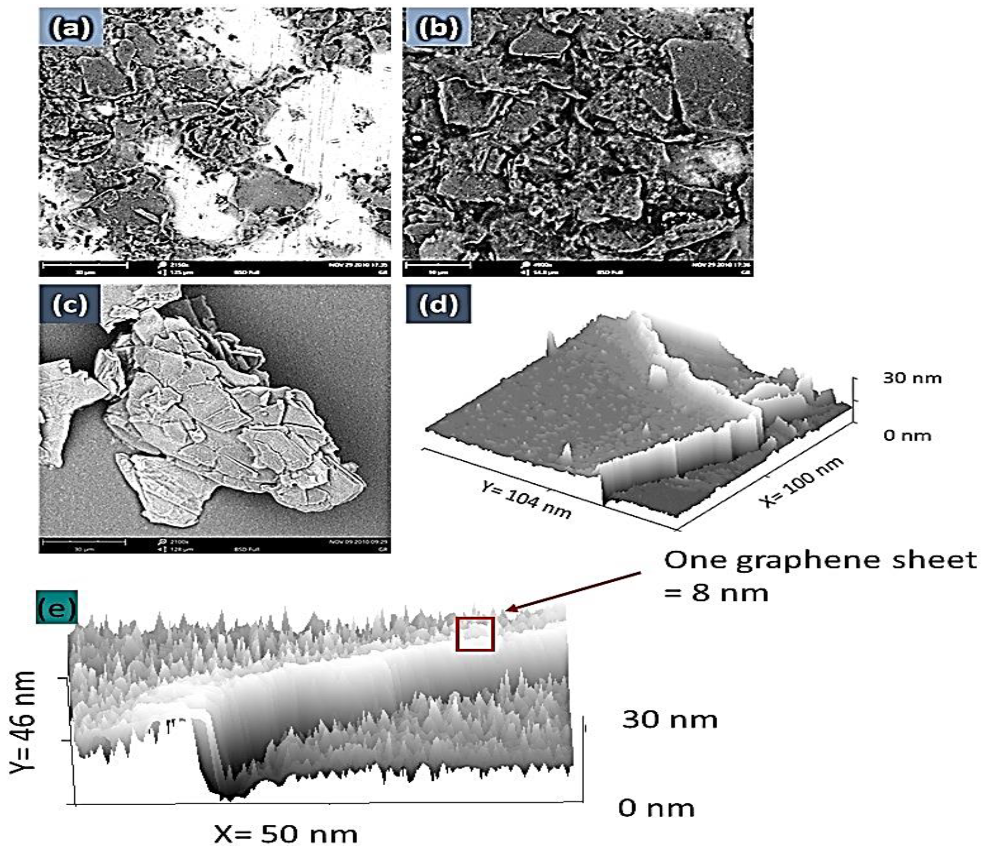
Within this context, the electrophoretic deposition (EPD) method emerges as a significant transformative process. Its merits lie in its ability to achieve a uniform deposition of 2D materials, resulting in a continuous arrangement of laterally connected nanosheets. This accomplishment is beautifully visualized in Figure 3a–c, wherein a grid-like structure (GLS) of the thin film is displayed. This structure is distinguished by a remarkable degree of flatness—an attribute critical for enabling high-speed electron mobility.
A cross-sectional perspective of the deposited graphene film, as portrayed in Figure 3c,d, reveals an approximate thickness of 70 nm. This insight into the film’s structural dimensionality is invaluable, contextualizing its performance within various applications.

3.1.1. Discussion

The resounding success of the EPD technique, exemplified in the grid-like structure (GLS) of the thin film (Figure 3), underscores its transformative potential in graphene film production. The high degree of flatness exhibited by this film holds crucial importance, particularly in applications demanding high-speed electron mobility. This attribute is vital for optimizing the film’s electronic performance, amplifying its potential in diverse electronic and optoelectronic devices.
The cross-sectional image’s revelation of a graphene film thickness of approximately 70 nm provides a quantitative understanding of the film’s structural dimensionality. This knowledge enables a deeper appreciation of its suitability for specific applications, especially those that require materials of defined thicknesses to achieve desired functionalities.
The uniformity of the deposited graphene film is further explored through EDAX elemental mapping analysis, showcased in Figure 4a,b for white and color. The affirmation of a high degree of uniformity within the deposited film offers compelling validation of the EPD technique’s prowess in crafting high-quality, uniform 2D material films. This observation reinforces the transformative potential of EPD in producing materials with consistent and controlled properties, poised to unlock new horizons in various technological domains.

3.1.2. Results and Discussion: X-ray Diffraction

The detailed analysis presented in this section sheds further light on the outstanding quality and structural characteristics of the synthesized graphene nanosheets (graphene NSs).
Figure 5a brings attention to the X-ray diffraction (XRD) pattern of the graphene nanosheets, highlighting their crystalline nature. The presence of two prominent peaks at 2θ angles of 25.3° and 47°, corresponding to the (002) and (100) crystallographic planes of graphene’s structure, respectively, provides compelling insights. The (002) peak arises from the constructive interference of X-rays scattered by carbon atoms within the parallel stacked graphene layers. This peak’s position and intensity offer a means to gauge the interlayer spacing, which typically measures around 0.34 nm for graphene. The presence of a distinct (100) peak signifies the orientation and arrangement of carbon atoms within the graphene plane and can be indicative of the material’s degree of crystallinity. Notably, the XRD pattern in Figure 5a unveils a pronounced alignment with the (002) and (100) crystallographic planes, indicative of a high level of crystallinity and a well-defined crystal structure. This aligns coherently with high-quality graphene samples, often characterized by sharp and well-defined XRD peaks [27].
Moving on to Figure 5b, we delve into the Raman spectrum of the graphene sheets, where we observe the emergence of G, D’, and 2D peaks [28]. The G peak, resonating at 1580 cm−1, originates from E2g phonons at the Brillouin zone and signifies the in-plane stretching vibrations of sp2-bonded carbon atoms. The position of this G peak is known to be influenced by the number of graphene layers, exhibiting a blue shift as the layer count increases—a phenomenon rooted in varying dimer interactions across different layer counts. Remarkably, the number of layers present can be deduced using Equation (1):
ω G = 1581.6 + 11 ( 1 + n 1.6 )
where ωG is the band position, and n is the number of layers.
Notably, the Raman spectrum analysis of the graphene sheets reveals the presence of a G peak at 1580 cm−1, indicative of in-plane stretching vibrations of sp2-bonded carbon atoms, suggesting the presence of approximately four layers of graphene [29,30].
Further insights arise with the identification of the defect mode D’ at 1620 cm−1 and the 2D peaks, corresponding to the two phonons TO at the K-point, situated around 3000 cm−1, confirming the formation of graphene nanosheets. The appearance of the 2D peak at about 3000 cm−1 in the Raman spectra serves as definitive evidence of the presence of graphene nanosheets within our thin films [31].
A particularly pertinent discovery emerges from the well-defined and narrow 2D peak, indicating the likelihood of few-layer or monolayer graphene possessing enhanced electronic and mechanical properties. This observation underscores the high structural order and reduced defect density, both vital attributes for optimizing photovoltaic device performance [32,33,34,35,36,37].
The comprehensive results of this characterization unveil the prowess of the electrophoretic deposition (EPD) technique as a cost-effective, straightforward, and efficient method for fabricating high-quality, flat, and uninterrupted thin graphene films derived from suspended nanosheets. This combination of high structural integrity, uniformity, and crystallinity propels graphene’s applicability in various technological realms, setting the stage for innovative advancements.

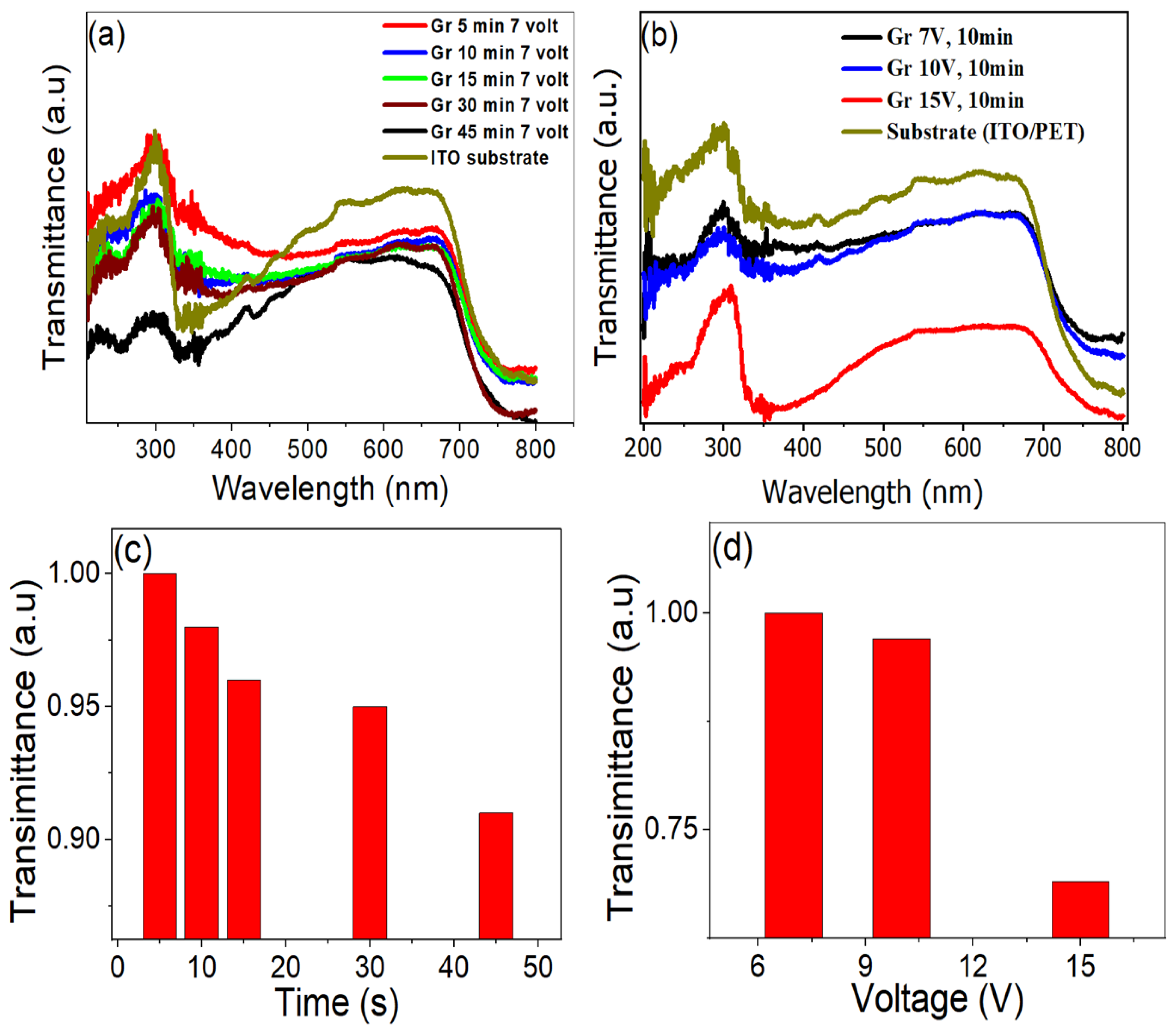
3.1.3. Results and Discussion—UV–Vis Spectra Analysis

The exploration of thin film transparency, formed through the deposition of graphene nanosheets dispersed in ethanol, was undertaken through an analysis of their UV–Vis spectra. This examination yields critical insights into the optical properties of graphene films, paving the way for their application in various optoelectronic devices.
In Figure 6, we observe the transmittance spectra of graphene films deposited at a constant voltage of 7 V and room temperature (25 °C) across different deposition times ranging from 5 to 45 min. As depicted in Figure 6a, it is evident that film transparency decreases with an increase in deposition time. This intricate interplay highlights the dynamic nature of the fabrication process.
Figure 6c provides a comprehensive view of the relationship between transmittance values and deposition time for graphene nanosheets deposited under varying voltage conditions (ranging from 7 V to 15 V). Notably, with an increase in voltage during the deposition process, a corresponding decrease in resultant film transparency is observed (Figure 6b). This phenomenon is further emphasized in Figure 6d, derived from Figure 6b, offering a concise visualization of the interaction between applied voltage and film transparency. These findings signify that the transparency of deposited films can be skillfully controlled by adjusting deposition time and applied voltage within the electrophoretic deposition (EPD) process.
The unique optical characteristics of graphene nanosheets have ignited a wide range of applications spanning from ultraviolet (UV) to infrared (IR). Their exceptional transparency and conductivity make them ideal candidates for applications like transparent conductive films, touchscreens, and solar cells [38,39,40,41,42,43]. Additionally, their suitability as photodetectors due to high responsivity, rapid response times, and a broad spectral range is noteworthy [44,45,46,47,48]. Graphene nanosheets also excel as saturable absorbers in mode-locked lasers, opening avenues for generating ultrashort pulses in the femtosecond regime [49,50]. Moreover, their pronounced interaction with light in the IR region positions them as promising materials for infrared sensors [51]. This diverse range of capabilities extends to the use of graphene nanosheets in the development of optical modulators, waveguides, and biosensors [52]. Therefore, the broad absorbance range of graphene nanosheets, covering from UV to IR, coupled with their distinct electrical and mechanical properties, establishes them as highly sought-after materials across a wide array of optoelectronic applications.

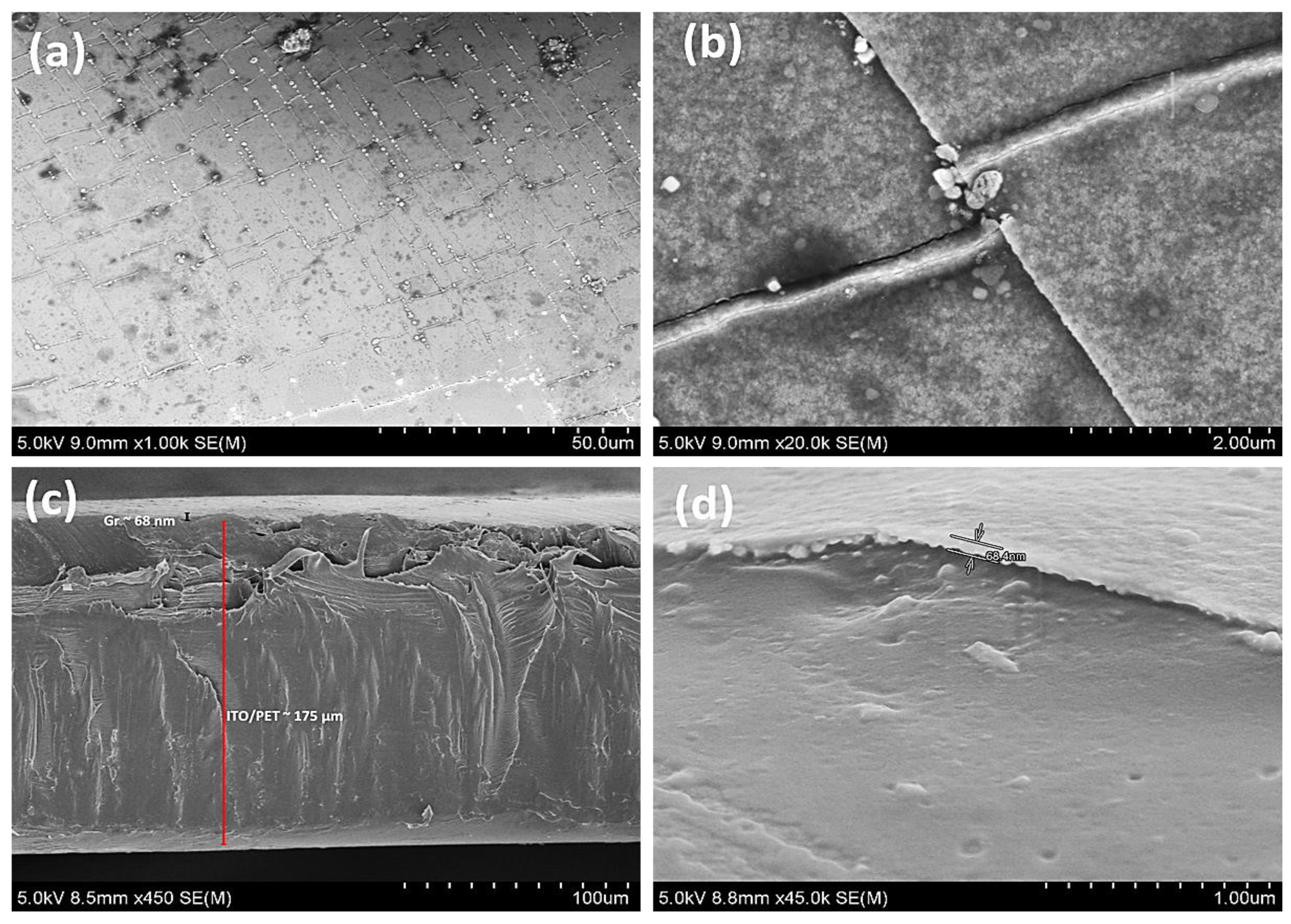
3.2. Monitoring the Deposition Process

Gaining insight into the behavior of charged graphene sheets during the deposition process is crucial for unraveling the intricacies of the process dynamics. To comprehensively understand this phenomenon, diligent monitoring of the total charge carried by the suspended sheets under the influence of an applied electrical field is imperative; this charge is commonly referred to as the tracked current.
The insights obtained from this monitoring process are vividly illustrated in Figure 7. Here, the tracked current is graphically represented as a function of time across varying applied voltages, also known as electromotive force (EMF). The results of this analysis reveal a fascinating relationship between applied voltage and the number of charged sheets deposited onto the conductive substrate. Specifically, as the applied voltage increases from 5 V to 10 V, there is a corresponding rise in the number of charged sheets deposited, resulting in a remarkable surge in the charge current—transitioning from a modest 10 µA to an impressive over 25 µA.
Furthermore, it is worth noting that the graphene nanosheets display distinctive peaks in their behavior. Two peaks, notably occurring at around 30 s and 130 s, emerge as significant landmarks. These peaks provide a captivating insight into the deposition mechanism, suggesting a layered approach wherein the deposition of graphene layers on the conductive substrate takes place, setting the stage for subsequent layers of graphene.
The revelations stemming from this meticulous analysis add substantial value to the comprehension of the deposition mechanism. This deeper understanding has the potential to catalyze the optimization of the electrophoretic deposition (EPD) process, ultimately facilitating the creation of highly uniform and meticulously controlled graphene thin films. These insights mark a pivotal step forward in harnessing the potential of graphene nanosheets for a spectrum of applications.

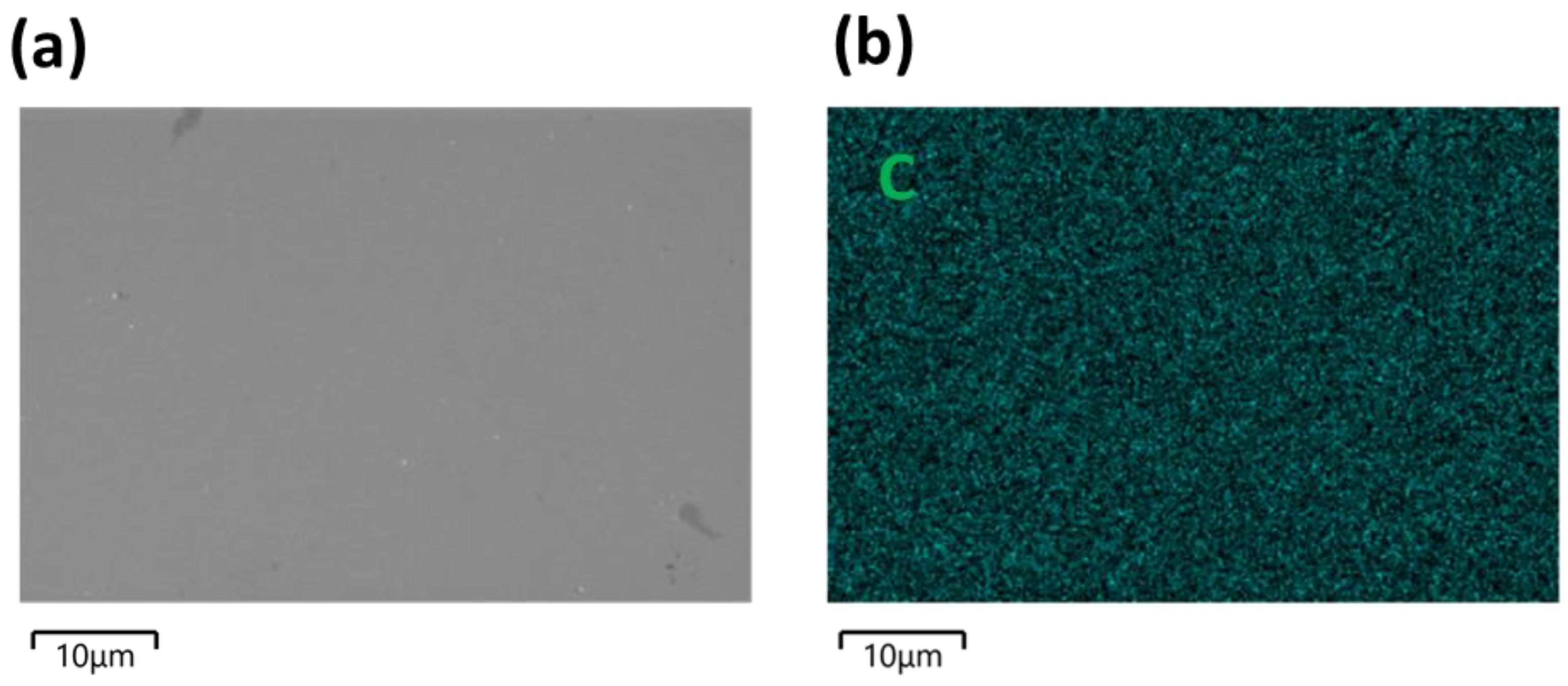
3.3. Analyzing Charged Graphene Sheets in the Deposition Process

This analysis delves into the behavior of charged graphene sheets during the deposition process, providing valuable insights into the intricate current dynamics underlying the electrophoretic deposition (EPD) technique.
(a) The tracked current is plotted against time, illustrating how different applied voltages (electromotive force, EMF) influence current behavior. This representation offers a comprehensive overview of the impact of varying EMFs on the deposition process.
(b) Noticeable trends emerge as applied voltage increases from 5 V to 10 V. With higher applied voltage, there is a corresponding increase in the number of charged graphene sheets deposited onto the conductive substrate. Consequently, a substantial surge in the charge current occurs, with values escalating from a modest 10 µA to an impressive over 25 µA.
(c) Intriguingly, graphene nanosheets exhibit distinctive peaks in their behavior. These peaks, particularly prominent around 30 s and 130 s, provide pivotal insights into the deposition mechanism. Their occurrence suggests a layered deposition approach, wherein graphene layers are successively added to the conductive substrate, establishing the foundation for subsequent layers of graphene.
This detailed analysis not only enhances our understanding of the deposition mechanism but also paves the way for optimizing the EPD process. The implications of these findings extend to the creation of highly uniform and precisely controlled graphene thin films, enriching the potential applications of graphene nanosheets across diverse domains.

4. Conclusions

In conclusion, the electrophoretic deposition (EPD) technique proves to be a promising method for large-scale graphene fabrication. We have meticulously deposited thin graphene films using this method and extensively characterized them using FESEM, EDAX elemental mapping, XRD, and Raman analysis.
X-ray diffraction (XRD) confirms the crystalline structure of graphene with characteristic peaks at 25.3 and 47°. Raman analysis reveals the presence of the G peak at 1580 cm−1, indicating high-quality graphene.
Our exploration of the optical properties of graphene nanosheets (G-NSs) unveiled intriguing trends. Transmittance decreases with longer deposition times and higher applied voltages, leading to increased charge current.
This innovative approach not only advances graphene production but also provides valuable insights into controlling the optical properties of thin films during deposition. The precise control of film thickness and optical characteristics makes these 2D graphene NS films ideal for various applications, including optoelectronics, energy storage, sensing, and quantum technologies [53].

Author Contributions

Methodology, A.A.A.A.; formal analysis, A.A.A.A., A.B.G.T., F.H.A. and M.R.; investigation, A.A.A.A., A.B.G.T., F.H.A., S.A., M.S., T.A.A., K.S.A., F.V.K. and M.R. supervision, A.B.G.T., F.H.A., S.A., M.S., T.A.A., K.S.A., F.V.K. and M.R.; writing—original draft preparation, A.A.A.A., A.B.G.T., F.H.A., F.V.K. and M.R.; writing—review and editing, A.A.A.A., A.B.G.T., F.H.A., F.V.K. and M.R.; funding acquisition, A.B.G.T. and F.H.A. All authors have read and agreed to the published version of the manuscript.

Funding

This work was funded by the Deanship of Scientific Research at Princess Nourah bint Abdulrahman University through the Research Groups Program Grant No. (RGP-1442-0034).

Institutional Review Board Statement

Not applicable.

Informed Consent Statement

Not applicable.

Data Availability Statement

Not applicable.

Acknowledgments

The authors express their gratitude to the Deanship of Scientific Research at Princess Nourah bint Abdulrahman University through the Research Groups Program Grant No. (RGP-1442-0034).

Conflicts of Interest

The authors declare no conflict of interest.

References

  1. Geim, A.k.; Novoselov, K.S. The rise of graphene, Nanoscience and technology: A collection of reviews. Nature 2010, 1, 11–19. [Google Scholar]
  2. Coleman, J.N.; Lotya, M.; O’Neill, A.; Bergin, S.D.; King, P.J.; Khan, U.; Young, K.; Gaucher, A.; De, S.; Smith, R.J. Two-dimensional nanosheets produced by liquid exfoliation of layered materials. Science 2011, 331, 568–571. [Google Scholar] [CrossRef]
  3. Li, X.; Tao, L.; Chen, Z.; Fang, H.; Li, X.; Wang, X.; Xu, J.-B.; Zhu, H. Graphene and related two-dimensional materials: Structure-property relationships for electronics and optoelectronics. Appl. Phys. Rev. 2017, 4, 021306. [Google Scholar] [CrossRef]
  4. Wang, J.S.; Cao, Y.; Ding, F.; Ma, W.; Sun, M. Theoretical investigations of optical origins of fluorescent graphene quantum dots. Sci. Rep. 2016, 6, 1–5. [Google Scholar] [CrossRef]
  5. Whitener, K.E., Jr.; Sheehan, P.E. Graphene synthesis. Diam. Relat. Mater. 2014, 46, 25–34. [Google Scholar] [CrossRef]
  6. Charrier, A.; Coati, A.; Argunova, T.; Thibaudau, F.; Garreau, Y.; Pinchaux, R.; Forbeaux, I.; Debever, J.M.; Sauvage-Simkin, M.; Themlin, J.M. Solid-state decomposition of silicon carbide for growing ultra-thin heteroepitaxial graphite films. J. Appl. Phys. 2002, 92, 2479–2484. [Google Scholar] [CrossRef]
  7. Berger, C.; Song, Z.; Li, T.; Li, X.; Ogbazghi, A.Y.; Feng, R.; Dai, Z.; Marchenkov, A.N.; Conrad, E.H.; First, P.N. Ultrathin epitaxial graphite: 2D electron gas properties and a route toward graphene-based nanoelectronics. J. Phys. Chem. B 2004, 108, 19912–19916. [Google Scholar] [CrossRef]
  8. Berger, C.; Song, Z.; Li, X.; Wu, X.; Brown, N.; Naud, C.; Mayou, D.; Li, T.B.; Hass, J.; Marchenkov, A.N.; et al. Electronic confinement and coherence in patterned epitaxial graphene. Science 2006, 312, 1191–1196. [Google Scholar] [CrossRef] [PubMed]
  9. Wang, X.; Shi, G. An introduction to the chemistry of graphene. Phys. Chem. Chem. Phys. 2015, 17, 28484–28504. [Google Scholar] [CrossRef]
  10. Li, D.; Müller, M.B.; Gilje, S.; Kaner, R.B.; Wallace, G.G. Processable aqueous dispersions of graphene nanosheets. Nat. Nanotechnol. 2008, 3, 101–105. [Google Scholar] [CrossRef]
  11. Shan, C.; Yang, H.; Han, D.; Zhang, Q.; Ivaska, A.; Niu, L. Water-soluble graphene covalently functionalized by biocompatible poly-L-lysine. Langmuir 2009, 25, 12030–12033. [Google Scholar] [CrossRef] [PubMed]
  12. Coleman, J.N. Liquid-Phase Exfoliation of Nanotubes and Graphene. Adv. Funct. Mater. 2009, 19, 3680–3695. [Google Scholar] [CrossRef]
  13. Hernandez, Y.; Nicolosi, V.; Lotya, M.; Blighe, F.M.; Sun, Z.; De, S.; McGovern, I.T.; Holland, B.; Byrne, M.; Gun’Ko, J.K.; et al. High-yield production of graphene by liquid-phase exfoliation of graphite. Nat. Nanotechnol. 2008, 3, 563–568. [Google Scholar] [CrossRef] [PubMed]
  14. Mushfiq, S.W.; Afzalzadeh, R. Verification of experimental results with simulation on production of few-layer graphene by liquid-phase exfoliation utilizing sonication. Sci. Rep. 2022, 12, 9872. [Google Scholar] [CrossRef] [PubMed]
  15. Rabiei Baboukani, A.; Khakpour, I.; Drozd, V.; Wang, C. Liquid-Based Exfoliation of Black Phosphorus into Phosphorene and Its Application for Energy Storage Devices. Small Struct. 2021, 2, 2000148. [Google Scholar] [CrossRef]
  16. Baboukani, A.R.; Khakpour, I.; Drozd, V.; Allagui, I. Single-step exfoliation of black phosphorus and deposition of phosphorene via bipolar electrochemistry for capacitive energy storage application. J. Mater. Chem. A 2019, 7, 25548–25556. [Google Scholar] [CrossRef]
  17. Cayambe, M.; Zambrano, C.; Tene, T.; Guevara, M.; Tubon Usca, G.; Brito, H.; Molina, R.; Coello-Fiallos, D.; Caputi, L.S.; Vacacela Gomez, C. Dispersion of graphene in ethanol by sonication. Mater. Today Proc. 2021, 37, 4027–4030. [Google Scholar] [CrossRef]
  18. Vacacela Gomez, C.; Tene, T.; Guevara, M.; Tubon Usca, G.; Colcha, D.; Brito, H.; Molina, R.; Bellucci, S.; Tavolaro, A. Preparation of few-layer graphene dispersions from hydrothermally expanded graphite. Appl. Sci. 2019, 9, 2539. [Google Scholar] [CrossRef]
  19. Usca, G.T.; Hernandez-Ambato, J.; Pace, C.; Caputi, L.; Tavolaro, A. Liquid-phase exfoliated graphene self-assembled films: Low-frequency noise and thermal-electric characterization. Appl. Surf. Sci. 2016, 380, 268–273. [Google Scholar] [CrossRef]
  20. Dang, T.T.; Pham, V.H.; Hur, S.H.; Kim, E.J.; Kong, B.-S.; Chung, J.S. Superior dispersion of highly reduced graphene oxide in N, N-dimethylformamide. J. Colloid Interface Sci. 2012, 376, 91–96. [Google Scholar] [CrossRef]
  21. Akhavan, O. The effect of heat treatment on formation of graphene thin films from graphene oxide nanosheets. Carbon 2010, 48, 509–519. [Google Scholar] [CrossRef]
  22. Kim, J.; Ganorkar, S.; Kim, Y.-H.; Kim, S.-I. Graphene oxide hole injection layer for high-efficiency polymer light-emitting diodes by using electrophoretic deposition and electrical reduction. Carbon 2015, 94, 633–640. [Google Scholar] [CrossRef]
  23. Neirinck, B.; Fransaer, J.; Van der Biest, O.; Vleugels, O. Aqueous electrophoretic deposition in asymmetric AC electric fields (AC–EPD). Electrochem. Commun. 2009, 11, 57–60. [Google Scholar] [CrossRef]
  24. Wang, M.; Oh, J.; Ghosh, T.; Hong, S.; Nam, G.; Hwang, T.; Nam, J.-D. An interleaved porous laminate composed of reduced graphene oxide sheets and carbon black spacers by in situ electrophoretic deposition. RSC Adv. 2014, 4, 3284–3292. [Google Scholar] [CrossRef]
  25. Oh, J.-S.; Kim, S.-H.; Hwang, T.; Kwon, H.-Y.; Lee, T.H.; Bae, A.-H.; Choi, H.R.; Nam, J.-D. Laser-assisted simultaneous patterning and transferring of graphene. J. Phys. Chem. C 2013, 117, 663–668. [Google Scholar] [CrossRef]
  26. Yang, Y.; Wei, Y.; Guo, Z.; Hou, W.; Liu, Y.; Tian, H.; Ren, T.L. From Materials to Devices: Graphene toward Practical Applications. Small Methods 2022, 6, 2200671. [Google Scholar] [CrossRef]
  27. Helmy, A.; Rabia, M.; Shaban, M.; Ashraf, A.M.; Ahmed, S.; Ahmed, A.M. Graphite/Rolled Graphene Oxide/Carbon Nanotube Photoelectrode for Water Splitting of Exhaust Car Solution. Int. J. Energy Res. 2020, 44, 7687–7697. [Google Scholar] [CrossRef]
  28. Lv, R.; Terrones, M. Towards new graphene materials: Doped graphene sheets and nanoribbons. Mater. Lett. 2012, 78, 209–218. [Google Scholar] [CrossRef]
  29. Wang, H.; Wang, Y.; Cao, X.; Feng, M.; Lan, G. Vibrational properties of graphene and graphene layers. J. Raman Spectrosc. 2009, 40, 1791–1796. [Google Scholar] [CrossRef]
  30. Ghosh, S.; Nika, D.; Pokatilov, E.A. Balandin, Heat conduction in graphene: Experimental study and theoretical interpretation. N. J. Phys. 2009, 11, 095012. [Google Scholar] [CrossRef]
  31. Johra, F.T.; Lee, J.W.; Jung, W.G. Facile and Safe Graphene Preparation on Solution Based Platform. J. Ind. Eng. Chem. 2014, 20, 2883–2887. [Google Scholar] [CrossRef]
  32. Shaban, M.; Rabia, M.; Eldakrory, M.G.; Maree, R.M.; Ahmed, A.M. Efficient Photoselectrochemical Hydrogen Production Utilizing of APbI3 (A = Na, Cs, and Li) Perovskites Nanorods. Int. J. Energy Res. 2021, 45, 7436–7446. [Google Scholar] [CrossRef]
  33. Abdelazeez, A.A.A.; Trabelsi, A.B.G.; Alkallas, F.H.; Rabia, M. Successful 2D MoS2 Nanosheets Synthesis with SnSe Grid-like Nanoparticles: Photoelectrochemical Hydrogen Generation and Solar Cell Applications. Sol. Energy 2022, 248, 251–259. [Google Scholar] [CrossRef]
  34. Alkallas, F.H.; Elsayed, A.M.; Trabelsi, A.B.G.; Rabia, M. Quantum Dot Supernova-like-Shaped Arsenic (III) Sul-fide-Oxide/Polypyrrole Thin Film for Optoelectronic Applications in a Wide Optical Range from Ultraviolet to In-frared. Catalysts 2023, 13, 1274. [Google Scholar] [CrossRef]
  35. Shaban, M.; Rabia, M.; Fathallah, W.; El-Mawgoud, N.A.; Mahmoud, A.; Hussien, H.; Said, O. Preparation and Characterization of Polyaniline and Ag/Polyaniline Composite Nanoporous Particles and Their Antimicrobial Activities. J. Polym. Environ. 2017, 26, 434–442. [Google Scholar] [CrossRef]
  36. Abdelazeez, A.A.A.; Hadia, N.M.A.; Mourad, A.H.I.; El-Fatah, G.A.; Shaban, M.; Ahmed, A.M.; Alzaid, M.; Cherupurakal, N.; Rabia, M. Effect of Au Plasmonic Material on Poly M-Toluidine for Photoelectrochemical Hydrogen Generation from Sewage Water. Polymers 2022, 14, 768. [Google Scholar] [CrossRef] [PubMed]
  37. Rabia, M.; Shaban, M.; Jibali, B.M.; Abdelkhaliek, A.A. Effect of Annealing Temperature on the Photoactivity of ITO/VO 2 (M)/Au Film Electrodes for Water Splitting. J. Nanosci. Nanotechnol. 2020, 20, 4120–4130. [Google Scholar] [CrossRef]
  38. Michael, L.; Kamyshny, A.; Magdassi, S. Transparent conductors composed of nanomaterials. Nanoscale 2014, 11, 5581–5591. [Google Scholar]
  39. Qingbin, Z. Graphene oxide-based transparent conductive films. Prog. Mater. Sci. 2014, 64, 200–247. [Google Scholar]
  40. Shaban, M.; Ali, S.; Rabia, M. Design and Application of Nanoporous Graphene Oxide Film for CO2, H2, and C2H2 Gases Sensing. J. Mater. Res. Technol. 2019, 8, 4510–4520. [Google Scholar] [CrossRef]
  41. Shuping, P. Graphene as transparent electrode material for organic electronics. Adv. Mater. 2011, 23, 2779–2795. [Google Scholar]
  42. Francesco, B. Graphene photonics and optoelectronics. Nat. Photonics 2010, 4, 611–622. [Google Scholar]
  43. Xiao, H. Graphene-based electrodes. Adv. Mater. 2012, 24, 5979–6004. [Google Scholar]
  44. Wengang, L. Gate tuning of high-performance InSe-based photodetectors using graphene electrodes. Adv. Opt. Mater. 2015, 3, 1418–1423. [Google Scholar]
  45. Di, W. Highly polarization-sensitive, broadband, self-powered photodetector based on graphene/PdSe2/germanium heterojunction. ACS Nano 2019, 13, 9907–9917. [Google Scholar]
  46. Hui, Q. Self-powered photodetectors based on 2D materials. Adv. Opt. Mater. 2020, 8, 1900765. [Google Scholar]
  47. Jacobs-Gedrim, R.B. Extraordinary photo response in two-dimensional In2Se3 nanosheets. ACS Nano 2014, 8, 514–521. [Google Scholar] [CrossRef]
  48. Ben Gouider, A.B. Morphological imperfections of epitaxial graphene: From a hindrance to the generation of new photo-responses in the visible domain. Nanoscale 2017, 9, 11463–11474. [Google Scholar] [CrossRef]
  49. Ursula, K. Semiconductor saturable absorber mirrors (SESAM’s) for femtosecond to nanosecond pulse generation in solid-state lasers. IEEE J. Sel. Top. Quantum Electron. 1996, 2, 435–453. [Google Scholar]
  50. Binglei, Z. Photon Drag Currents and Terahertz Generation in α-Sn/Ge Quantum Wells. Nanomaterials 2022, 12, 2892. [Google Scholar]
  51. Isaac, L. Graphene–metamaterial photodetectors for integrated infrared sensing. ACS Photonics 2016, 3, 936–941. [Google Scholar]
  52. Konstantin, S.N. A roadmap for graphene. Nature 2012, 490, 192–200. [Google Scholar]
  53. Forrester, D.M.; Kusmartsev, F.V. Electron quantum optics with beam splitters and waveguides in dirac matter. Adv. Quantum Technol. 2023, 6, 2300112. [Google Scholar] [CrossRef]
Figure 1. Fabrication process for graphene nanosheets (G-NSs) on an ITO/PET substrate. The process begins with the creation of a G-NS suspension in ethanol using the liquid-phase exfoliation (EPD) technique. Subsequent refinement of the resulting dispersion is achieved through centrifugation and electrophoretic deposition (EPD).
Coatings 13 01628 g001
Figure 2. (ac) SEM images depicting graphene nanosheets on a mica substrate, employing the drop-casting technique; (d,e) plots highlighting the unique 2D structure of graphene nanosheets with a flat morphology.
Coatings 13 01628 g002
Figure 3. (a) Low magnification FE-SEM image of graphene film deposited on ITO/PET conductive substrate with a high degree of flatness; (b,c) high and low magnification FE-SEM images of the graphene NS with a thickness of ~67 nm, respectively; (d) high magnification FE-SEM image the graphene electrophoretic deposited thin film cross-section (~70 nm) on the surface of ITO/PET substrate.
Coatings 13 01628 g003
Figure 4. EDAX elemental mapping area for graphene NS thin films (a) white and (b) color.
Coatings 13 01628 g004
Figure 5. Characterization of graphite and graphene: (a) Microscopic image showcasing the crystalline structure of graphite as a bulk material, providing insight into its macroscopic arrangement. (b) X-ray diffraction (XRD) pattern of the graphite powder sample, offering valuable information about the crystalline arrangement and atomic spacing within the material. (c) Comparative XRD analysis, demonstrating the crystalline structure of the graphene film formed in two dimensions, highlighting its unique properties in contrast to bulk graphite. (d) Raman analysis of the 2D graphene film, offering insights into its vibrational modes and confirming the formation of the graphene structure.
Coatings 13 01628 g005
Figure 6. UV–Vis spectra of graphene thin films: (a) Transmittance spectra of graphene thin films deposited for different durations (5–45 min) under constant temperature conditions (room temperature 25 °C) and voltage (7 V). (b) Transmittance spectra of graphene thin films deposited under different voltage settings (7–15 V) for a consistent deposition time (10 min) and room temperature. (c) Relationship between deposition time and transmittance, demonstrating the impact of time on transmittance under various deposition durations. (d) Relationship between deposition voltage and transmittance, illustrating the effect of voltage variation on transmittance for different deposition voltages.
Coatings 13 01628 g006
Figure 7. Tracked current analysis during graphene NS deposition process.
Coatings 13 01628 g007
Disclaimer/Publisher’s Note: The statements, opinions and data contained in all publications are solely those of the individual author(s) and contributor(s) and not of MDPI and/or the editor(s). MDPI and/or the editor(s) disclaim responsibility for any injury to people or property resulting from any ideas, methods, instructions or products referred to in the content.

