Article

Tunable Electronic and Optical Properties of MoGe2N4/AlN and MoSiGeN4/AlN van der Waals Heterostructures toward Optoelectronic and Photocatalytic Applications

1
Jiangxi Provincial Key Laboratory for Simulation and Modelling of Particulate Systems, School of Energy and Mechanical Engineering, Jiangxi University of Science and Technology, Nanchang 330013, China
2
Key Laboratory for Micro-Nano Optoelectronic Devices of Ministry of Education, School of Physics and Electronics, Hunan University, Changsha 410082, China
3
Centre for Infrastructure Engineering, School of Engineering, Design and Built Environment, Western Sydney University, Penrith, NSW 2751, Australia
*
Authors to whom correspondence should be addressed.
Coatings 2024, 14(4), 500; https://doi.org/10.3390/coatings14040500
Submission received: 24 March 2024 / Revised: 13 April 2024 / Accepted: 15 April 2024 / Published: 18 April 2024
(This article belongs to the Special Issue Advances in Two-Dimensional Materials: From Synthesis to Applications)

Abstract

:
Van der Waals (vdW) heterostructures provide an effective strategy for exploring and expanding the potential applications of two-dimensional materials. In this study, we employ first-principles density functional theory (DFT) to investigate the geometric, electronic, and optical properties of MoGe2N4/AlN and MoSiGeN4/AlN vdW heterostructures. The stable MoGe2N4/AlN heterostructure exhibits an indirect band gap semiconductor with a type-I band gap arrangement, making it suitable for optoelectronic devices. Conversely, the stable MoSiGeN4/AlN heterostructure demonstrates various band gap arrangements depending on stacking modes, rendering it suitable for photocatalysis applications. Additionally, we analyze the effects of mechanical strain and vertical electric field on the electronic properties of these heterostructures. Our results indicate that both mechanical strain and vertical electric field can adjust the band gap. Notably, application of an electric field or mechanical strain leads to the transformation of the MoGe2N4/AlN heterostructure from a type-I to a type-II band alignment and from an indirect to a direct band transfer, while MoSiGeN4/AlN can transition from a type-II to a type-I band alignment. Type-II band alignment is considered a feasible scheme for photocatalysis, photocells, and photovoltaics. The discovery of these characteristics suggests that MoGe2N4/AlN and MoSiGeN4/AlN vdW heterostructures, despite their high lattice mismatch, hold promise as tunable optoelectronic materials with excellent performance in optoelectronic devices and photocatalysis.

1. Introduction

Environmental pollution poses significant threats to human survival and development as it continues to escalate. The depletion of carbon-based fossil fuels, along with their increasing consumption, highlights the urgent need for renewable energy alternatives with exceptional performance. Consequently, there is ongoing exploration of novel materials and technologies to address these pressing needs [1]. Notably, since 2004, the successful isolation of graphene from three-dimensional materials has marked the beginning of a new era in two-dimensional nanomaterial research [2]. Building upon this breakthrough, new two-dimensional materials have been continuously produced and studied, including graphene, hexagonal boron nitride (h-BN), and transition metal dichalcogenides (TMDs), among others [3,4,5,6,7]. Moreover, van der Waals (vdW) heterostructures, formed by vertically stacking two-dimensional layered materials, have been extensively explored in theory and experiment [8]. Based on the alignment of the conduction and valence bands of two materials, two-dimensional semiconductor van der Waals heterostructures can be categorized into three types: type-I (straddling gap) heterojunctions, where both the Valence Band Maximum (VBM) and the Conduction Band Minimum (CBM) are located within the same semiconductor material, type-II (staggered gap) heterojunctions, in which the VBM and CBM originate from different semiconductors, and type-III (broken gap) heterojunctions, where there is an energy crossover between the VBM and CBM [8,9,10,11,12]. Therefore, combining different single-layer two-dimensional materials in a composite structure may yield structural, electronic, and optical properties superior to those of isolated materials, thus significantly expanding the design space and functionality of two-dimensional materials. These advancements play a crucial role in catalysis, optoelectronic detection, and optoelectronic devices [13,14,15,16,17,18].
Additionally, two-dimensional AlN can be successfully prepared between graphene and Si substrates using metal organic chemical vapor deposition (MOCVD) technology, exhibiting a planar hexagonal structure similar to graphene [19,20,21,22,23,24,25,26]. Research indicates that AlN holds enormous potential for application in optical devices owing to its ability to absorb photons in the ultraviolet and visible light ranges [27]. However, its large indirect bandgap, lower carrier mobility, and poor photoelectric response performance pose obstacles to its broader utilization [28]. Fortunately, the construction of a vdW heterostructure offers the possibility of breakthrough performance. For instance, studies have shown that AlN/MoSe2 and AlN/WS2 heterostructures all exhibit band gaps suitable for photocatalytic water splitting [29].
Moreover, recent advancements in materials synthesis have led to the production of a novel centimeter-level single-layer MoSi2N4 thin film with excellent performance via chemical vapor deposition [27,30,31]. This development holds significant promise for future nanodevices and catalysis applications. Additionally, the exploration of the two-dimensional MA2X4 material family—where M = Mo, W, V, Nb, Ta, Ti, Zr, Hf, or Cr, A = Si or Ge, and X = N, P, or As—has sparked considerable research interest [32,33]. Notably, the prediction of a new Janus MoSiGeN4 monolayer film with good stability, a suitable band edge position, and excellent light absorption ability suggests potential applications in various fields [34,35,36,37,38,39]. Nguyen et al. reported the use of graphene and MoSiGeN4 to form heterostructures to prepare high-performance nanoelectronic devices [40]. Lv et al. studied the structural and electronic properties of different stacking configurations of double-layer MoSiGeN4 and achieved a type-II alignment electronic structure through the built-in electric field [41]. Wang et al. reported the use of the MoGe2N4/MoSTe heterostructure as a promising tunable optoelectronic material [42]. Inspired by the above content, we decided to combine MoSiGeN4/MoGe2N4 with AlN to construct heterostructures and study the changes in their electronic properties through biaxial strain and a vertical electric field.
Therefore, for the purpose of this paper, MoGe2N4/AlN and MoSiGeN4/AlN vdW heterostructures were constructed. Each heterostructure adopts six different high-symmetry stacking modes. The geometric structure and electronic properties of AlN, MoSiGeN4, and MoGe2N4 monolayers were verified by density functional theory (DFT). It was found that MoGe2N4/AlN exhibits different band gap arrangements in different stacking modes, while MoSiGeN4/AlN was identified as a type-I heterostructure, suitable for optoelectronic devices. Subsequently, we tuned the electronic properties of the heterostructure through biaxial strain and electric field. The results demonstrate that the band gap energy can be effectively adjusted under the influence of plane biaxial strain and electric field while maintaining the intrinsic type-II band alignment. This work contributes to further advancements in the research of MA2Z4 family materials and showcases their potential applications in optoelectronic and nanoelectronic devices, offering significant value for practical applications.

2. Computational Methodology

The first-principles calculations based on density functional theory (DFT) were performed using the Vienna ab initio simulation package (VASP) [43,44,45]. The Perdew–Burke–Ernzerhof (PBE) generalized gradient approximation (GGA) was used to describe the electron exchange and related information. The projection enhanced wave method of plane wave basis set was used to describe the interaction between electrons and ions [46,47]. The weak vdW force between layers was corrected using the empirical correction method of grimme (DFT-D3) [48]. We also solve the problem of band gap underestimation by comparing the more accurate electronic properties of the 2006 HSE06 hybrid functional with the PBE method [49]. The energy cut-off value was set to 500 eV. The Brillouin zone was calculated using the Monkhorst–Pack k point grid 9 × 9 × 1 . The structural relaxation was calculated using the joint gradient method. The convergence accuracy of ion motion was set to 0.01 eV/Å, and the self-consistent convergence accuracy of electron force calculation was set to 10−8 eV [50]. A 25 Å vacuum space was used along the z direction to solve possible periodic interactions. Visualization of all structures was attained using VESTA [51].

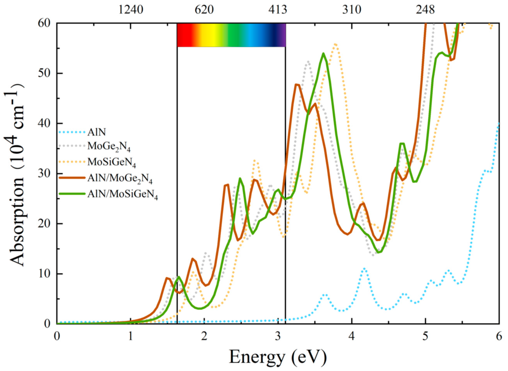
3. Results and Discussion

Firstly, the geometric and electronic structures of AlN, MoGe2N4, and MoSiGeN4 monolayers were studied. The construction of AlN, MoGe2N4, and MoSiGeN4 monolayers was based on previously reported experimental and calculated lattice parameters [52,53,54]. Figure 1a presents the top and side views of the geometric structure of the AlN monolayer, revealing its hexagonal structure. The band gap, calculated as 3.78 eV using the HSE06 method, aligns with the value of 2.93 eV obtained by the PBE method, consistent with existing literature [52]. For the MoGe2N4 monolayer depicted in Figure 1b, its geometric configuration is illustrated, with its original cell comprising 1 Mo, 2 Ge, and 4 N atoms. The MoGe2N4 monolayer is characterized as an indirect semiconductor with a band gap of 1.27 eV (PBE calculated value of 0.94 eV) [47]. Figure 1c,f display the geometric configuration and band structure of MoSiGeN4, with a band gap of 1.75 eV (PBE calculated value of 1.37 eV) [55]. Additionally, Figure 1d–f present the band diagrams obtained from HSE06 functional calculations for AlN, MoGe2N4, and MoSiGeN4 monolayers, showcasing their indirect band gaps of 3.78 eV, 1.27 eV, and 1.75 eV, respectively. These values are consistent with previous experimental and theoretical studies [43,56,57]. In summary, while some properties of these three monolayers exhibit potential for improvement, several stacked structures were constructed using quantum methods, with strain distributed between the MoGe2N4/AlN and MoSiGeN4/AlN layers.
As shown in Table 1, the fully relaxed bond lengths of AlN and MoGe2N4 monolayers were 1.78 Å for Al-N and 2.121 Å for Mo-N, respectively. Considering MoSiGeN4 as a Janus two-dimensional material, the bond lengths of Mo-N1 and Mo-N2 were 2.101 Å and 2.104 Å, respectively, consistent with previous research results [58,59]. Furthermore, the relaxed lattice constants of AlN, MoGe2N4, and MoSiGeN4 were estimated at 3.120 Å, 3.021 Å, and 2.956 Å, respectively [40,43,56].
The binding energy is one of the effective methods to evaluate the stability of heterostructures. Through this approach, we calculate the binding energy (Eb) of heterostructures using the following formula:
E b = E v d W E A l N E e i t h e r
Here, EvdW is the energy of the MoGe2N4/AlN or MoSiGeN4/AlN heterostructure, EAlN is the energy of the AlN monolayer, and Eeither is the energy of the MoGe2N4 or MoSiGeN4 monolayer. According to the equation, the negative Eb value indicates that the energy of the heterostructure is stable, with a more negative value suggesting greater stability. Therefore, the stacking method with a negative binding energy and relatively low interfacial adhesion energy was selected.
Given the similarity in lattice constants among these three monolayers, a lattice mismatch rate of less than 5% can be achieved without the establishment of a supercell. The chosen vdWs heterostructures consist of the AlN cell, MoGe2N4 cell, and MoSiGeN4 cell. Additionally, considering the differences in structural stacking, we investigated six high-symmetry stacking methods for research purposes. For these MoGe2N4/AlN (Figure 2a) and MoSiGeN4/AlN (Figure 2b) heterostructures, a comparative approach was employed, such as utilizing the same stacking method for AB1 and AC1. As two-dimensional materials extend infinitely on the plane, we examined the top view and side view of these six geometric structures, detailing each structure comprehensively. Under the convergence criterion, all structures underwent geometric optimization concerning energy and force. The results revealed that the MoGe2N4/AlN heterostructure exhibits a band gap ranging from 1.64 eV to 1.76 eV (Figure 3a). Notably, the fifth stacking mode (AB5) demonstrated a type-II heterostructure with a direct band gap of 0.89 eV. Under solar illumination, electrons in the VBM of the AlN or MoGe2N4 layer were excited and transitioned to their CBM, leaving behind holes in their VBM. Subsequently, driven by the built-in electric field between layers, electrons in the CBM of MoGe2N4 layer transferred and accumulated toward the CBM of the AlN layer. Similarly, holes accumulated in the VBM of the MoGe2N4 layer. Electrons and holes accumulated in different layers, effectively suppressing the recombination of photo-generated electrons and holes, enhancing its photocatalytic activity. On the other hand, the MoSiGeN4/AlN heterostructure displays an indirect band gap ranging from 1.26 eV to 1.42 eV (Figure 3b), smaller than the band gaps of 1.75 eV and 3.78 eV of the MoSiGeN4 and AlN monolayers, respectively. Due to the relatively small lattice mismatch rate of the heterostructure and the negative interface adhesion energy corresponding to the weak vdW bonding between the constituent layers, successful experimental preparation is feasible. The fifth stacking method was adopted for both the MoGe2N4/AlN and the MoSiGeN4/AlN heterostructures to study the impact of applied strain and electric field on their electronic structures.
To delve deeper into the electronic properties of the MoGe2N4/AlN and MoSiGeN4/AlN heterostructures, we generated three-dimensional charge density difference plots for these two heterostructures, as illustrated in Figure 4. The calculation formula is defined as follows:
Δ ρ = ρ v d W ρ A l N ρ e i t h e r
Here, ρ v d W and ρ A l N denote the total charge density of the heterostructure and the charge density of the AlN monolayer, respectively, and ρ e i t h e r  denotes the charge density of the MoGe2N4 or MoSiGeN4 monolayer. The resulting three-dimensional charge density difference is depicted in Figure 4, where the green region signifies charge depletion and the orange region signifies charge accumulation. As depicted in Figure 4, charge transfer is evident at the interfaces of the MoGe2N4/AlN and MoSiGeN4/AlN heterojunctions.
Furthermore, we conducted the Bader charge analysis of the heterostructure to quantify the charge transfer, as shown in Table 2. The results indicate that 0.0486 electrons were transferred from the MoGe2N4 layer to the AlN layer in the MoGe2N4/AlN heterostructure, while 0.0187 electrons were transferred from the MoSiGeN4 layer to the AlN layer in the MoSiGeN4/AlN heterostructure. This electron transfer led to the formation of a built-in electric field at the interface of the heterostructure.
Next, we proceeded by investigating the impact of biaxial strain on the electronic characteristics of the MoGe2N4/AlN and MoSiGeN4/AlN vdW heterostructures. Biaxial strains ranging from −5% to 5%, incremented by 1%, were applied to the heterostructures. Figure 5 illustrates the band gap profiles of the heterostructures under varying biaxial strains. It is evident that the electronic properties of the MoGe2N4/AlN heterostructures are sensitive to biaxial strain. With an increment in biaxial strain from 0 to 5%, the band gap of the heterostructure was found to exhibit a diminishing trend, transitioning from a type-II direct band gap to a type-I indirect band gap at a strain of 4%. Conversely, as the biaxial strain decreased incrementally, the band gap value displayed an increasing trend. The heterostructure maintained a type-II direct band gap as the strain diminished, leading to an augmentation in the band gap value. Similarly, the band gap behavior of the MoSiGeN4/AlN heterostructure was found to align with that of MoGe2N4/AlN, demonstrating a linearly decreasing trend with increasing biaxial strain. Conversely, as the biaxial strain decreased incrementally, the band gap value exhibited a linearly increasing trend. Notably, under a −4% biaxial strain, the heterostructure transitioned from a type-I indirect band gap to a type-II direct band gap. Additionally, it can be inferred from Figure 5 that when the direct band gap was of type-II, the valence band maximum (VBM) of both the MoGe2N4/AlN and the MoSiGeN4/AlN heterostructures was contributed to by AlN. Conversely, when it was a type-I indirect band gap, the VBM and conduction band minimum (CBM) of these two heterostructures originated from MoGe2N4 and MoSiGeN4, respectively.
To tailor the band gap of heterostructures to nanoelectronic devices, we explored the effect of an electric field on their electronic properties. The electric field applied to the heterostructures ranged from −0.3 V/Å to 0.3 V/Å, incremented by 0.1 V/Å. Figure 6 illustrates the band gap variation of the heterostructures under the influence of the electric field. The band gap of the MoGe2N4/AlN heterostructure was found to exhibit a linear increase in the range of −0.3 V/Å to 0.3 V/Å. Notably, the heterostructure transitioned from a type II direct band gap to a type-I indirect band gap at +0.1% V/Å. Conversely, the band gap value of the MoSiGeN4/AlN heterostructure initially increased and then decreased with the application of the electric field. Specifically, a change in the band gap type occurred when the electric field was set to −1% V/Å. In the range of −0.3% V/Å to −0.1% V/Å, the heterostructure demonstrated a type-II direct band gap. Remarkably, the band gap types of these two heterostructures can be modulated by the applied electric field, offering the possibility of adjusting both the MoGe2N4/AlN and the MoSiGeN4/AlN heterostructures. The band gap characteristics of the heterojunctions provide valuable theoretical insights for experimentalists to effectively engineer photocatalytic hydrogen production heterojunctions of two-dimensional materials and integrate them into optoelectronic devices.
Expanding beyond band gap considerations, the optical absorption spectra of AlN, MoGe2N4, and MoSiGeN4 monolayers, along with MoGe2N4/AlN and MoSiGeN4/AlN heterostructures, were analyzed as important indicators for photovoltaic device materials, as depicted in Figure 7. Different colors represent various two-dimensional materials. Dashed lines illustrate the optical absorption spectra of individual monolayers, while solid lines depict the optical absorption spectra of the constructed heterostructures. Notably, both the MoGe2N4/AlN and the MoSiGeN4/AlN heterostructures were found to exhibit significantly stronger absorption of the visible light compared to the single-layer AlN, MoGe2N4, and MoSiGeN4, effectively compensating for the deficiencies in visible light absorption of the AlN monolayer. Moreover, the peak absorption coefficients of these two heterostructures were both close to 30 × 105 cm−1. This enhancement also renders these heterostructures superior with respect to optical properties compared to certain other photovoltaic materials [60]. This heightened absorption capability suggests that these heterostructures possess enhanced potential for efficiently utilizing solar energy, rendering them promising candidates for photovoltaic applications. The observed optical characteristics provide valuable insights for experimentalists, facilitating the effective engineering of photocatalytic hydrogen production heterojunctions using two-dimensional materials and their integration into advanced optoelectronic devices.

4. Conclusions

In summary, we investigated the electronic properties of the MoGe2N4/AlN and MoSiGeN4/AlN van der Waals heterostructures through density functional theory simulations, examining their responses to biaxial strain and vertical electric fields. Our findings reveal that different stacking methods significantly impact the electronic properties of these heterostructures. While all six high-symmetry structures of the MoSiGeN4/AlN heterostructures exhibit type-I indirect band gaps, the situation differs for the MoGe2N4/AlN heterostructures, among which the AB5 configuration manifests a type-II direct band gap. Notably, for a given heterostructure, the band gap exhibits fluctuations within a certain range. Under the influence of biaxial strain and electric fields, the band gap type of the heterostructure undergoes effective transformation. Particularly, the band gap value of the MoSiGeN4/AlN heterostructure exhibits relatively significant changes under biaxial strain. In the presence of an electric field ranging from −0.3 V/Å to −0.1 V/Å, the MoSiGeN4/AlN heterostructures transition from a type-I indirect band gap to a type-II direct band gap. These findings underscore the potential for effectively adjusting the electronic properties of the MoGe2N4/AlN and MoSiGeN4/AlN heterostructures through strain and applied electric fields, enabling modifications of the band gap type. Such insights offer valuable theoretical guidance for the efficient preparation and utilization of these heterostructures, indicating promising applications in optoelectronic devices and photocatalysis.

Author Contributions

Conceptualization, B.X., Z.L. and L.X.; Methodology, J.S.; Validation, J.S., B.X., Z.J. and Q.W.; Formal analysis, Z.L., K.D. and L.X.; Investigation, J.Z.; Data curation, J.S.; Writing—original draft, J.S.; Writing—review & editing, J.Z., Q.W., K.D. and L.X.; Visualization, J.S., B.X. and L.X.; Supervision, B.X., Z.L., L.-L.W., K.D. and L.X.; Project administration, L.X.; Funding acquisition, L.X. All authors have read and agreed to the published version of the manuscript.

Funding

This work was financially supported by the National Nature Science Foundation of China (Grant No. 52263031), the Jiangxi Provincial Natural Science Foundation (Grant Nos. 20212BAB201013, 20202ACBL211004), and the Open Project Program of Jiangxi Provincial Key Laboratory for Simulation and Modelling of Particulate Systems, Jiangxi University of Science and Technology.

Institutional Review Board Statement

Not applicable.

Informed Consent Statement

Not applicable.

Data Availability Statement

Data are contained within the article.

Conflicts of Interest

The authors declare no conflict of interest.

References

  1. Kruitwagen, L.; Story, K.T.; Friedrich, J.; Byers, L.; Skillman, S.; Hepburn, C. A global inventory of photovoltaic solar energy generating units. Nature 2021, 598, 604–610. [Google Scholar] [CrossRef] [PubMed]
  2. Yang, Z.; Gao, R.; Hu, N.; Chai, J.; Cheng, Y.; Zhang, L. The Prospective Two-Dimensional Graphene Nanosheets: Preparation, Functionalization and Applications. Nano-Micro Lett. 2012, 4, 1–9. [Google Scholar] [CrossRef]
  3. Kumar, R.; Sahoo, S.; Joanni, E.; Singh, R.K.; Yadav, R.M.; Verma, R.K.; Singh, D.P.; Tan, W.K.; Pérez del Pino, A.; Moshkalev, S.A.; et al. A review on synthesis of graphene, h-BN and MoS2 for energy storage applications: Recent progress and perspectives. Nano Res. 2019, 12, 2655–2694. [Google Scholar] [CrossRef]
  4. Novoselov, K.S.; Geim, A.K.; Morozov, S.V.; Jiang, D.; Zhang, Y.; Dubonos, I.V.; Grigorieva, A.; Firsov, A. Electric field effect in atomically thin carbon films. Science 2004, 306, 666–669. [Google Scholar] [CrossRef] [PubMed]
  5. Geim, A.K.; Novoselov, K.S. The rise of graphene. Nat. Mater. 2007, 6, 183–191. [Google Scholar] [CrossRef] [PubMed]
  6. Zhang, C.; Ma, Y.; Zhang, X.; Abdolhosseinzadeh, S.; Sheng, H.; Lan, W.; Pakdel, A.; Heier, J.; Nüesch, F. Two-Dimensional Transition Metal Carbides and Nitrides (MXenes): Synthesis, Properties, and Electrochemical Energy Storage Applications. Energy Environ. Mater. 2020, 3, 29–55. [Google Scholar] [CrossRef]
  7. Khan, K.; Tareen, A.K.; Aslam, M.; Wang, R.; Zhang, Y.; Mahmood, A.; Ouyang, Z.; Zhang, H.; Guo, Z. Recent developments in emerging two-dimensional materials and their applications. J. Mater. Chem. C 2020, 8, 387–440. [Google Scholar] [CrossRef]
  8. Liu, Y.; Weiss, N.O.; Duan, X.; Cheng, H.C.; Huang, Y.; Duan, X. Van der Waals heterostructures and devices. Nat. Rev. Mater. 2016, 1, 16042. [Google Scholar] [CrossRef]
  9. Tho, C.C.; Guo, S.D.; Liang, S.J.; Ong, W.L.; Lau, C.S.; Cao, L.; Wang, G.; Ang, Y.S. MA2Z4 family heterostructures: Promises and prospects. Appl. Phys. Rev. 2023, 10, 041307. [Google Scholar] [CrossRef]
  10. Wang, S.; Ren, C.; Tian, H.; Yu, J.; Sun, M. MoS2/ZnO van der Waals heterostructure as a high-efficiency water splitting photocatalyst: A first-principles study. J. Phys. Chem. Chem. Phys. 2018, 20, 13394–13399. [Google Scholar] [CrossRef]
  11. Meng, X.; Shen, Y.; Liu, J.; Lv, L.; Yang, X.; Gao, X.; Zhou, M.; Wang, X.; Zheng, Y.; Zhou, Z. The PtSe2/GaN van der Waals heterostructure photocatalyst with type-II alignment: A first-principles study. J. Appl. Catal. A 2021, 624, 118332. [Google Scholar] [CrossRef]
  12. Liang, S.J.; Cheng, B.; Cui, X.; Miao, F. Van der Waals heterostructures for high-performance device applications: Challenges and opportunities. J. Adv. Mater. 2020, 32, 1903800. [Google Scholar] [CrossRef] [PubMed]
  13. Geim, A.K.; Grigorieva, I.V. Van der waals heterostructures. Nature 2013, 499, 419. [Google Scholar] [CrossRef]
  14. Xin, K.; Wang, X.; Grove-Rasmussen, K.; Wei, Z. Twist-angle two-dimensional superlattices and their application in (opto) electronics. J. Semicond. 2022, 43, 011001. [Google Scholar] [CrossRef]
  15. Pham, P.V.; Bodepudi, S.C.; Shehzad, K.Y.; Liu, Y.; Xu, Y.; Yu, B.; Duan, X. 2D heterostructures for ubiquitous electronics and optoelectronics: Principles, opportunities, and challenges. Chem. Rev. 2022, 122, 6514. [Google Scholar] [CrossRef] [PubMed]
  16. Castellanos-Gomez, A.; Buscema, M.; Molenaar, R.; Singh, V.; Janssen, L.; van der Zant, H.S.J.; Steele, G.A. Deterministic transfer of two-dimensional materials by all-dry viscoelastic stamping. 2D Mater. 2014, 1, 011002. [Google Scholar] [CrossRef]
  17. Gurarslan, A.; Yu, Y.; Su, L.; Suarez, F.; Yao, S.; Zhu, Y.; Ozturk, M.; Zhang, Y.; Cao, L. Surface-energy-assisted perfect transfer of centimeter-scale monolayer and few-layer MoS2 films onto arbitrary substrates. ACS Nano 2014, 8, 11522–11528. [Google Scholar] [CrossRef]
  18. Cui, X.; Kong, Z.; Gao, E.; Huang, D.; Hao, Y.; Shen, H.; Di, C.A.; Xu, Z.; Zheng, J.; Zhu, D. Rolling up transition metal dichalcogenide nanoscrolls via one drop of ethanol. Nat. Commun. 2018, 9, 1301. [Google Scholar] [CrossRef]
  19. Zaretski, A.V.; Moetazedi, H.; Kong, C.; Sawyer, E.J.; Savagatrup, S.; Valle, E.; O’Connor, T.F.; Printz, A.D.; Lipomi, D.J. Metal-assisted exfoliation (MAE): Green, roll-to-roll compatible method for transferring graphene to flexible substrates. Nanotechnology 2015, 26, 045301. [Google Scholar] [CrossRef] [PubMed]
  20. Bae, S.H.; Zhou, X.; Kim, S.; Lee, Y.S.; Cruz, S.S.; Kim, Y.; Hannon, J.B.; Yang, Y.; Sadana, D.K.; Ross, F.M.; et al. Unveiling the carrier transport mechanism in epitaxial graphene for forming wafer-scale, single-domain graphene. Proc. Natl. Acad. Sci. USA 2017, 114, 4082. [Google Scholar] [CrossRef]
  21. Zeng, J.; Xu, L.; Yang, Y.; Luo, X.; Li, H.J.; Xiong, S.; Wang, L.L. Boosting the photocatalytic hydrogen evolution performance of monolayer C2N coupled with MoSi2N4: Density-functional theory calculations. Phys. Chem. Chem. Phys. 2021, 23, 8318. [Google Scholar] [CrossRef] [PubMed]
  22. Hussain, G.; Asghar, M.; Iqbal, M.W.; Ullah, H.; Autieri, C. Exploring the structural stability, electronic and thermal attributes of synthetic 2d materials and their heterostructures. Appl. Surf. Sci. 2022, 590, 153131. [Google Scholar] [CrossRef]
  23. Ren, Y.T.; Hu, L.; Chen, Y.T.; Hu, Y.J.; Wang, J.L.; Gong, P.L.; Zhang, H.; Huang, L.; Shi, X.Q. Two-dimensional MSi2N4 monolayers and van der waals heterostructures: Promising spintronic properties and band alignments. Phys. Rev. Mater. 2022, 6, 064006. [Google Scholar] [CrossRef]
  24. Wang, G.; Chang, J.; Tang, W.; Xie, W.; Ang, Y.S. 2D materials and heterostructures for photocatalytic water-splitting: A theoretical perspective. J. Phys. D 2022, 55, 293002. [Google Scholar] [CrossRef]
  25. Wang, H.; Zhang, L.; Chen, Z.; Hu, J.; Li, S.; Wang, Z.; Liu, J.; Wang, X. Semiconductor heterojunction photocatalysts:design, construction, and photocatalytic performances. Chem. Soc. Rev 2014, 43, 5234–5244. [Google Scholar] [CrossRef] [PubMed]
  26. Wang, W.; Zheng, Y.; Li, X.; Li, Y.; Zhao, H.; Huang, L.; Yang, Z.; Zhang, X.; Li, G. 2D AlN layers sandwiched between graphene and Si substrates. Adv. Mater. 2019, 31, 1803448. [Google Scholar] [CrossRef] [PubMed]
  27. Wang, G.; Dang, S.; Zhang, P.; Xiao, S.; Wang, C.; Zhong, M. Hybrid density functional study on the photocatalytic properties of AlN/MoSe2, AlN/WS2, and AlN/WSe2 heterostructures. J. Phys. D Appl. Phys. 2018, 51, 025109. [Google Scholar] [CrossRef]
  28. Yu, R.; Liu, G.; Wang, G.; Chen, C.; Xu, M.; Zhou, H. Ultrawide-bandgap semiconductor AlN crystals: Growth and applications. J. Mater. 2021, 9, 1852–1873. [Google Scholar] [CrossRef]
  29. Wang, Z.; Wang, G.; Liu, X.; Wang, S.; Wang, T.; Zhang, S.; Zhang, L. Two-dimensional wide band-gap nitride semiconductor GaN and AlN materials: Properties, fabrication and applications. J. Mater. 2021, 9, 17201–17232. [Google Scholar] [CrossRef]
  30. Hong, Y.L.; Liu, Z.B.; Wang, L.; Zhou, T.Y.; Ma, W.; Xu, C.; Feng, S.; Chen, L.; Chen, M.L.; Sun, D.M.; et al. Chemical vapor deposition of layered two-dimensional MoSi2N4 Materials. Science 2020, 369, 670–674. [Google Scholar] [CrossRef]
  31. Zhang, R.; Zhang, Y.; Wei, X.; Guo, T.; Fan, J.; Ni, L.; Weng, Y.; Zha, Z.; Liu, J.; Tian, Y.; et al. Type-II band alignment AlN/InSe van der Waals heterostructure: Vertical strain and external electric field. Appl. Surf. Sci. 2020, 528, 146782. [Google Scholar] [CrossRef]
  32. Novoselov, K.S. Discovery of 2D van der Waals layered MoSi2N4 family. Natl. Sci. Rev. 2020, 7, 1842–1844. [Google Scholar] [CrossRef] [PubMed]
  33. Pham, D.K. Electronic properties of a two-dimensional van der waals MoGe2N4/MoSi2N4 heterobilayer: Effect of the insertion of a graphene layer and interlayer coupling. RSC Adv. 2021, 11, 28659–28666. [Google Scholar] [CrossRef] [PubMed]
  34. Guo, Y.; Min, J.; Cai, X.; Zhang, L.; Liu, C.; Jia, Y. Two-dimensional type-II BP/MoSi2P4 vdw heterostructures for high-performance solar cells. J. Phys. Chem. C 2022, 126, 4677. [Google Scholar] [CrossRef]
  35. Liu, C.; Wang, Z.; Xiong, W.; Zhong, H.; Yuan, S. Effect of vertical strain and in-plane biaxial strain on type-ii MoSi2N4/Cs3Bi2I9 van der waals heterostructure. J. Appl. Phys. 2022, 131, 163102. [Google Scholar] [CrossRef]
  36. Xu, L.; Zhang, Y.; Ma, Z.; Chen, T.; Guo, C.; Wu, C.; Li, H.; Huang, X.; Tang, S.; Wang, L.L. Indirect Z-scheme hydrogen production photocatalyst based on two-dimensional GeC/MoSi2N4 van der Waals heterostructures. Int. J. Hydrogen Energy 2023, 48, 18301–18314. [Google Scholar] [CrossRef]
  37. Li, X.; Li, Z.; Yang, J. Proposed photosynthesis method for producing hydrogen from dissociated water molecules using incident near-infrared light. Phys. Rev. Lett. 2014, 112, 018301. [Google Scholar] [CrossRef] [PubMed]
  38. Fu, C.F.; Sun, J.; Luo, Q.; Li, X.; Hu, W.; Yang, J. Intrinsic electric fields in two-dimensional materials boost the solar-to-hydrogen efficiency for photocatalytic water splitting. Nano. Lett. 2018, 18, 6312. [Google Scholar] [CrossRef]
  39. Yu, Y.; Zhou, J.; Guo, Z.; Sun, Z. Novel two-dimensional janus MoSiGeN4 and WSiGeN4 as highly efficient photocatalysts for spontaneous overall water splitting. ACS Appl. Mater. Interfaces 2021, 13, 28090. [Google Scholar] [CrossRef]
  40. Binh, N.T.; Nguyen, C.Q.; Vu, T.V.; Nguyen, C.V. Interfacial Electronic Properties and Tunable Contact Types in Graphene/Janus MoGeSiN4 Heterostructures. J. Phys. Chem. Lett. 2021, 12, 3934–3940. [Google Scholar] [CrossRef]
  41. Lv, X.; Huang, H.; Mao, B.; Liu, G.; Zhao, G.; Yang, J. Dipole-regulated bandgap and high electron mobility for bilayer janus MoSiGeN4. Appl. Phys. Lett. 2022, 120, 21. [Google Scholar] [CrossRef]
  42. Wang, J.; Zhao, X.; Hu, G.; Ren, J.; Yuan, X. Manip-ulable electronic and optical properties of two-dimensional MoSTe/MoGe2N4 van der waals heterostructures. Nanomaterials 2021, 11, 3338. [Google Scholar] [CrossRef] [PubMed]
  43. Mortazavi, B.; Javvaji, B.; Shojaei, F.; Rabczuk, T.; Shapeev, A.V.; Zhuang, X. Exceptional piezoelectricity, high thermal conductivity and stiffness and promising photocatalysis in two-dimensional MoSi2N4 family confirmed by first-principles. Nano Energy 2021, 82, 105716. [Google Scholar] [CrossRef]
  44. Kresse, G.; Furthmüller, J. Efficiency of ab-initio total energy calculations for metals and semiconductors using a plane-wave basis set. Comput. Mater. Sci. 1996, 6, 15–50. [Google Scholar] [CrossRef]
  45. Kresse, G.; Furthmüller, J. Efficient iterative schemes for ab initio total-energy calculations using a plane-wave basis set. Phys. Rev. B 1996, 54, 11169. [Google Scholar] [CrossRef] [PubMed]
  46. Kresse, G.; Joubert, D. From ultrasoft pseudopotentials to the projector augmented-wave method. Phys. Rev. B 1999, 59, 1758. [Google Scholar] [CrossRef]
  47. Perdew, J.P.; Burke, K.; Ernzerhof, M. Generalized gradient approximation made simple. Phys. Rev. Lett. 1996, 77, 3865. [Google Scholar] [CrossRef]
  48. Grimme, S.; Antony, J.; Ehrlich, S.; Krieg, H. A consistent and accurate ab initio parametrization of density functional dispersion correction (DFT-D) for the 94 elements H-Pu. J. Chem. Phys. 2010, 132, 15. [Google Scholar] [CrossRef]
  49. Heyd, J.; Scuseria, G.E.; Ernzerhof, M. Hybrid functionals based on a screened coulomb potential. J. Chem. Phys. 2003, 118, 8207–8215. [Google Scholar] [CrossRef]
  50. Grimme, S. Semiempirical Gga-type density functional constructed with a long-range dispersion correction. J. Comput. Chem. 2006, 27, 1787–1799. [Google Scholar] [CrossRef]
  51. Momma, K.; Izumi, F. VESTA: A three-dimensional visualization system for electronic and structural analysis. J. Appl. Crystallogr. 2008, 41, 653–658. [Google Scholar] [CrossRef]
  52. Tao, J.; Xu, L.; Li, C.; Xiong, S.; Xu, Z.; Shao, J.; Cao, L.; Zhang, Y.; Dong, K.; Wang, L.L. Two-dimensional AlN/TMO van der Waals heterojunction as a promising photocatalyst for water splitting driven by visible light. Phys. Chem. Chem. Phys. 2023, 25, 30924–30933. [Google Scholar] [CrossRef] [PubMed]
  53. Nguyen, C.; Hoang, N.V.; Phuc, H.V.; Sin, A.Y.; Nguyen, C.V. Two-dimensional boron phosphide/MoGe2N4 van der Waals heterostructure: A promising tunable optoelectronic material. J. Phys. Chem. Lett. 2021, 12, 5076–5084. [Google Scholar] [CrossRef] [PubMed]
  54. Guo, S.D.; Mu, W.Q.; Zhu, Y.T.; Han, R.Y.; Ren, W.C. Predicted septuple-atomic-layer Janus MSiGeN4 (M = Mo and W) monolayers with Rashba spin splitting and high electron carrier mobilities. J. Mater. Chem. 2021, 9, 2464–2473. [Google Scholar] [CrossRef]
  55. Li, X.; Li, T.; Wang, J.; Song, X. Adsorption behavior of Janus MoSiGeN4 monolayer for gas-sensing application with high sensitivity and reuse. Phys. E 2023, 153, 115777. [Google Scholar] [CrossRef]
  56. Zou, H.; Peng, M.; Zhou, W.; Pan, J.; Ouyang, F. Type II GaS/AlN van der Waals heterostructure: Vertical strain, in-plane biaxial strain and electric field effect. Phys. E Low-Dimens. Syst. Nanostructures 2021, 126, 114481. [Google Scholar] [CrossRef]
  57. Huang, X.; Xu, L.; Xiao, B.; Dong, K.; Yang, K.; Li, L. High-efficiency photocatalyst based on a MoSiGeN4/SiC heterojunction. J. Mater. Sci. 2022, 57, 16404. [Google Scholar] [CrossRef]
  58. Queen, J.D.; Irvankoski, S.; Fettinger, J.C.; Tuononen, H.M.; Power, P.P. A monomeric aluminum imide (iminoalane) with Al–N triple-bonding: Bonding analysis and dispersion energy stabilization. J. Am. Chem. Soc. 2021, 143, 6351–6356. [Google Scholar] [CrossRef] [PubMed]
  59. Zeng, J.; Xu, L.; Luo, X.; Chen, T.; Tang, S.; Huang, X.; Wang, L.L. Z-scheme systems of ASi2N4 (A = Mo or W) for photocatalytic water splitting and nanogenerators. Tungsten 2022, 4, 52–59. [Google Scholar] [CrossRef]
  60. Yin, Y.; Gong, Q.; Yi, M.; Guo, W. Emerging Versatile Two-Dimensional MoSi2N4 Family. J. Adv. Funct. Mater. 2023, 33, 2214050. [Google Scholar] [CrossRef]
Figure 1. The geometric structure of (a) AlN, (b) MoGe2N4, and (c) MoSiGeN4 monolayers. The calculated band structure and its DOS and PDOS of (d) AlN, (e) MoGe2N4, and (f) MoSiGeN4 monolayers. The Fermi level was set to zero.
Coatings 14 00500 g001
Figure 2. Top and side views of optimized (a) AB1, AB2, AB3 AB4, AB5, and AB6 different stacking modes of MoGe2N4/AlN; (b) AC1, AC2, AC3, AC4, AC5, and AC6 different stacking modes of MoSiGeN4/AlN.
Coatings 14 00500 g002
Figure 3. The band structure of six different stacking heterostructures relative to (a) MoGe2N4/AlN and (b) MoSiGeN4/AlN. The Fermi level was set to zero.
Coatings 14 00500 g003
Figure 4. The 3D charge density difference of heterostructures (a) MoGe2N4/AlN and (b) MoSiGeN4/AlN. The orange and green regions represent charge accumulation and consumption, respectively.
Coatings 14 00500 g004
Figure 5. The band gap plots of (a) AlN/MoGe2N4 and (b) AlN/MoSiGeN4 as a function of the strain.
Coatings 14 00500 g005
Figure 6. The band structure of (a) MoGe2N4/AlN and (b) MoSiGeN4/AlN under the action of an external electric field, with corresponding external electric field values at the bottom. The Fermi level was set to zero.
Coatings 14 00500 g006
Figure 7. The optical absorption spectra of isolated monolayers and heterostructure. The ribbon area represents the visible light absorption range.
Coatings 14 00500 g007
Table 1. The optimized lattice constant a (Å), interlayer distance d (Å), interlayer binding energy Eb (eV), and band gap with HSE06 function, EHSE06 (eV).
Structurea (Å)d (Å)Eb (eV)EHSE06 (eV)
AlN3.120--3.783
MoGe2N43.021--1.273
MoSiGeN42.956--1.753
AB5 (MoGe2N4/AlN)3.0062.852−0.0161.382
AC5 (MoSiGeN4/AlN)3.0552.637−0.1960.886
Table 2. The Bader charge analysis of AB5(MoGe2N4/AlN) and AC5(MoSiGeN4/AlN) vdW heterostructures. The gain and loss electrons are represented by negative and positive values, respectively.
StructureAB5(MoGe2N4/AlN)AC5(MoSiGeN4/AlN)
charge (e)AlN−0.0486Al−2.3120AlN−0.0187Al−2.3095
N+2.2634 N+2.2908
MoGe2N4+0.0486Mo−1.5126MoSiGeN4+0.0187Mo−1.5062
Ge−1.8670 Si−2.9019
N+1.3238Ge−1.8054
N+1.5580
Disclaimer/Publisher’s Note: The statements, opinions and data contained in all publications are solely those of the individual author(s) and contributor(s) and not of MDPI and/or the editor(s). MDPI and/or the editor(s) disclaim responsibility for any injury to people or property resulting from any ideas, methods, instructions or products referred to in the content.

