
Plasma Bombardment-Induced Amorphization of (TiNbZrCr)Nx High-Entropy Alloy Nitride Films
by
 ,
,
Yantao Li
1,
Donglin Ma
2,*,
Jun Liang
1,
Deming Huang
1,
Libo Wang
1,
Diqi Ren
2,
Xin Jiang
3 and
Yongxiang Leng
3,4 1
School of Mechanical and Electrical Engineering, Mianyang Teachers’ College, Mianyang 621000, China
2
College of Physics and Engineering, Chengdu Normal University, Chengdu 611130, China
3
Key Laboratory of Advanced Technologies of Materials, Ministry of Education, School of Materials Science and Engineering, Southwest Jiaotong University, Chengdu 610031, China
4
Sichuan Province International Science and Technology Cooperation Base of Functional Materials, College of Medicine, Southwest Jiaotong University, Chengdu 610031, China
*
Author to whom correspondence should be addressed.
Coatings 2024, 14(4), 505; https://doi.org/10.3390/coatings14040505
Submission received: 23 March 2024
/
Revised: 14 April 2024
/
Accepted: 16 April 2024
/
Published: 19 April 2024
(This article belongs to the Collection Strong, Ductile and Corrosion-Resistant High-Entropy Alloys)
Abstract
:The (TiNbZrCr)Nx high-entropy nitride films (HENFs) were prepared by high-power pulsed magnetron sputtering (HPPMS). The effect of the N2 flow rate (FN) on the HPPMS plasma discharge, film composition, microstructure, residual stress, tribological properties, and corrosion resistance was investigated. Results show that, with the increase in FN, plasma discharge is enhanced. Firstly, the introduced N atoms react with Ti, Nb, Cr, and Zr to form an FCC nitride phase structure. Then, with the increase in plasma bombardment on the deposited film, the HENFs undergo amorphization to form an FCC+ amorphous structure, accompanied by a decrease in grain size and a change in the preferred orientation from (1 1 1) to (2 0 0). The HENFs deposited at FN = 8 sccm show the highest hardness of 27.8 GPa. The HENFs deposited at FN = 12 sccm present the best tribological properties, with a low wear rate of 4.0 × 10⁻⁶ mm3N−1m−1. The corrosion resistance of the (TiNbZrCr)Nx HENFs shows a strong correlation with the amorphous phase. The corrosion resistance of the FCC nitride film is the worst, and the corrosion resistance gradually increases with the amorphous transformation of the film. Based on the above results, nanocomposite high-entropy films can be prepared using HPPMS technology and exhibit excellent, comprehensive performance.
1. Introduction
High-entropy alloy films [1] (HEFs) are a branch of high-entropy alloy materials consisting of four or more metals, each ranging from 5 to 35 at.%. And it inherits the characteristics of bulk high-entropy alloy materials, generally presenting single-phase FCC, BCC, or amorphous structures, exhibiting excellent properties such as high hardness [2,3,4], wear resistance [5,6,7], oxidation resistance [8], radiation resistance [9,10], and corrosion resistance [11,12]. Due to the high-entropy effect of the HEFs, the films are mostly single-phase solid solutions or amorphous structures.
Researchers are committed to preparing nanocomposite high-entropy films with biphasic or multiphase through energy and composition regulation methods to further improve the performance of high-entropy thin films. Liu et al. [13] fabricated ZrNbTiMo high-entropy alloy coatings using magnetron sputtering by changing the sputtering power and found that the films were a nanocomposite structure with amorphous encapsulated BCC structure nanocrystals, exhibiting excellent toughness and wear resistance. The author thought that the generation of nanocomposite structures was attributed to the sputtered atoms energy. When the energy of sputtered atoms was low, atom diffusion was inhibited, and the crystallization performance of the film decreased, ultimately leading to the coexistence of a large number of nanocrystals and amorphous areas. Braeckman et al. [14] prepared Nbx-CoCrCuFeNi high-entropy alloy films and found that with the introduction of Nb elements with large atomic radii, the film transformed from an FCC structure to an amorphous + FCC structure. The generation of such nanocomposite structures was related to the lattice strain generated by the introduction of Nb atoms with large atomic radius. If the Nb concentration became too high, the FCC lattice could not accommodate the atomic-level strains, and the amorphous configuration became more favorable. Yu et al. [15] prepared (AlCrTiZrMo)-Six-N high-entropy alloy nitride films by reactive magnetron sputtering and found that with the introduction of Si, a composite structure of the FCC nanocrystals and amorphous was formed in the film. The formation of FCC structure is related to the strong ordering ability of N atoms. Many reports have shown that the N atoms will react with elements such as Ti, Ta, Hf, Al, Ti, Zr, Mo, V, Nb, and Cr to form an FCC structure with multiple elements, while films without N are mostly amorphous. The incompatibility between amorphous SiN and the FCC (AlCrTiZrMo)N phase caused SiN to precipitate at the interface, resulting in a composite structure of amorphous SiN and nanocrystalline (AlCrTiZrMo)N [15]. Similar to the above, the precipitation of copper-rich phases can also form nanocomposite structures [16]. The above reports show that the formation of nanocomposite structures can be achieved by controlling the crystallization performance through energy, atomic size differences, or the chemical repulsion of atoms.
High-power pulsed magnetron sputtering (HPPMS) is a technology that applies high energy in the form of low-frequency pulses to the target to obtain high plasma density and a high sputtering particle ionization rate. The high ionization rate makes it easy to control the energy of sputtered particles and thus regulate the phase composition and microstructure of the films. In this paper, a new type of (TiNbZrCr)N high-entropy thin films (HENFs) was designed. The large atomic radius difference between Ti(1.45 Å), Nb(1.48 Å), Zr(1.60 Å), and Cr(1.27 Å) makes the film have a great tendency for amorphization. Moreover, they are all nitride-forming elements that easily combine with N to form a single-phase FCC structure. The N2 flow rate, known as an important factor affecting film properties, was tuned to study the corresponding influence on plasma discharge, composition, morphology, microstructure, hardness, tribological properties, and corrosion resistance.
2. Materials and Experimental Methods
The (TiNbZrCr)Nx HENFs were prepared onto polished stainless steel (316) and silicon wafers (Si) by HPPMS using an unbalanced magnetron sputtering equipment. The target is periodically spliced Ti (99.9%, 135 × 9 × 6 mm3), Nb (99.9%, 135 × 9 × 6 mm3), Cr (99.9%, 135 × 6 × 6 mm3), and Zr (99.9%, 135 × 6 × 6 mm3). And the target size is 135 × 170 × 6 mm3. After the base pressure of the chamber was pumped to 2 × 10⁻³ Pa, the Ar (99.999% in purity) was inlet as a working gas. The target and substrate were cleaned by Ar+ for 10 min and 20 min, respectively. Then a high-power pulsed magnetron sputtering source (HPS-450D, Chengdu Pulse Tech, Chengdu, China) was applied to the target. A 200 nm TiNbZrCr transition layer was prepared to improve the adhesion of the film, and then N2 (99.999% in purity) was introduced into the chamber to prepare a nitride film. The N2 flow rate was set as 0, 4, 8, 12, and 16 sccm. The detailed deposition parameters are shown in Table 1.
During the deposition, the plasma discharge current and voltage were monitored by an oscilloscope (TDS-220, Tektronix, Beaverton, OR, USA). The surface and cross-section morphologies of the HENFs were observed using field emission scanning electron microscopy (SEM, JSM-7800F, JEOL, Tokyo, Japan) with an acceleration voltage of 5 kV. The coating composition was measured by the energy dispersive spectroscopy (EDS, Oxford, UK) attached to the scanning electron microscope (SEM, JSM-7800F, Japan), and the acceleration voltage during testing was 15 kV. The crystalline structure of the HENFs was characterized by X-ray diffraction (XRD, Empyrean, Dordrecht, The Netherlands) with Cu kα radiation. The average grain size of the HENFs was calculated from the full-width at half-maximum (FWHM) by Scherrer’s equation, and the FWHM was obtained from peak fitting of XRD patterns. To further study the crystal structure of films, the HENFs deposited at 12 sccm were investigated by transmission electron microscopy (TEM, JEM-2100F, Japan). The TEM sample was a flat sample prepared by ion thinning. The residual stress of the HENFs was measured by the wafer curvature method. The bending profile of the films was measured by a stylus profiler (XP-2, XP Metal Detectors, West Chester, PA, USA), and the residual stress of the films was calculated by a modified Stoney equation. The hardness of the HENFs was measured using a Vickers-shaped diamond indenter with a maximum load of 30 mN. The hardness of HENFs was measured by a nanoindentation tester (Nano Indenter@G200, Agilent, Santa Clara, CA, USA) using continuous stiffness mode (CSM) with a maximum indentation depth of 1000 nm. The tribological properties of the HENFs were tested by a tribometer (CSEM, Neuchâtel, Switzerland) with WC balls of diameter 6 mm as friction pairs at a load of 2 N in air. The wear is reciprocating, with a stroke of 6 mm and a set wear cycle of 3000 r (wear distance = 3000 × 2 × 6 mm). The morphologies of the wear tracks were observed by a field emission scanning electron microscope (SEM, JSM-7800F, Japan). The wear track profiles of the films were measured by a stylus profiler (XP-2, USA). Then the wear rate of the films was calculated by μ = V/LS, where μ, V, L, and S represent the wear rate, wear volume, load, and sliding distance, respectively. The corrosion resistance of the (TiNbZrCr)Nx films was determined by electrochemical polarization and electrochemical impedance spectroscopy (EIS) using an electrochemistry workstation (VersaSTAT 3F, Oak Ridge, TN, USA) in a 3.5 wt.% NaCl solution. A standard saturated calomel electrode (SCE) was used as a reference electrode, platinum was used as the counter electrode, and film was used as a working electrode. The frequency range was 0.01 to 100,000 Hz in the electrochemical impedance spectroscopy test, and the amplitude was 20 mV.
3. Results and Discussion
3.1. HPPMS Plasma Discharge and Composition
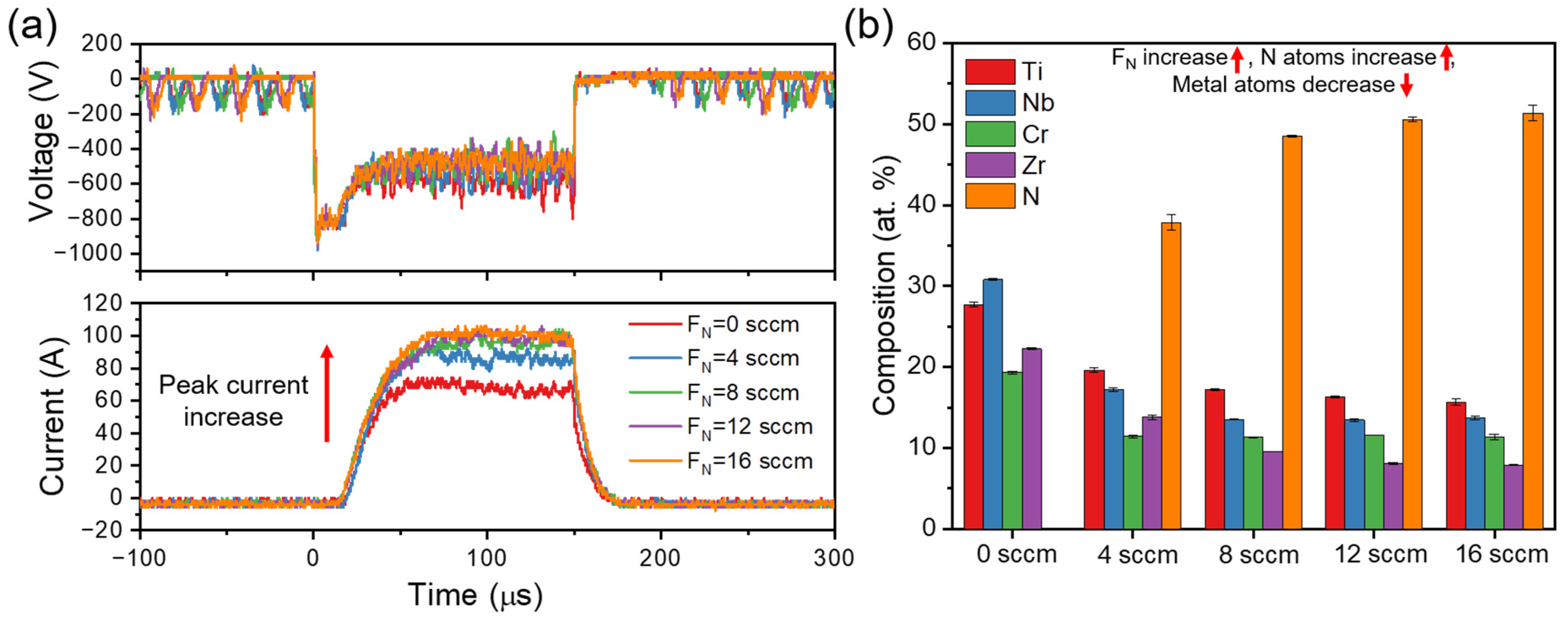
Figure 1a presents the discharge voltage and current waveforms at different FN. The target voltage is fixed at −800 V at different FN. The peak current is 72 A at FN = 0 sccm. With the introduction of N2 into the vacuum chamber, the peak current gradually increases and reaches 101 A at FN = 16 sccm. The increase in target current is closely related to the number of ions reaching the target and the number of electrons released from the target. The increase in N2 flow rate increases the deposition pressure and reduces the mean free path of atom movement, which results in more violent collisions of atoms on the target surface with electrons, and finally, a large number of ions are generated. In addition, compared with Ar, N is more likely to lose electrons and become N+ due to its lower ionization energy [17]. These ions reach the target surface and increase the target current. Also, the increased N ions will enhance the bombardment effect on the substrate, thereby affecting the growth of the thin film [18]. The secondary electrons emitted from the target are another factor that cannot be ignored [19]. Due to the target poisoning effect, a nitride layer will be produced on the surface of the target [20]. The secondary electron emission yield is higher for a nitride layer than a metal target, which will also lead to an increase in target current.
Figure 1b shows the composition of the (TiNbZrCr)Nx films prepared at different FN. The content of Ti, Nb, Cr, and Zr is in the range of 15.6%~27.7%, 13.7%~30.8%, 11.3%~19.3%, and 7.9%~22.2%, respectively, which meets the design criteria of high-entropy films. In addition, with the increase in FN, the N content in the HENFs gradually increases to the highest value of 51.4% at FN = 16 sccm, and the proportion of metal atoms gradually decreases.
3.2. Microstructure of the (TiNbZrCr)Nx HENFs
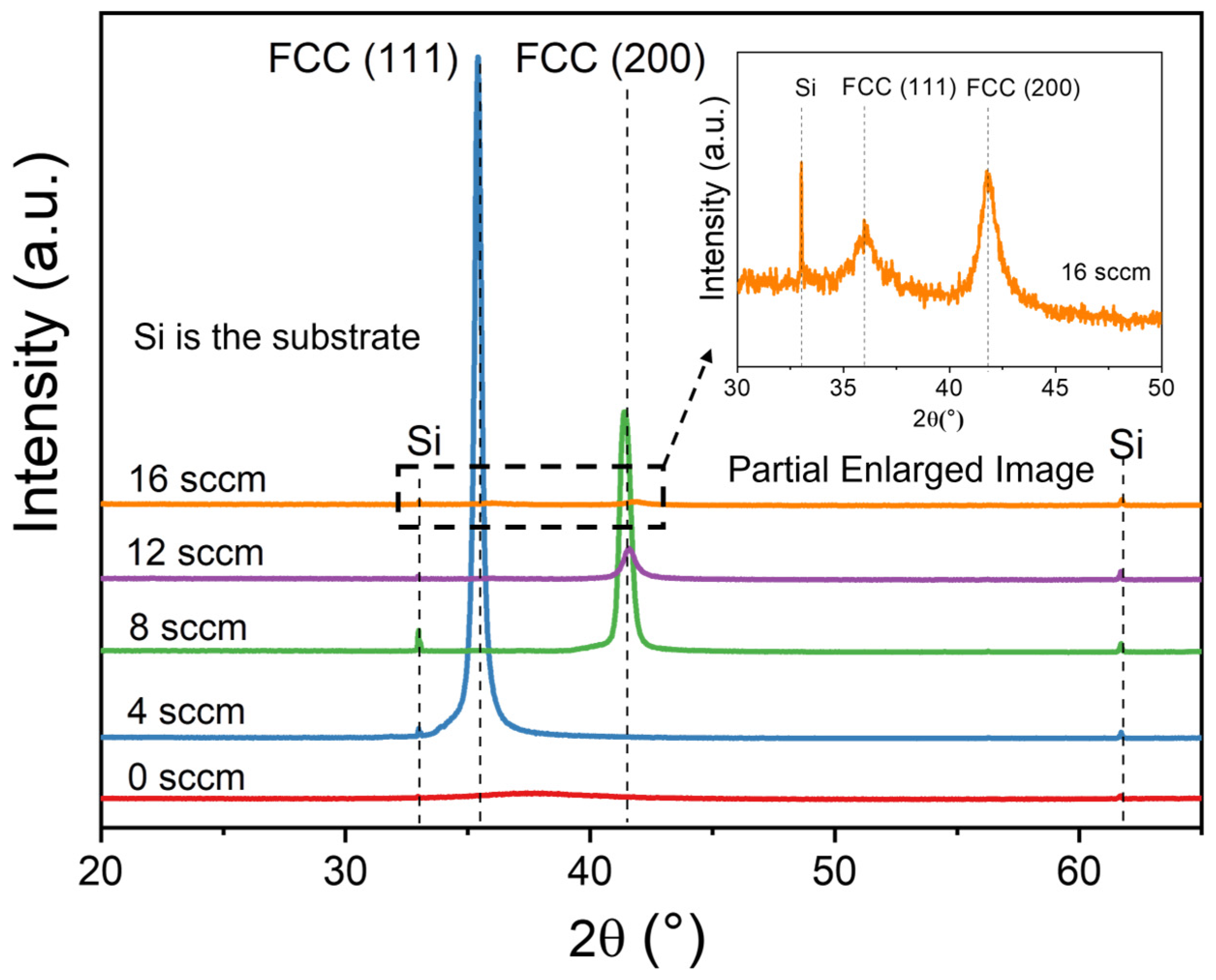
Figure 2 shows the XRD patterns of the (TiNbZrCr)Nx HENFs deposited under different FN. The appearance of Si diffraction peaks is the cause of the Si substrate. The HENFs deposited at FN = 0 sccm show a broad amorphous peak. With the introduction of nitrogen, a set of diffraction peaks of FCC appeared in the film, indicating a structural transformation of the film and the generation of a new FCC structure. A large number of studies [21,22,23] have reported that the introduction of N atoms into refractory high-entropy alloy will form the FCC structure ceramic phase. With the FN increasing from 4 sccm to 8 and 12 sccm, the FCC (2 0 0) peak dramatically increases and dominates. For the FCC nitride films, the preferred orientation of crystal planes depends on the competition between surface energy and strain energy. In an FCC structure, the (1 1 1) plane shows the lowest surface energy, while the (2 0 0) plane has the lowest strain energy. It is speculated that more energetic particles will be generated as FN increases, and these particles will bombard the growing film to inhibit the growth of film grains and promote the growth of low-strain energy crystal planes. Therefore, the grain size of the thin film gradually decreases, and the low strain energy (2 0 0) crystal plane dominates the film. In addition, with the increase in FN, the intensity of XRD diffraction peaks significantly decreases, and the peak width increases, indicating a decrease in the crystallinity of the thin film. The grain sizes of the films deposited at FN = 4, 8, 12, and 16 sccm are calculated by the Scherrer equation, which are 26.0, 18.0, 14.5, and 7.5 nm, respectively (Table 2). The decrease in grain size may be related to the enhanced bombardment effect. The bombardment effect can generate more defects, and the nucleation energy of the crystal decreases at the defect location, which gives the crystal nucleation an advantage over growth [3].
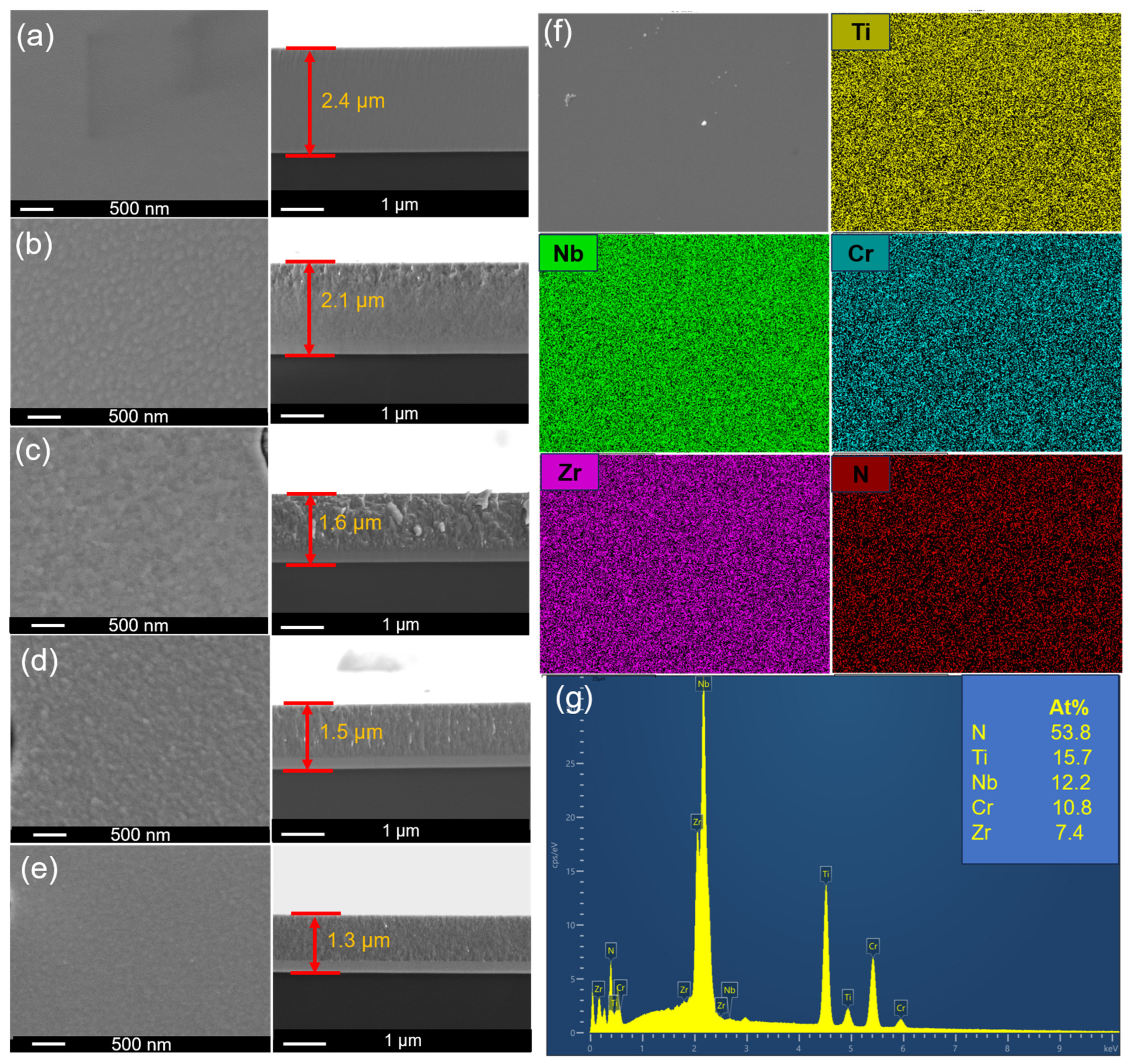
Figure 3a–e presents the surface and cross-section morphologies of the (TiNbZrCr)Nx HENFs deposited at different FN. The film thickness gradually decreases with the increase in the FN, which is mainly caused by “target poisoning”. The nitride layer formed on the target surface makes it more difficult for atoms to be sputtered out, which ultimately leads to a decrease in sputtering yield. As the FN increases, the surface of the film changes from a smooth morphology at FN = 0 sccm to a rough granular morphology at FN = 4, 8, 12, and 16 sccm. The cross-sectional morphology of the HENFs deposited at FN = 0 sccm shows a dense structure. The cross-sectional morphologies of the HENFs deposited at FN = 4, 8, 12, and 16 sccm show a dense transition layer and a columnar structure of the nitride layer. All nitride films present a dense structure, with no clear boundaries between columnar crystals, which is mainly attributed to the high ionization rate and high energy of the sputtered particles. Figure 3f,g shows the EDS mapping and composition ratio of the (TiNbZrCr)Nx HENFs deposited at FN = 12 sccm. The composition of the HENFs is uniformly distributed, and no segregation is observed.
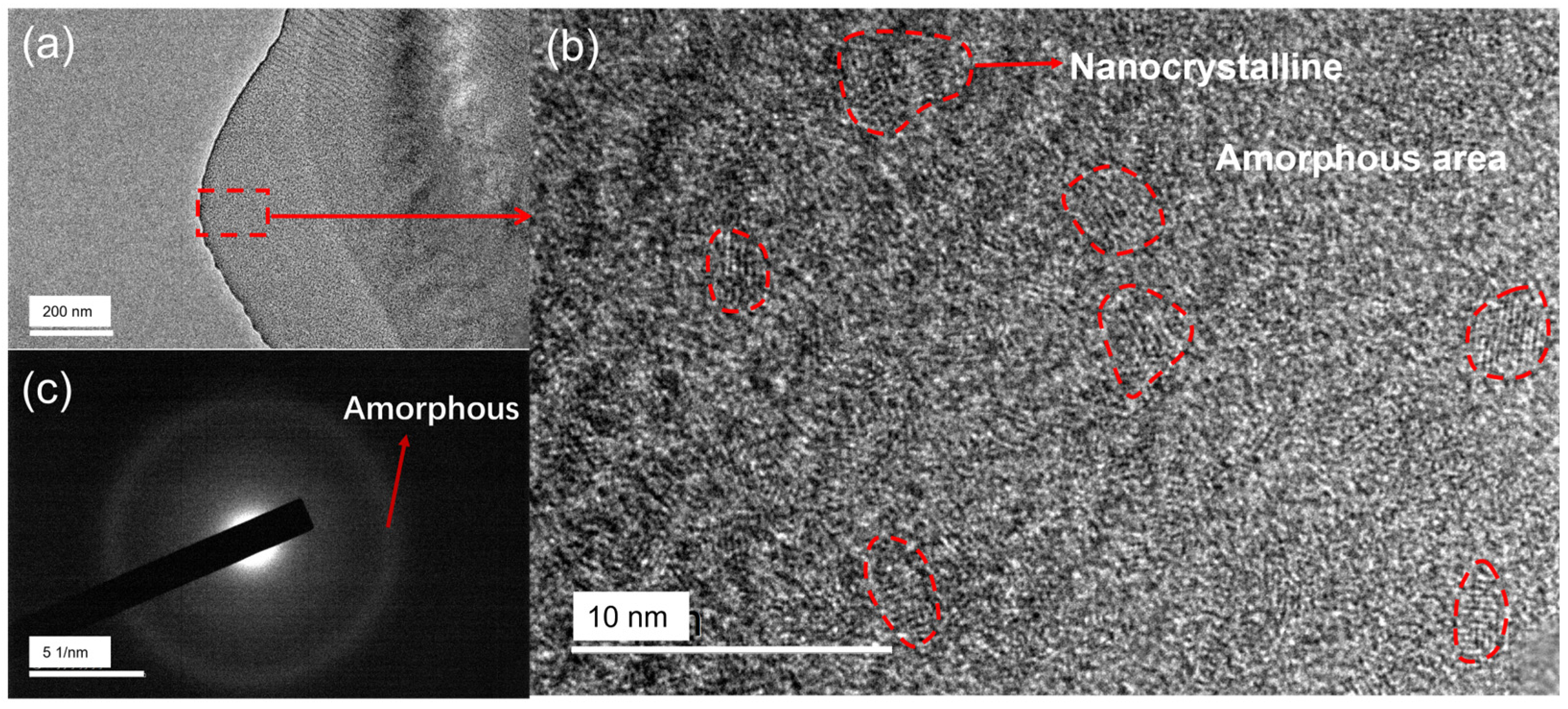
Figure 4 shows the TEM images of the (TiNbZrCr)Nx HENFs deposited at FN = 12 sccm. Figure 4a is the low-magnified image, and we select the area within the dashed box for high-resolution TEM analysis. As shown in Figure 4b, the high-resolution image of the thin film shows a large number of grains with a size of approximately 5 nm distributed in the disordered matrix. Figure 4c presents the selected area electron diffraction image, and the result shows that there is only one halo, which is related to the amorphous phase. This may be because the proportion of the amorphous phase is significant so that the electron diffraction pattern of nanocrystals does not appear. The above results indicate that the thin film is an amorphous-nanocrystalline nanocomposite structure. It is speculated that the formation of this structure is related to the enhancement of particle bombardment. With the increase in the N2 fraction, plasma discharge is enhanced, and the bombardment effect of deposited particles on the substrate is enhanced. The emergence of amorphous-nanocrystalline structures is accompanied by a decrease in grain size, which is related to the enhancement of the bombardment effect. Under low bombardment, larger grain sizes can be obtained. As the bombardment increases, crystal growth is hindered by the defects and, thus, defects contribute to the nucleation of grains, ultimately forming a composite structure of a large number of small grains and amorphous defects.
3.3. Mechanical and Tribological Properties of the (TiNbZrCr)Nx HENFs
Appropriate film stress can increase the hardness of the film by restricting plastic deformation and dislocation movement [24]. However, excessive stress will cause the film delamination when the film thickness increases. The residual stress of (TiNbZrCr)Nx HENFs is shown in Figure 5a. As the FN increases, the residual stress of the HENFs gradually increases, and at FN = 8 sccm, the compressive stress reaches a maximum of 2.37 GPa. As the FN increases to 12 and 16 sccm, the compressive stress of the film decreases slightly. The residual stress of the film usually includes thermal stress and intrinsic stress [25]. Since magnetron sputtering is considered a low-temperature deposition process and no additional heating during the film deposition, the residual stress in the HENFs mainly comes from the intrinsic stress, which is caused by the internal structure and defects of the film. The increase in compressive stress is related to the bombardment effect of particles. High energy particles bombarding the growing thin film can cause lattice distortion, and implanting particles can generate compressive stress [26,27]. The subsequent decrease in stress is attributed to the formation of amorphous nanocrystalline structures. The appearance of amorphous phases will absorb a portion of strain energy, thereby releasing stress to a certain extent [28].
Figure 5b is the hardness and Young’s modulus of the (TiNbZrCr)Nx HENFs. As there is an increase in FN, the hardness and Young’s modulus of the HENFs gradually increase and reach their maximum value at FN = 8 sccm, which are 27.8 GPa and 247.8 GPa, respectively. The increase in hardness is attributed to the formation of nano-sized nitride phases. The strong Me-N covalent bonds in the HENFs are conducive to an increase in film hardness. In addition, the fine grain strengthening effect and the interface strengthening effect are also important factors in the increase in hardness. The subsequent decrease in hardness is related to the decrease in grain size. When the grain size is below 10 nm, the grain boundary slip occurs and softens the material, which is known as the inverse Hall–Petch effect. Residual stress can also affect the film hardness [25,29]. In this research, the variation trend of residual stress is similar to that of hardness. In general, compressive stress can inhibit the indentation of the indenter, thereby increasing the measured hardness of the film.
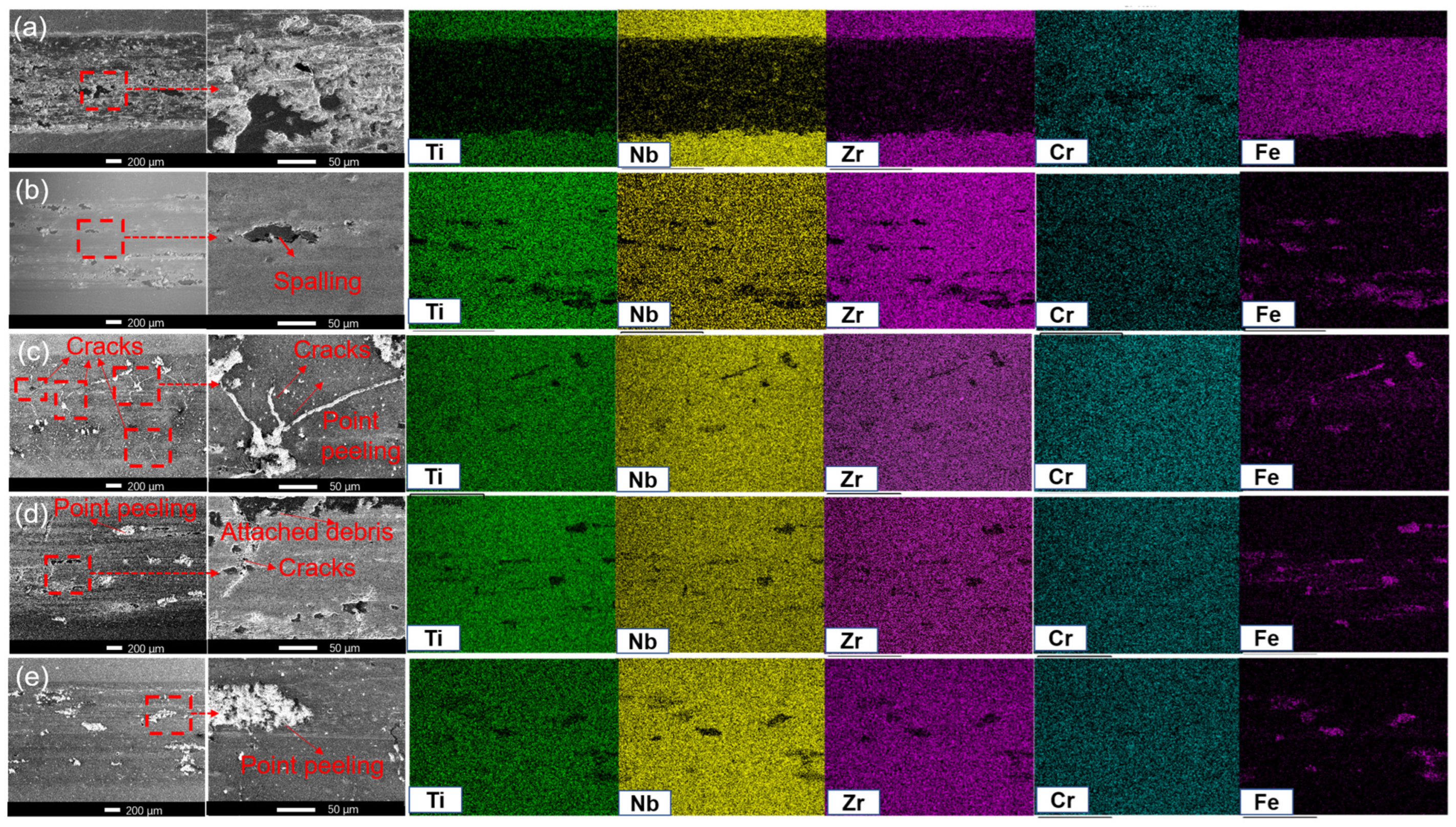
The results of the friction coefficient (COF) curves and the average value of the (TiNbZrCr)Nx HENFs are given in Figure 6a,b. The COF of the (TiNbZrCr)Nx HENFs decreases from 0.75 to 0.51 with the increase in FN. The profiles of the wear scar and the calculated wear rate are shown in Figure 6c and d, respectively. After the introduction of N atoms into the HENFs, the depth of the wear scar is significantly reduced. The calculated wear rate also shows that the wear rate of the HENFs decreases by a factor of magnitude after the introduction of N atoms into the HENFs, from 10−5 to 10−6 mm3N−1m−1. The wear rate of the HENFs deposited at FN = 12 sccm reaches the lowest at 4.0 × 10⁻⁶ mm3N−1m−1. To further investigate the friction mechanism of the film, the morphologies and composition of the wear tracks of the (TiNbZrCr)Nx HENFs are studied, and the results are shown in Figure 7. HENFs deposited at FN = 0 sccm show that the film has almost worn through and failed. The HENFs deposited at FN = 4 sccm show obvious local peeling (as can be seen from the exposure of Fe elements in the matrix). The HENFs deposited at FN = 8 sccm show a large number of cracks at the wear track, and there is a point peeling at the center of the cracks, which indicates the films exhibit fatigue wear. The nanocomposite HENFs deposited at FN = 12 sccm show reduced cracks, but the film still exhibits point peeling. The nanocomposite HENFs deposited at FN = 16 sccm are similar to that of film deposited at 12 sccm. The above results show that the HENFs prepared at FN = 12 sccm have the most excellent tribological properties. In general, the tribological properties are related to the hardness and toughness of the film [30]. High hardness can prevent the pressing of the grinding pair, while excellent toughness can reduce cracks and reduce the risk of brittle peeling failure of the film through coordinated deformation. Therefore, the nanocomposite structure of HENFs deposited at FN = 12 sccm enables it to have a certain increase in toughness on the basis of high hardness, which significantly reduces the number of cracks. And the combination of high hardness and toughness maximizes its tribological performance.
3.4. Corrosion Resistance of the (TiNbZrCr)Nx HENFs
The Nyquist plots (Figure 8a) and Bode plots (Figure 8b,c) of the (TiNbZrCr)Nx HENFs and the 316 SS substrate obtained from the electrochemical impedance test are shown in Figure 8. The points in Figure 8 are the actual data of the impedance test, and the straight lines are the fitting results. The matched equivalent circuit diagram of samples is also shown in Figure 8d, where Rs, Rp, and Rct represent the solution resistance, the film resistance, and the substrate polarization resistance, respectively. The CPEp and CPEct are the constant phase elements of the HENFs and substrate, respectively. The above fitting parameters are summarized in Table 3. And the χ2 in Table 3 is the degree of fit, and generally, the smaller the value, the higher the degree of fit. For the Nyquist plots (Figure 8a), the diameter of the semicircles represents the charge transfer resistance (Rct). A larger diameter indicates a larger RCT. It can be seen that, with the increase in FN, the Rct of HENFs first decreases and then increases. The value of |Z| at a frequency of 0.01 Hz is usually used to reflect the corrosion resistance of the film. It can be seen from Figure 8b that with the increase in FN, the corrosion resistance of the HENFs first decreases and then increases, with the best corrosion resistance at FN = 0 sccm and the worst corrosion resistance at FN = 8 sccm. The corrosion resistance of the HENFs obtained from the Nyquist diagram is consistent with that from the Bode plot. It can be seen from Figure 8c that all HENF-coated samples have two-time constants. The Rp + Rct is the total impedance, which can represent the comprehensive corrosion resistance performance of the thin film [31,32]. The larger total impedance represents better corrosion resistance. As FN increases, the total impedance first decreases and then increases.
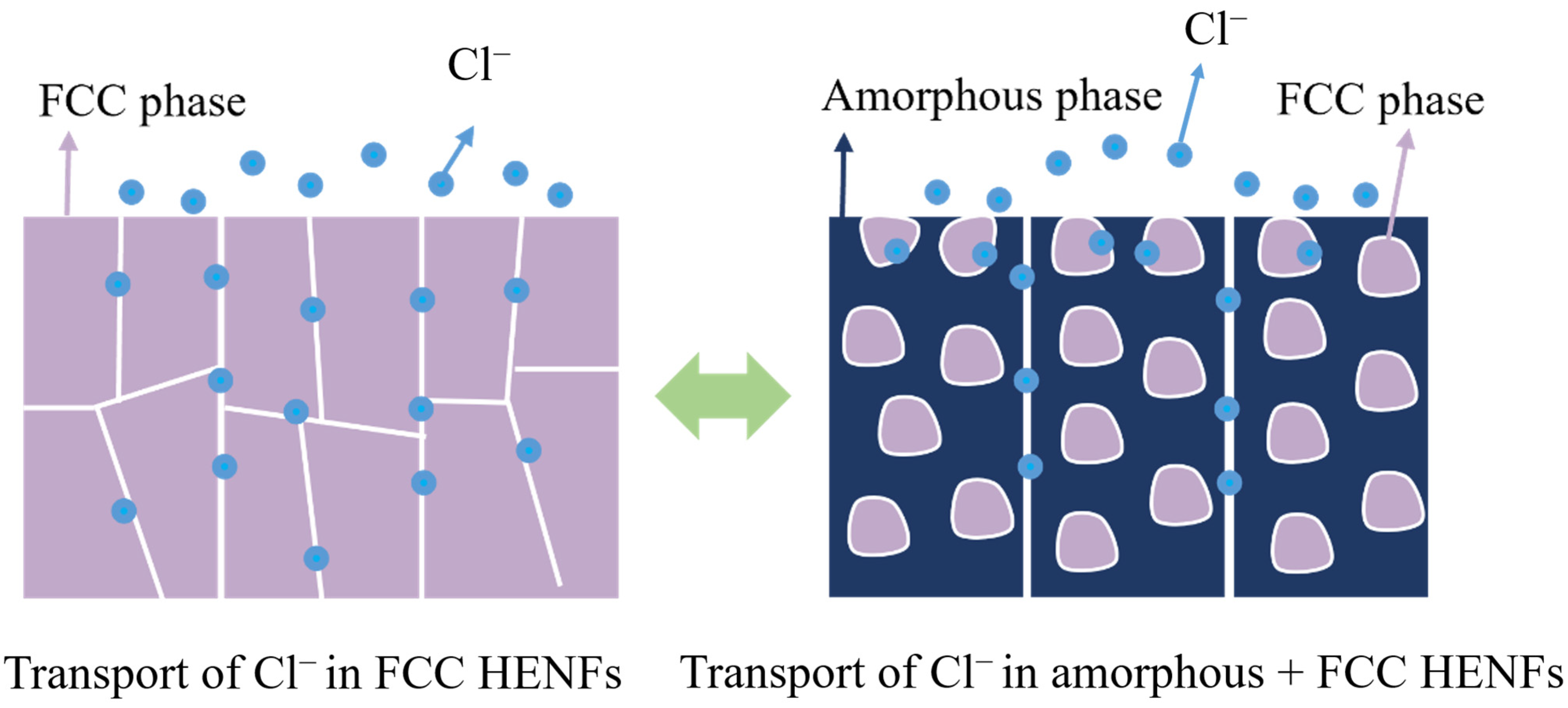
Figure 9 shows the polarization curves of 316 SS substrate and (TiNbZrCr)Nx HENFs prepared at different FN. All curves of HENFs directly transition from the Tafel region to a stable passive region without showing a transition from active to passive, indicating that the protective layer is spontaneously formed with the corrosion potential. The corrosion potential (Ecorr) and corrosion current density (Icorr) shown in Table 4 are obtained by the Tafel curve extrapolation method. Ecorr is the open-circuit potential, reflecting the corrosion tendency of the samples [33]. The Ecorr of the HENFs prepared at FN = 4 sccm shows a minimal corrosion tendency. Icorr generally represents the corrosion rate of samples [34]. The (TiNbZrCr)Nx HENFs exhibit low corrosion currents, comparable to 316 stainless steel substrates, indicating excellent corrosion resistance. The HENFs deposited at FN = 0 sccm exhibit the lowest corrosion current (4.64 × 10⁻⁹ A/cm2), which is lower than the 316 stainless steel, indicating the most excellent corrosion resistance. Above all, the corrosion resistance of the HENFs is closely related to the structure of the HENFs. At FN = 0 sccm, the film is amorphous and exhibits excellent corrosion resistance. With the increase in FN, the film transforms into a columnar FCC structure, and its corrosion resistance decreases. With the further increase in FN, the film transforms into an amorphous + FCC composite structure, and the corrosion resistance of the film improves. It is reported that amorphous structures can significantly improve the corrosion resistance of high-entropy alloy films [35]. As shown in Figure 10, in FCC nitride films, grain boundaries and columnar structure gaps become Cl−-transport channels, resulting in an increased corrosion rate. In the amorphous-nanocrystalline composite HENFs, Cl− can only be transferred through the columnar structure gap, which reduces the transmission channel of Cl− and thus reduces the corrosion rate. In conclusion, the amorphization of high-entropy nitride films is beneficial to the improvement of corrosion resistance.
4. Conclusions
In this study, (TiNbZrCr)Nx high-entropy nitride films were prepared using high-power pulsed magnetron sputtering technology by changing the nitrogen flow rate. The microstructure, residual stress, hardness, tribological properties, and corrosion resistance of the (TiNbZrCr)Nx films were investigated. The main conclusions are summarized as follows:
- With the increase in N2 flow rate, the (TiNbZrCr)Nx films first form an FCC structure, and then transform into an amorphous + nanocrystalline composite structure, which is attributed to the enhanced ion bombardment effect.
- The (TiNbZrCr)Nx films deposited at FN = 8 sccm show the highest hardness of 27.8 GPa, and the (TiNbZrCr)Nx films deposited at FN = 12 sccm exhibit the best wear resistance, with a wear rate of 4.0 × 10⁻⁶ mm3N−1m−1.
- Compared with FCC (TiNbZrCr)Nx films, the (TiNbZrCr)Nx films with amorphous-nanocrystalline structure show excellent corrosion resistance, with corrosion current dropping to 1.72 × 10⁻⁸ A/cm2.
Author Contributions
Conceptualization, D.M.; methodology, Y.L. (Yantao Li); software, J.L., D.H., L.W.; validation, Y.L. (Yantao Li), D.M. and J.L.; formal analysis, Y.L. (Yantao Li); investigation, Y.L. (Yantao Li), D.H., L.W. and D.R.; resources, J.L., Y.L. (Yongxiang Leng) and X.J.; data curation, Y.L. (Yantao Li); writing—original draft preparation, Y.L. (Yantao Li) and D.M.; writing—review and editing, Y.L. (Yantao Li), D.M., X.J. and Y.L. (Yongxiang Leng); visualization, Y.L. (Yantao Li) and D.M.; supervision, D.M.; project administration, X.J.; funding acquisition, J.L., Y.L. (Yongxiang Leng) and X.J. All authors have read and agreed to the published version of the manuscript.
Funding
This work was supported by the National Natural Science Foundation of China (Grant Nos. 51975564 and 52375206), the Sichuan Provincial Department of Science and Technology (Grant Nos. 2022065 and 2023YFG0246), the Sichuan College Student Innovation Training Program (S202314389094).
Institutional Review Board Statement
Not applicable.
Informed Consent Statement
Not applicable.
Data Availability Statement
Data available on request from the authors.
Conflicts of Interest
The authors declare no conflict of interest.
References
- Li, W.; Liu, P.; Liaw, P.K. Microstructures and properties of high-entropy alloy films and coatings: A review. Mater. Res. Lett. 2018, 6, 199–229. [Google Scholar] [CrossRef]
- Feng, X.; Zhang, J.; Xia, Z.; Fu, W.; Wu, K.; Liu, G.; Sun, J. Stable nanocrystalline NbMoTaW high entropy alloy thin films with excellent mechanical and electrical properties. Mater. Lett. 2018, 210, 84–87. [Google Scholar] [CrossRef]
- Xu, Y.; Li, G.; Xia, Y. Synthesis and characterization of super-hard AlCrTiVZr high-entropy alloy nitride films deposited by HiPIMS. Appl. Surf. Sci. 2020, 523, 146529. [Google Scholar] [CrossRef]
- Cheng, K.H.; Lai, C.H.; Lin, S.J.; Yeh, J.W. Structural and mechanical properties of multi-element (AlCrMoTaTiZr)Nx coatings by reactive magnetron sputtering. Thin Solid Film. 2011, 519, 3185–3190. [Google Scholar] [CrossRef]
- Wang, J.; Kuang, S.; Yu, X.; Wang, L.; Huang, W. Tribo-mechanical properties of CrNbTiMoZr high-entropy alloy film synthesized by direct current magnetron sputtering. Surf. Coat. Technol. 2020, 403, 126374. [Google Scholar] [CrossRef]
- Wang, Z.; Chen, F.; Dong, Y.; Cai, Z.; Zhang, P.; Chen, J.; Gu, L.; Zeng, L. Effect of heat-treatment time on microstructure and tribological behavior of (TiVCrAlMo)N high-entropy alloy films. Surf. Coat. Technol. 2022, 443, 128618. [Google Scholar] [CrossRef]
- Alvi, S.; Jarzabek, D.M.; Kohan, M.G.; Hedman, D.; Akhtar, F. Synthesis and Mechanical Characterization of a CuMoTaWV High-Entropy Film by Magnetron Sputtering. ACS Appl. Mater. Interfaces 2020, 12, 21070–21079. [Google Scholar] [CrossRef] [PubMed]
- Chang, F.; Cai, B.; Zhang, C.; Huang, B.; Li, S.; Dai, P. Thermal stability and oxidation resistance of FeCrxCoNiB high-entropy alloys coatings by laser cladding. Surf. Coat. Technol. 2019, 359, 132–140. [Google Scholar] [CrossRef]
- Lu, C.; Niu, L.; Chen, N.; Jin, K.; Yang, T.; Xiu, P.; Zhang, Y.; Gao, F.; Bei, H.; Shi, S.; et al. Enhancing radiation tolerance by controlling defect mobility and migration pathways in multicomponent single-phase alloys. Nat. Commun. 2016, 7, 13564. [Google Scholar] [CrossRef]
- Lu, C.; Yang, T.; Jin, K.; Gao, N.; Xiu, P.; Zhang, Y.; Gao, F.; Bei, H.; Weber, W.J.; Sun, K.; et al. Radiation-induced segregation on defect clusters in single-phase concentrated solid-solution alloys. Acta Mater. 2017, 127, 98–107. [Google Scholar] [CrossRef]
- Zheng, S.; Cai, Z.; Pu, J.; Zeng, C.; Wang, L. Passivation behavior of VAlTiCrSi amorphous high-entropy alloy film with a high corrosion-resistance in artificial sea water. Appl. Surf. Sci. 2021, 542, 148520. [Google Scholar] [CrossRef]
- Wang, R.; Zhang, K.; Davies, C.; Wu, X. Evolution of microstructure, mechanical and corrosion properties of AlCoCrFeNi high-entropy alloy prepared by direct laser fabrication. J. Alloys Compd. 2017, 694, 971–981. [Google Scholar] [CrossRef]
- Liu, X.; Cai, W.; Zhang, Y.; Wang, L.; Wang, J. Tuning microstructure and mechanical and wear resistance of ZrNbTiMo refractory high-entropy alloy films via sputtering power. Front. Mater. 2023, 10, 1145631. [Google Scholar] [CrossRef]
- Braeckman, B.R.; Misják, F.; Radnóczi, G.; Caplovicová, M.; Djemia, P.; Tétard, F.; Belliard, L.; Depla, D. The nanostructure and mechanical properties of nanocomposite Nbx-CoCrCuFeNi thin films. Scr. Mater. 2017, 139, 155–158. [Google Scholar] [CrossRef]
- Yu, W.; Li, W.; Liu, P.; Zhang, K.; Ma, F.; Chen, X.; Feng, R.; Liaw, P.K. Silicon-content-dependent microstructures and mechanical behavior of (AlCrTiZrMo)-Six-N high-entropy alloy nitride films. Mater. Des. 2021, 203, 109553. [Google Scholar] [CrossRef]
- Li, Y.T.; Wang, C.T.; Ma, D.L.; Zeng, X.K.; Liu, M.; Jiang, X.; Leng, Y.X. Nano dual-phase CuNiTiNbCr high entropy alloy films produced by high-power pulsed magnetron sputtering. Surf. Coat. Technol. 2021, 420, 127325. [Google Scholar] [CrossRef]
- Oks, E.; Anders, A. Evolution of the plasma composition of a high power impulse magnetron sputtering system studied with a time-of-flight spectrometer. J. Appl. Phys. 2009, 105, 093304. [Google Scholar] [CrossRef]
- Oliveira, J.C.; Fernandes, F.; Serra, R.; Cavaleiro, A. On the role of the energetic species in TiN thin film growth by reactive deep oscillation magnetron sputtering in Ar/N2. Thin Solid Films. 2018, 645, 253–264. [Google Scholar] [CrossRef]
- Anders, A. Discharge physics of high power impulse magnetron sputtering. Surf. Coat. Technol. 2011, 205, S1–S9. [Google Scholar] [CrossRef]
- Gudmundsson, J.; Magnus, F.; Sveinsson, O.; Olafsson, S. Current-voltage-time characteristics of the reactive Ar/N2 high power impulse magnetron sputtering discharge. J. Appl. Phys. 2011, 110, 083306. [Google Scholar] [CrossRef]
- Zhao, Y.; Chen, S.; Chen, Y.; Wu, S.; Xie, W.; Yan, W.; Wang, S.; Liao, B.; Zhang, S. Super-hard and anti-corrosion (AlCrMoSiTi)Nx high entropy nitride coatings by multi-arc cathodic vacuum magnetic filtration deposition. Vacuum 2022, 195, 110685. [Google Scholar] [CrossRef]
- Ren, B.; Zhao, R.F.; Zhang, G.P.; Liu, Z.X.; Cai, B.; Jiang, A.Y. Microstructure and properties of the AlCrMoZrTi/(AlCrMoZrTi)N multilayer high-entropy nitride ceramics films deposited by reactive RF sputtering. Ceram. Int. 2022, 48, 16901–16911. [Google Scholar] [CrossRef]
- Cui, P.; Li, W.; Liu, P.; Zhang, K.; Ma, F.; Chen, X.; Feng, R.; Liaw, P.K. Effects of nitrogen content on microstructures and mechanical properties of (AlCrTiZrHf)N high-entropy alloy nitride films. J. Alloys Compd. 2020, 834, 155063. [Google Scholar] [CrossRef]
- Lin, J.; Moore, J.J.; Mishra, B.; Pinkas, M.; Sproul, W.D.; Rees, J.A. Effect of asynchronous pulsing parameters on the structure and properties of CrAlN films deposited by pulsed closed field unbalanced magnetron sputtering (P-CFUBMS). Surf. Coat. Technol. 2008, 202, 1418–1436. [Google Scholar] [CrossRef]
- Hsieh, M.H.; Tsai, M.H.; Shen, W.J.; Yeh, J.W. Structure and properties of two Al–Cr–Nb–Si–Ti high-entropy nitride coatings. Surf. Coat. Technol. 2013, 221, 118–123. [Google Scholar] [CrossRef]
- Bilek, M.M.M.; Mckenzie, D.R. A comprehensive model of stress generation and relief processes in thin films deposited with energetic ions. Surf. Coat. Technol. 2006, 200, 4345–4354. [Google Scholar] [CrossRef]
- Bielawski, M. Residual stress control in TiN/Si coatings deposited by unbalanced magnetron sputtering. Surf. Coat. Technol. 2006, 200, 3987–3995. [Google Scholar] [CrossRef]
- Li, Y.T.; Chen, X.M.; Zeng, X.K.; Liu, M.; Jiang, X.; Leng, Y.X. Hard yet tough and self-lubricating (CuNiTiNbCr)Cx high-entropy nanocomposite films: Effects of carbon content on structure and properties. J. Mater. Sci. Technol. 2024, 173, 20–30. [Google Scholar] [CrossRef]
- Lo, W.L.; Hsu, S.Y.; Lin, Y.C.; Tsai, S.Y.; Lai, Y.T.; Duh, J.G. Improvement of high entropy alloy nitride coatings (AlCrNbSiTiMo)N on mechanical and high temperature tribological properties by tuning substrate bias. Surf. Coat. Technol. 2020, 401, 126247. [Google Scholar] [CrossRef]
- Liu, C.; Li, Z.; Lu, W.; Bao, Y.; Xia, W.; Wu, X.; Zhao, H.; Gault, B.; Liu, C.; Herbig, M.; et al. Reactive wear protection through strong and deformable oxide nanocomposite surfaces. Nat. Commun. 2021, 12, 5518. [Google Scholar] [CrossRef]
- Zeng, X.K.; Li, Y.T.; Zhang, X.D.; Liu, M.; Ye, J.Z.; Qiu, X.L.; Jiang, X.; Leng, Y.X. Effect of bias voltage on the structure and properties of CuNiTiNbCr dual-phase high entropy alloy films. J. Alloys Compd. 2023, 931, 167371. [Google Scholar] [CrossRef]
- Yu, X.; Wang, J.; Wang, L.; Huang, W. Fabrication and characterization of CrNbSiTiZr high-entropy alloy films by radio-frequency magnetron sputtering via tuning substrate bias. Surf. Coat. Technol. 2021, 412, 127074. [Google Scholar] [CrossRef]
- Wang, Z.; Li, D.Y.; Yao, Y.Y.; Kuo, Y.L.; Hsueh, C.H. Wettability, electron work function and corrosion behavior of CoCrFeMnNi high entropy alloy films. Surf. Coat. Technol. 2020, 400, 126222. [Google Scholar] [CrossRef]
- Jiang, K.M.; Zhao, D.Q.; Jiang, X.; Huang, Q.; Miao, L.J.; Lu, H.M.; Li, Y. Electronic-structure, corrosion and mechanical properties of nc-CrC/a-C:H films deposited by multi-arc ion plating. J. Alloys Compd. 2018, 750, 560–569. [Google Scholar] [CrossRef]
- Zheng, S.; Cai, Z.; Pu, J.; Zeng, C.; Chen, S.; Chen, R.; Wang, L. A feasible method for the fabrication of VAlTiCrSi amorphous high entropy alloy film with outstanding anti-corrosion property. Appl. Surf. Sci. 2019, 483, 870–874. [Google Scholar] [CrossRef]
Figure 1.
(a) The HPPMS discharge voltage and current and (b) the composition of the (TiNbZrCr)Nx HENFs deposited at different nitrogen flow rates.
Figure 1.
(a) The HPPMS discharge voltage and current and (b) the composition of the (TiNbZrCr)Nx HENFs deposited at different nitrogen flow rates.

Figure 2.
XRD spectra of (TiNbZrCr)Nx HENFs deposited at different nitrogen flow rates.

Figure 3.
SEM surface and cross-section morphologies of (TiNbZrCr)Nx HENFs deposited at FN = (a) 0 sccm, (b) 4 sccm, (c) 8 sccm, (d) 12 sccm, (e) 16 sccm, (f) the EDS-mapping, and (g) the elemental ratio of (TiNbZrCr)Nx HENFs deposited at FN = 12 sccm.
Figure 3.
SEM surface and cross-section morphologies of (TiNbZrCr)Nx HENFs deposited at FN = (a) 0 sccm, (b) 4 sccm, (c) 8 sccm, (d) 12 sccm, (e) 16 sccm, (f) the EDS-mapping, and (g) the elemental ratio of (TiNbZrCr)Nx HENFs deposited at FN = 12 sccm.

Figure 4.
TEM images of (TiNbZrCr)Nx deposited at 12 sccm N2: (a) low-magnified images, (b) high-resolution image, and (c) selected area electron diffraction pattern.
Figure 4.
TEM images of (TiNbZrCr)Nx deposited at 12 sccm N2: (a) low-magnified images, (b) high-resolution image, and (c) selected area electron diffraction pattern.

Figure 5.
(a) Residual stress, (b) hardness (blue dash line), and Young’s modulus (red dash line) of (TiNbZrCr)Nx HENFs deposited at different nitrogen flow rates.
Figure 5.
(a) Residual stress, (b) hardness (blue dash line), and Young’s modulus (red dash line) of (TiNbZrCr)Nx HENFs deposited at different nitrogen flow rates.

Figure 6.
(a) Friction coefficient curves, (b) average friction coefficients, (c) wear track profiles, and (d) wear rates of (TiNbZrCr)Nx HENFs deposited at different nitrogen flow rates.
Figure 6.
(a) Friction coefficient curves, (b) average friction coefficients, (c) wear track profiles, and (d) wear rates of (TiNbZrCr)Nx HENFs deposited at different nitrogen flow rates.

Figure 7.
Wear track morphologies and composition distribution of (TiNbZrCr)Nx HENFs deposited at FN = (a) 0 sccm, (b) 4 sccm, (c) 8 sccm, (d) 12 sccm, and (e) 16 sccm.
Figure 7.
Wear track morphologies and composition distribution of (TiNbZrCr)Nx HENFs deposited at FN = (a) 0 sccm, (b) 4 sccm, (c) 8 sccm, (d) 12 sccm, and (e) 16 sccm.

Figure 8.
(a) Nyquist, (b) and (c) Bode plots from EIS data of 316 SS and (TiNZrCr)Nx HENFs. (d) Equivalent circuit model of the substrate and HENFs coated substrate.
Figure 8.
(a) Nyquist, (b) and (c) Bode plots from EIS data of 316 SS and (TiNZrCr)Nx HENFs. (d) Equivalent circuit model of the substrate and HENFs coated substrate.

Figure 9.
Potentiodynamic polarization curves of bare 316 SS and the (TiNbZrCr)Nx HENFs in 3.5 wt.% NaCl.
Figure 9.
Potentiodynamic polarization curves of bare 316 SS and the (TiNbZrCr)Nx HENFs in 3.5 wt.% NaCl.

Figure 10.
Schematic diagram of chloride ion transport in FCC and amorphous + FCC HENFs.


Table 1.
Deposition parameters of the (TiNbZrCr)Nx HENFs.
| Films | Bias Voltage /V | Ar /sccm | N2 /sccm | Power Source (Graphite) /V-μs-Hz | Deposition Pressure /Pa | Deposition Time /min |
|---|---|---|---|---|---|---|
| H1-0 sccm | −60 | 40 | 0 | 800-150-200 | 0.54 | 32 |
| H2-4 sccm | −60 | 40 | 4 | 800-150-200 | 0.55 | 32 |
| H3-8 sccm | −60 | 40 | 8 | 800-150-200 | 0.55 | 32 |
| H4-12 sccm | −60 | 40 | 12 | 800-150-200 | 0.55 | 32 |
| H5-16 sccm | −60 | 40 | 16 | 800-150-200 | 0.56 | 32 |
Table 2.
The grain sizes of (TiNbZrCr)N films.
| Samples/Parameter | 0 sccm | 4 sccm | 8 sccm | 12 sccm | 16 sccm |
|---|---|---|---|---|---|
| Grain size (nm) | - | 26.0 | 18.0 | 14.5 | 7.5 |
Table 3.
Electrochemical impedance parameters obtained by fitting EIS data of the HENFs and 316 SS substrate.
Table 3.
Electrochemical impedance parameters obtained by fitting EIS data of the HENFs and 316 SS substrate.
| Samples/ Parameter | Rs (Ω·cm2) | Rp (Ω·cm2) | CPEp (sn·Ω−1·cm−2) | Rct (Ω−1·cm2) | CPEct (sn·Ω−1·cm−2) | χ2 |
|---|---|---|---|---|---|---|
| 0 sccm | 19.5 | 10,779 | 1.6 × 10⁻⁵ | 644,100 | 7.3 × 10⁻⁶ | 0.0088 |
| 4 sccm | 20.6 | 3150 | 1.5 × 10⁻⁵ | 359,450 | 8.6 × 10⁻⁶ | 0.0098 |
| 8 sccm | 20.4 | 10,705 | 2.2 × 10⁻⁵ | 137,930 | 1.7 × 10⁻⁵ | 0.0072 |
| 12 sccm | 19.5 | 2236 | 2.9 × 10⁻⁵ | 195,350 | 1.9 × 10⁻⁵ | 0.0076 |
| 16 sccm | 19.5 | 8792 | 2.3 × 10⁻⁵ | 497,290 | 1.2 × 10⁻⁵ | 0.0074 |
| 316 SS | 19.4 | - | - | 902,090 | 4.1 × 10⁻⁵ | 0.0162 |
Table 4.
The corrosion potential (Ecorr) and corrosion current density (Icorr) for the HENFs-coated and uncoated 316 SS.
Table 4.
The corrosion potential (Ecorr) and corrosion current density (Icorr) for the HENFs-coated and uncoated 316 SS.
| Samples | 316 SS | 0 sccm | 4 sccm | 8 sccm | 12 sccm | 16 sccm |
|---|---|---|---|---|---|---|
| Ecorr (VSCE) | −0.12 | −0.25 | −0.11 | −0.18 | −0.23 | −0.24 |
| Icorr (A/cm2) | 1.99 × 10⁻⁸ | 4.64 × 10⁻⁹ | 1.75 × 10⁻⁸ | 3.16 × 10⁻⁸ | 2.14 × 10⁻⁸ | 1.72 × 10⁻⁸ |
Disclaimer/Publisher’s Note: The statements, opinions and data contained in all publications are solely those of the individual author(s) and contributor(s) and not of MDPI and/or the editor(s). MDPI and/or the editor(s) disclaim responsibility for any injury to people or property resulting from any ideas, methods, instructions or products referred to in the content. |
© 2024 by the authors. Licensee MDPI, Basel, Switzerland. This article is an open access article distributed under the terms and conditions of the Creative Commons Attribution (CC BY) license (https://creativecommons.org/licenses/by/4.0/).
Share and Cite
MDPI and ACS Style
Li, Y.; Ma, D.; Liang, J.; Huang, D.; Wang, L.; Ren, D.; Jiang, X.; Leng, Y. Plasma Bombardment-Induced Amorphization of (TiNbZrCr)Nx High-Entropy Alloy Nitride Films. Coatings 2024, 14, 505. https://doi.org/10.3390/coatings14040505
AMA Style
Li Y, Ma D, Liang J, Huang D, Wang L, Ren D, Jiang X, Leng Y. Plasma Bombardment-Induced Amorphization of (TiNbZrCr)Nx High-Entropy Alloy Nitride Films. Coatings. 2024; 14(4):505. https://doi.org/10.3390/coatings14040505
Chicago/Turabian StyleLi, Yantao, Donglin Ma, Jun Liang, Deming Huang, Libo Wang, Diqi Ren, Xin Jiang, and Yongxiang Leng. 2024. "Plasma Bombardment-Induced Amorphization of (TiNbZrCr)Nx High-Entropy Alloy Nitride Films" Coatings 14, no. 4: 505. https://doi.org/10.3390/coatings14040505
Note that from the first issue of 2016, this journal uses article numbers instead of page numbers. See further details here.