Concept Paper

Metallization on FDM Parts Using the Chemical Deposition Technique

Manufacturing Engineering, National Institute of Foundry and Forge Technology, Ranchi 834003, India
*
Author to whom correspondence should be addressed.
Coatings 2014, 4(3), 574-586; https://doi.org/10.3390/coatings4030574
Submission received: 7 May 2014 / Revised: 14 July 2014 / Accepted: 21 July 2014 / Published: 5 August 2014

Abstract

:
Metallization of ABS (acrylonitrile-butadiene-styrene) parts has been studied on flat part surfaces. These parts are fabricated on an FDM (fused deposition modeling machine) using the layer-wise deposition principle using ABS as a part material. Electroless copper deposition on ABS parts was performed using two different surface preparation processes, namely ABS parts prepared using chromic acid for etching and ABS parts prepared using a solution mixture of sulphuric acid and hydrogen peroxide (H2SO4/H2O2) for etching. After surface preparations using these routes, copper (Cu) is deposited electrolessly using four different acidic baths. The acidic baths used are 5 wt% CuSO4 (copper sulfate) with 15 wt% of individual acids, namely HF (hydrofluoric acid), H2SO4 (sulphuric acid), H3PO4 (phosphoric acid) and CH3COOH (acetic acid). Cu deposition under different acidic baths used for both the routes is presented and compared based on their electrical performance, scanning electron microscopy (SEM) and energy dispersive X-ray spectrometry (EDS). The result shows that chromic acid etched samples show better electrical performance and Cu deposition in comparison to samples etched via H2SO4/H2O2.

1. Introduction

Plastic has many attractive properties, which include light weight, easy formability, reflectivity, abrasion resistance, electrical conductivity, etc. However, there are many areas in which, due to decorative or technological considerations, metallic properties are required or demanded [1]. It is in these applications that the possibility of metalizing plastics has opened the door to new uses for these materials. Metallization is a process in which a non-conductive material, such as plastic, is made conductive by providing a conductive layer on it. With metallization, the physical and mechanical properties of plastics, such as reflectivity, heat resistance, strength, etc., can be improved or may be changed as desired [2]. This has increased the possibility of utilizing the properties of metal and plastic in the same part material. As a result, plated plastic is used to address a variety of needs, from decorative finishes, such as chrome-plated automotive trim used in interior and exterior applications, automobile parts (such as dashes, dash boards, arm rests, vents, etc.) to functional requirements, such as controlling electro-magnetic emissions from electronic industries.
A variety of plastics, such as polythene, Teflon, polysulfone, polypropylene, acrylonitrile-butadiene-styrene (ABS), etc. can be metalized with different metals, like copper (Cu), zinc (Zn), nickel (Ni), gold (Au), chromium (Cr), silver (Ag), etc. [3,4]. Having excellent electrical conductivity and being relatively inexpensive, Cu has been widely studied for metallization, and a variety of plastics have been plated. The different metallization process involves electroless plating, brushing a metal paint, the spray metal technique, dipping in a metal paint, sputtering and vacuum metallization [5,6,7,8]. Among these, electroless plating, because of its simplicity and cheapness, finds the widest application in the metallization of plastic. In this method, a thin metallic layer can be develop on the activated plastic surface by oxi-reduction reactions without the aid of an electric potential [9,10,11,12].
In the electroless procedure, deposition happens spontaneously on any surface without requiring any external electrical potential and processing. However, it is more difficult to control the process with regards to film thickness and uniformity. In addition to that, it is a multi-step procedure requiring a long deposition time and complex chemical solutions. Some of these chemicals are costly and environmentally hazardous. To overcome these limitations, a number of researchers proposed the elimination of multiple routes or the use of less costly and environment-friendly chemicals. For part fabrication, the fused deposition modeling machine (FDM) by Stratasys Inc. (Edina, MN, USA) is used. FDM is one of the rapid prototyping (RP) processes that fabricates the part on the layer-wise deposition principle directly from the CAD model of the part. Unlike other RP systems, which involve an array of lasers, powders and resins, this process uses heated thermoplastic filaments, which are extruded from the tip of a nozzle in a prescribed manner. The detail of this process has been given elsewhere in the literature [13,14]. The material used for part fabrication is ABS (ABS P400). It contains 90%–100% acrylonitrile-butadiene-styrene resin and may also contain mineral oil (0%–2%), tallow (0%–2%) and wax (0%–2%) [15]. The ABS part fabricated through FDM is better than flat ABS parts, as the parts produced through FDM have a higher surface roughness, which is advantageous for depositing the catalysts on the part during the metallization process.

2. Literature Review

Various researchers have found that electroless plating can be efficiently done on plastic surfaces if a proper etchant solution is used prior to the plating process. Thus, etching or conditioning is an important step before carrying out electroless plating on plastics, as it is mainly responsible for the proper adhesion between the plastic substrate and the metallic layer [16]. Surface conditioning provides the substrate with cavities and, in some cases, a modified chemistry, which improves the wettability of the surface and sometimes renders a hydrophobic surface hydrophilic. The optimum conditioning time depends on the initial surface properties, which, in turn, are dependent on the composition and fabrication conditions used in production [17]. For the case of ABS plastics, the usual etching solutions are composed of chromic acid in aqueous sulfuric acid. To increase the feasibility of this process, a large number of researchers have contributed to the modification of the existing procedure.
Gui-xiang et al. [18] investigated the process of direct copper plating on plastics. They etched the substrate by CrO3/H2SO4 solution containing palladium (Pd2+) ions, catalyzed by a Pd/Sn colloid solution and accelerated in an alkaline solution containing copper ions. They found that Pd/Sn colloid catalyst has good dispersivity and a uniform distribution of particles, which results in better catalysis and good activation. These all lead to the increased conductivity of plastic surface. Luan B. et al. [17] studied the chemical surface preparation for electroless plating of stereo lithography polymers. They conducted the contact angle analysis to assess the surface hydrophilicity, so as to optimize the preparation process. They have also used an etching solution of chromic acid and sulfuric acid. The applicability of this technology was verified by the subsequent metallization process. Teixeira et al. [19] carried out electroless copper deposition on plastic using etching solutions of sulfuric acid with hydrogen peroxide and/or nitric acid, replacing the conventional use of chromic acid to avoid its effect on the environment. They concluded that the plastic sheets can be conditioned with non-polluting solutions of H2O2, HNO3 and H2SO4 as an alternative to the Cr (VI)/H2SO4 solutions that are conventionally used in industry. Shu et al. [20] investigated the environment-friendly palladium free surface activation techniques. Fritz et al. [21] carried out electroless deposition of copper on organic and inorganic substrates using a Sn/Ag catalyst. They investigated the electroless deposition of copper and silver on epoxy and silicon dioxide-based substrates. In their experiment, they found that a cost-efficient Sn/Ag catalyst can be used as a replacement for the Sn/Pd catalyst currently used in board technology. Wu et al. [22] studied the structure and properties of electrolessly deposited copper on different substrates under different plating conditions and demonstrated their success of applying molecular dynamics simulation to the investigation of the growing process of copper crystals. Ono et al. [23] investigated a direct copper plating system in which tin is removed from the palladium/tin catalyst particles by immersion in an accelerating solution containing copper ions. It is believed that the remarkable promotion effect of copper ions added in the accelerating solution on the lateral propagation speed by a modified mechanism of stepwise propagation through dispersed copper particle seeds. Naruskevicius et al. [24] investigated the use of cobalt (Co)-based surface activator for electroless copper deposition. They investigated the activation procedures of the surface by using the colloidal solution of cobalt compounds with the aim of using it as a palladium free activation solution prior to electroless copper deposition. Based on the literature survey in this study, chromic acid is compared with a mixture of sulfuric acid and hydrogen peroxide (H2SO4/H2O2) for their performance. H2SO4/H2O2 is selected, as it is cheaper than tin and silver, which has been investigated by many researchers as a replacement for chromic acid.

3. Methodology

Two different routes were implemented for preparing the ABS surface for electroless copper deposition, as depicted in Figure 1. All reagents used in the present study were analytically pure reagent grade.
Figure 1. Different routes for the metallization of acrylonitrile-butadiene-styrene (ABS) plastic.
Coatings 04 00574 g001
In Route 1, chromic acid (CrO3) was used for etching the sample surface. In Route 2, all of the procedures of surface conditioning used in Route 1 were used, except for etching, where sulfuric acid (H2SO4) and hydrogen peroxide (H2O2) were used instead of chromic acid. After surface conditioning, these samples were dipped in four different acidic baths. The different acidic bath used for the electroless deposition of copper consist of 5 wt% of copper sulfate (CuSO4) and 15 wt% of individual acids, namely hydrofluoric acid (HF), sulfuric acid (H2SO4), phosphoric acid (H3PO4) and acetic acid (CH3COOH). The detail of the different routes adopted for achieving the successful deposition of copper film on ABS plastic parts is presented as follows:
Route 1:
This is a chemical treatment route consisting of multi-step operations. The chemical reagent for etching in this process consists of chromic acid. The various steps are:
Step 1, Cleaning: The ABS sample was first cleaned by brushing with pumice powder and then scouring with sand paper to remove oil, dirt, grease, etc., and also to develop micro-roughness for increasing the surface area.
Step 2, Etching: In this step, the pre-cleaned ABS parts were dipped in an aqueous solution containing chromic acid (600 g/L), sulfuric acid (150 mL/L) and deionized water. The solution was prepared by adding chromic acid and sulfuric acid slowly into stirring deionized water. After that, the temperature of the solution was raised to 60 °C and maintained at that temperature. The ABS samples were immersed in the bath for 10–15 min. The samples were then taken out and washed 2–3 times carefully.
Step 3, Neutralization: In this stage, the residual amount of chromium that remains in the ABS surface was removed with sodium sulfite as a reducing agent, so as to prevent its inhibition in further steps. It was believed that even trace amounts of chromium may completely inhibit electroless deposition. The ABS parts were dipped in solution of 10 g/L of sodium sulfite at 25 °C for about 2 min and, finally, washed with water.
Step 4, Activation: The conditioned surface was contacted with an activator or catalysts consisting of a colloidal suspension of palladium/tin (Pd/Sn) catalyst powder [25,26]. The catalyst particles get deposited in the micro-cavities formed in the surface during the conditioning process. It is desirable not to put too much activator on the work being processed and to avoid too long of an immersion time. In the present study, samples were immersed at 40 °C for 7 min and, finally, washed with water.
Step 5, Acceleration: The accelerator dissolves excess Sn and removes it from the surface to expose the adsorbed Pd. The solution contains a mixture of 30 g/L sodium hydroxide (NaOH), 3 g/L copper sulfate (CuSO4) and 15 g/L ethylenediaminetetraacetic acid disodium (EDTANa2). This was done at 55 °C for about 7 min. The samples were finally washed with water and then dipped in individual acidic baths for different times.
Route 2:
This route differs with respect to Route 1 only in the etching stage. All other steps used in this route are the same as in Route 1 with the same constituents and compositions. For etching purposes, chromic acid was replaced with a solution of sulfuric acid (H2SO4) and hydrogen peroxide (H2O2). The ABS parts were immersed in the etching solution of 192 mL hydrogen peroxide (H2O2), 160 mL sulfuric acid (H2SO4) and 448 mL deionized water (H2O) maintained at room temperature for about 10 min [19]. After that, the parts were finally washed with water.

3.1. Electrical Performance Measurement

A digital multi-meter (VOLTCRAFT M-3850) was used to measure the resistance of the metalized ABS parts at different points on the surface. The average resistance (R) value together with the standard deviation (σ) was calculated. The deposition process, which yields the lower average resistance value along with a lower standard deviation among all of the listed methods, was considered better.

3.2. Adhesion Assessment

Adhesion assessment of the Al-seeded coated ABS samples was performed after electroless copper deposition in different baths by following the standard ASTM test method, ASTM D 3359-02 [27]. All the different samples from the HF, H2SO4, H3PO4 and CH3COOH baths were tested. The surface is first cleaned carefully, and a thin grid of lines about 1 mm apart was cut over a surface. The cuts were of a sufficient depth to reach the ABS surface. A piece of adhesive tape was stuck onto the surface, and a 25 kg weight was placed on it for 5 min. After that, the tape was taken off, and the resulting surface was examined as per ASTM D 3359-02.

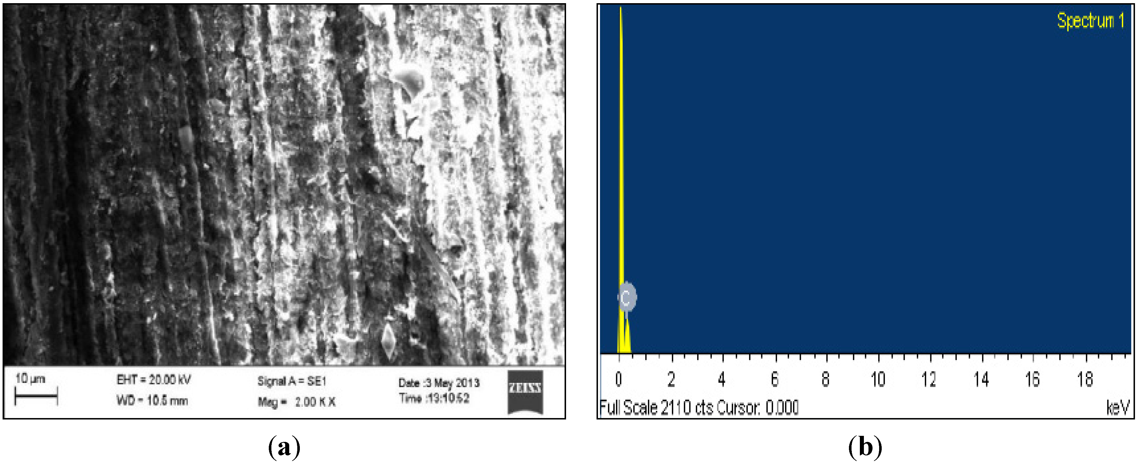
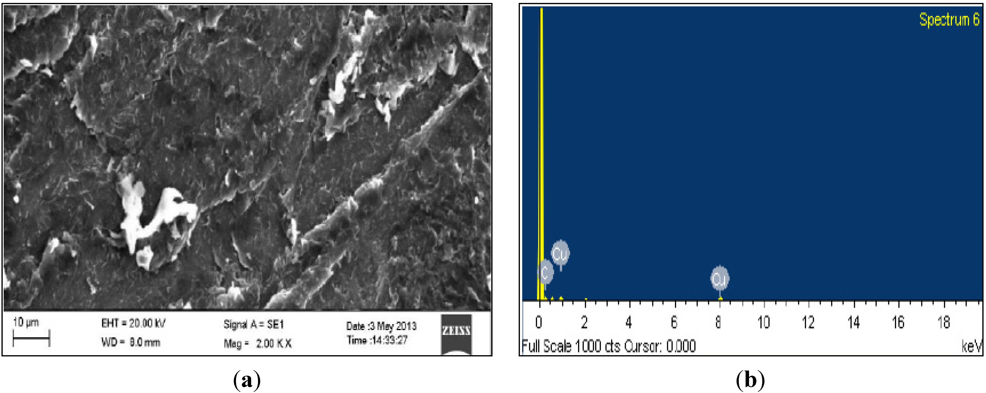
3.3. SEM/EDS Characterization

A ZEISS EVO- MA10 SEM scanning electron microscope (SEM, Carl Zeiss, Oberkochen, Germany) coupled with an energy dispersive X-ray spectrometer (EDS, Zeiss, Oberkochen, Germany) was used to examine the appearance and elemental composition of the Cu-deposited ABS surfaces.

4. Result and Discussion

4.1. Electrical Performance of Copper Deposited ABS Parts

Table 1 and Table 2 show the electrical performance of samples whose surfaces were prepared using Route 1 and Route 2, respectively. These readings are taken at room temperature after 1 h, 24 h and 48 h of deposition time. It is important to mention that conductivity is not obtained at all of the measured points; hence, the average resistance (R) and standard deviation (σ) have been calculated only for those points where the resistance value is obtained. Conductivity is obtained only for the HF and H2SO4 bath and not for the H3PO4 and CH3COOH bath for samples prepared through Route 1 (Table 1). For samples prepared through Route 2, except the CH3COOH bath, all of the acidic baths make the sample conductive (Table 2). For both of the individual routes, the best conductivity is obtained in the H2SO4 bath after 48 h of deposition time. However, it is to be noted that the resistance value through these routes is in MΩ).
Table 1. Electrical performance of samples prepared from Route 1 after electroless Cu deposition from different acidic baths.
Deposition Time (h)Acidic Bath
HFH2SO4H3PO4CH3COOH
R (MΩ)σR (MΩ)σR (MΩ)σR (MΩ)σ
1
240.120.020.110.03
480.110.010.090.01
“–” denotes that there is no conductivity.
Table 2. Electrical performance of samples prepared from Route 2 after electroless Cu deposition from different acidic baths.
Deposition Time (h)Acidic Bath
HFH2SO4H3PO4CH3COOH
R (MΩ)σR (MΩ)σR (MΩ)σR (MΩ)σ
1
244.871.012.150.613.070.52
484.150.562.100.392.950.55
“–” denotes that there is no conductivity.
To understand the difference in conductivity in each route and different acidic baths, the growth and distribution of Cu on different samples were studied using SEM (scanning electron microscope) images of all of the treated parts. The EDS (energy dispersive spectrometer) of Cu-deposited ABS samples were also performed for typical EDS spectra. As good conductivity was obtained after a 48-h deposition time, only SEM and EDS data at this particular time are presented in the next subsection.

4.2. SEM and EDS Characterization of Samples of Route 1

SEM and EDS image for the sample dipped in HF bath at room temperature for 48 h of deposition time is shown in the Figure 2. Cu deposition is not clearly visible in SEM. However, the EDS spectra show that the Cu peak is present in addition to some other elements. The presence of the copper peak and the height of copper peak dictate the presence of copper with weight percentage. The composition of Cu among these elements is 0.32%. The images for the sample dipped in the H2SO4 bath is presented in Figure 3. It consists of the SEM image and EDS spectra of the electroless deposited sample. Large Cu crystals can be clearly viewed in the SEM image. Elemental analysis shows 88.83% Cu is there in addition to the other element.
Figure 2. (a) SEM image and (b) EDS spectra of Cu electrolessly deposited on the sample whose surface is prepared through Route 1 in the HF bath.
Coatings 04 00574 g002
Figure 3. (a) SEM image and (b) EDS spectra of Cu electrolessly deposited on the sample whose surface is prepared through Route 1 in the H2SO4 bath.
Coatings 04 00574 g003
Figure 4 represents the SEM image and EDS spectra of the sample deposited in the H3PO4 bath for 48 h of deposition time. The SEM image has a very poor appearance with no visible copper. EDS spectra also make it clear that no copper is present. Figure 5 shows the SEM and EDS image for the sample dipped in the CH3COOH bath for 48 h of deposition time. The SEM image is very poor, with no Cu crystals at all. The EDS spectra of the sample are also shown in the figure.
Figure 4. (a) SEM image and (b) EDS spectra of Cu electrolessly deposited on the sample whose surface is prepared through Route 1 in the H3PO4 bath.
Coatings 04 00574 g004
Figure 5. (a) SEM image and (b) EDS spectra of Cu electrolessly deposited on the sample whose surface is prepared through Route 1 in the CH3COOH bath.
Coatings 04 00574 g005

4.3. SEM and EDS Characterization of Samples of Route 2

Figure 6 corresponds to the SEM and EDS images obtained after depositing the samples in the HF bath. Small Cu particles dispersed in the part can be seen in the SEM image. The EDS spectra as shown indicate a small Cu peak at 8 keV, indicating 100% Cu, at the point where the spectra are taken. Figure 7 presents the results for the sample deposited in the H2SO4 bath. The SEM image is presented, having charged white areas where Cu deposition is expected. EDS spectra correspond to 94% Cu and 6% C. Figure 8 depicts SEM and spectra for the sample deposited in the H3PO4 bath. The SEM image of the sample has a few Cu particles dispersed in the part. The EDS spectra correspond to 86% Cu, 11% O and 3% P. Finally, the sample deposited in the CH3COOH bath is presented in Figure 9. The SEM image has a very poor appearance with no clear sign of Cu deposition. The elemental composition also shows no copper percentage.
For both of the routes, the distribution obtained is poor. As the Cu gets deposited only at the site where catalyst palladium (Pd) and/or tin (Sn) colloid has been deposited by removing butadiene from the ABS part during the etching stage of surface preparation. The etching may not be able to create cavities throughout the part, which leads to non-uniform or localized deposition of Cu.
Figure 6. (a) SEM image and (b) EDS spectra of Cu electrolessly deposited on the sample whose surface is prepared through Route 2 in the HF bath.
Coatings 04 00574 g006
Figure 7. (a) SEM image and (b) EDS spectra of Cu electrolessly deposited on the sample whose surface is prepared through Route 2 in the H2SO4 bath.
Coatings 04 00574 g007
Figure 8. (a) SEM image and (b) EDS spectra of Cu electrolessly deposited on the sample whose surface is prepared through Route 2 in the H3PO4 bath.
Coatings 04 00574 g008
Figure 9. (a) SEM image and (b) EDS spectra of Cu electrolessly deposited on the sample whose surface is prepared through Route 2 in the CH3COOH bath.
Coatings 04 00574 g009

4.4. Adhesion Evaluation for ABS Parts

The adhesion evaluation of all of the ABS samples is done according to the scale defined by ASTM D 3359-02. All of the ABS test samples after the tape test show no flaking and yield results in a scale 4 or 5, meaning excellent adhesion strength, as only less than 5% of the deposited materials could be removed by the tape (Table 3).
Table 3. Adhesion performance assessment of electroless deposited Cu layers on ABS parts.
Deposition ConditionBath
HFH2SO4H3PO4CH3COOH
Scale5554

5. Conclusions

Metallization of ABS parts has been studied on flat surfaces. Two different routes were employed for preparing the ABS surface for achieving the metallization on them. These routes applied are:
  • Route 1: ABS parts prepared using chromic acid for etching.
  • Route 2: ABS parts prepared using H2SO4/H2O2 for etching.
After surface preparation using these two routes, Cu is deposited electrolessly using four different acidic baths. The acidic baths used are 5 wt% CuSO4 with 15 wt% of individual HF, H2SO4, H3PO4 and CH3COOH acids. Cu deposition in different acidic baths for both routes was presented with their electrical performance measurements, SEM images and EDS analyses in this study.
A better deposition of copper is observed through Route 1 when compared. Although Route 2 provides a conductivity value in the three baths, except CH3COOH, the sample prepared through Route 2 shows better conductivity in the HF and H2SO4 bath, though no conductivity in remaining acidic bath. It is also important to state that a varying amount of conductivity was obtained for different acidic baths used. The reason for the varying conductivity is due to the different size and non-uniform distribution of Cu in each route and in different acidic baths. Furthermore, an important observation is that the conductivity improves with the deposition time for the entire acidic bath showing conductivity. Furthermore, it can be observed that for both of the routes, the H2SO4 bath gives the best result with no conductivity for the CH3COOH bath. Hence, H2SO4 is the most effective acid used in this study. This is further validated with the SEM image and EDS spectra. Thus, it can be noted that the H2SO4 bath is the best suited for the electroless deposition of copper on ABS parts. Furthermore, from the above experimental work, it can be concluded that the CH3COOH bath is not suitable for electroless metallization.
Based on the current results, the development of a simpler and more cost-efficient Cu plating bath to further optimize the deposition conditions (the concentration of acids, deposition temperature and deposition time) is desired. Besides these, the lack of uniformity of Cu layers deposited under current conditions may become another focus of our future efforts.

Acknowledgements

All the experimental work is carried out in the Rapid Prototyping Lab of National Institute of foundry and forge technology and SEM/EDS images are taken at RDCIS, Ranchi. We also acknowledge the unanimous referees for their valuable comment in the preparation of this technical paper.

Author Contributions

The whole work is possible because of immense effort of both the authors Azhar equbal and Anoop kumar Sood. This work is very dedicatedly supervised by Anoop kumar Sood. The idea was taken from the literature but none of the literature has compared both the routes and the performance was not measured. Thus both the authors decided to compare them and tried to draw the conclusion. The individual idea was also implemented without confliction. Thus the work is made possible.

Conflicts of Interest

The authors declare no conflict of interest.

References

  1. Kuzmik, J.J.; Mallory, G.O.; Hajdu, J.B. Electroless Plating: Fundamentals and Applications; The American Electroplaters and Surface Finishers Society: Orlando, FL, USA, 1990. [Google Scholar]
  2. Mittal, K.L. Metallized Plastics Fundamental and Applied Aspects, 1st ed.; VSP BV: Utrecht, The Netherlands, 2001. [Google Scholar]
  3. Domenech, S.; Lima, E., Jr.; Drago, V.; Lima, J.; Borges, N.G., Jr.; Avila, A.; Soldi, V. Electroless plating of nickel-phosphorous on surface-modified poly(ethylene terephthalate) films. J. Appl. Surf. Sci. 2003, 220, 238–250. [Google Scholar] [CrossRef]
  4. Zhang, M.C.; Kang, E.T.; Neoh, K.G.; Tan, K.L. Electroless plating of copper and nickel on surface modified poly (tetrafluoroethylene) films. J. Electrochem. Soc. 2001, 148, 71–80. [Google Scholar] [CrossRef]
  5. Radulescu, F.; Miller, P.; Cunnane, L.; Harris, M.; Lam, H.; Bowers, C. Complete sputtering metallization for high-volume manufacturing. J. III Vs Rev. 2002, 15, 42–45. [Google Scholar]
  6. Griehl, S.; Muller, T.; Winkler, R. Thick metallization-layers on polymers through vacuum-technology. J. Surf. Coat. Technol. 2003, 169, 24–26. [Google Scholar] [CrossRef]
  7. Long, P.; Blackburn, M.; Watkins, J. Chemical fluid deposition: A hybrid technique for low temperature metallization. J. Adv. Mater. 2000, 12, 913–915. [Google Scholar] [CrossRef]
  8. De Bruyn, K.; van Stappen, M.; de Deurwaerder, H.; Rouxhet, L.; Celis, J.P. Study of pretreatment methods for vacuum metallization of plastics. J. Surf. Coat. Technol. 2003, 163–164, 710–715. [Google Scholar] [CrossRef]
  9. Hanna, F.; Hamid, A.; Aal, A. Controlling factors affecting the stability and rate of electroless copper plating. J. Mater. Lett. 2003, 58, 104–109. [Google Scholar] [CrossRef]
  10. Nicolas, D.; Pascu, M.; Vasile, C.; Poncin, F. Influence of the polymer pre-treatment before its electroless metallization. J. Surf. Coat. Technol. 2006, 200, 4257–4265. [Google Scholar] [CrossRef]
  11. Wang, X.; Li, N.; Li, Y. Effect of Pd ions in the chemical etching solution. J. Univ. Sci. Technol. 2007, 14, 286–289. [Google Scholar] [CrossRef]
  12. Dia, L.; Liua, B.; Songb, J.; Shanb, D.; Yangb, D. Effect of chemical etching on the Cu/Ni metallization of poly (ether ether ketone)/carbon fiber composites. J. Appl. Surf. Sci. 2011, 257, 4272–4277. [Google Scholar] [CrossRef]
  13. Sood, A.K.; Ohdar, R.K.; Mahapatra, S.S. Improving dimensional accuracy of Fused Deposition Modeling processed part using grey Taguchi method. J. Mater. Design 2009, 30, 4243–4252. [Google Scholar] [CrossRef]
  14. Sood, A.K.; Ohdar, R.K.; Mahapatra, S.S. Parametric appraisal of mechanical property of fused deposition modeling processed parts. J. Mater. Design 2010, 31, 287–295. [Google Scholar] [CrossRef]
  15. Lustraflex Material Safety Data Sheet; Leathertone Plastic Supply: Findlay, OH, USA, 2009.
  16. Charbonnier, M.; Romand, M. Polymer pretreatments for enhanced adhesion of metals deposited by the electroless process. Int. J. Adhes. Adhes. 2003, 23, 277–285. [Google Scholar] [CrossRef]
  17. Luan, B.; Yeung, M.; Wells, W.; Liu, X. Chemical surface preparation for metallization of stereolithography polymers. J. Appl. Surf. Sci. 2000, 156, 26–38. [Google Scholar] [CrossRef]
  18. Wang, G.-X.; Li, N.; Hu, H.-L.; Yu, Y.-C. Process of direct copper plating on ABS plastics. J. Appl. Surf. Sci. 2006, 253, 480–484. [Google Scholar] [CrossRef]
  19. Teixeira, L.A.C.; Santini, M.C. Surface conditioning of ABS for metallization without the use chromium baths. J. Mater. Process. Technol. 2005, 170, 37–41. [Google Scholar] [CrossRef]
  20. Shu, Z.; Wang, X. Environment-friendly Palladium free surface activation technics for ABS Surface. J. Appl. Surf. Sci. 2012, 258, 5328–5331. [Google Scholar] [CrossRef]
  21. Fritz, N.; Koo, H.; Wilson, Z.; Uzunlar, E.; Wen, Z.; Yeow, X.; Allen, S.; Kohl, P. Electroless deposition of copper on organic and inorganic substrates using a Sn/Ag catalyst. J. Electrochem. Soc. 2012, 159, 386–392. [Google Scholar]
  22. Wu, X.; Sha, W. Surface morphology of electroless copper deposits using different reducing agents, synthesis and reactivity in inorganic metal-organic and nano-metal chemistry. Taylor Francis 2008, 38, 292–296. [Google Scholar]
  23. Ono, S.; Naitoh, K.; Osaka, T. Initial propagation stage of direct copper plating on non-conducting substrates. J. Electrochem. Acta 1999, 44, 3697–3705. [Google Scholar] [CrossRef]
  24. Naruskevicius, L.; Tamasauskaite-Tamasiunaite, L.; Xieliene, A.; Jasulaitiene, V.A. Co-based surface activator for electroless copper deposition. J. Surf. Coat. Technol. 2012, 206, 2967–2971. [Google Scholar] [CrossRef]
  25. Kelly, J.; Mongey, K.; Gobil, Y.; Torres, J.; Kelly, P. Room temperature electroless plating copper seed layer process for damascene inter level metal structures. J. Microelectron. Eng. 2000, 50, 473–479. [Google Scholar] [CrossRef]
  26. Hong, S.; Shin, C.; Park, J. Palladium activation of TaNx barrier films for autocatalytic electroless copper deposition. J. Electrochem. Soc. 2002, 149, 85–88. [Google Scholar] [CrossRef]
  27. ASTM D3359–09 Standard Test Methods for Measuring Adhesion by Tape Test; American Society for Testing and Materials: West Conshohocken, PA, USA, 2010.

