Article

TiCl4 Barrier Process Engineering in Semiconductor Manufacturing

Macronix International Co. Ltd., Technology Development Center, No. 16, Li-Hsin Road, Science Park, Hsinchu 30078, Taiwan
*
Author to whom correspondence should be addressed.
Coatings 2016, 6(1), 2; https://doi.org/10.3390/coatings6010002
Submission received: 3 August 2015 / Revised: 25 December 2015 / Accepted: 7 January 2016 / Published: 12 January 2016
(This article belongs to the Special Issue Trends in Coatings and Surface Technology—Feature Papers)

Abstract

:
Titanium nitride (TiN) not only was utilized in the wear-resistant coatings industry but it was also adopted in barrier processes for semiconductor manufacturing. Barrier processes include the titanium (Ti) and TiN processes, which are commonly used as diffusion barriers in via/contact applications. However, engineers frequently struggle at the via/contact module in the beginning of every technology node. As devices shrink, barrier processes become more challenging to overcome the both the physical fill-in and electrical performance requirements of advanced small via/contact plugs. The aim of this paper is to investigate various chemical vapor deposition (CVD) TiCl4-based barrier processes to serve the application of advanced small via/contact plugs and the metal gate processes. The results demonstrate that the plasma-enhanced chemical vapor deposition (PECVD) TiCl4-based Ti process needs to select a feasible process temperature to avoid Si surface corrosion by high-temperature chloride flow. Conventional high step coverage (HSC) CVD TiCl4-based TiN processes give much better impurity performance than metal organic chemical vapor deposition (MOCVD) TiN. However, the higher chloride content in HSC film may degrade the long-term reliability of the device. Furthermore, it is evidenced that a sequential flow deposition (SFD) CVD TiCl4-based process with multiple cycles can give much less chloride content, resulting in faster erase speeds and lower erase levels than that of conventional HSC TiN.

1. Introduction

Titanium nitride (TiN) is widely used for wear-resistant coatings in the corrosion and surface treatment industry due to its hardness and high melting point [1]; moreover, it has been known to be an excellent contact for via diffusion barrier layers and metal gates in semiconductor manufacturing [2,3,4]. TiN also meets the requirements for improving the adhesion properties between tungsten chemical vapor deposition (W-CVD) and oxide. The formation of a titanium silicide (TiSix) contact with a TiN barrier is currently being used to prevent the WF6 from penetrating in the contact module, which then improves the adhesion performance by reacting to form a thin TiSix layer. Fluoride penetration through the TiN results in junction leakage and the formation of volcano defects by a reaction with the underlying Ti [5,6]. Conventionally, Ti/TiN films grown by physical vapor deposition (PVD) exhibit poor step coverage and therefore are not suitable for submicron-integrated devices. Continuous deposition by ion metal plasma (IMP) titanium deposition and the metal organic chemical vapor deposition (MOCVD) TiN technique with a precursor of tetrakis(dimethylamido)titanium (TDMAT) is widely utilized in 0.5 μm node technology and beyond because of its superior step coverage performance compared with PVD. However, the resistivity of as-deposited MOCVD TiN films is very high, mainly due to carbon impurities, and the high impurities of the metal organic compound will be a concern during the N2/H2 in situ plasma treatment after deposition [7,8]. As devices shrink, TiCl4-based plasma-enhanced chemical vapor deposition (PECVD) of Ti and chemical vapor deposition (CVD) of TiN is adopted as an alternative process solution due to its step coverage performance and fill-in capability in high-aspect-ratio, small, deep-contact processes. Unfortunately, the TiCl4-based Ti/TiN process temperature is higher than 600 °C, and it constrains their application at the contact level only [2,9,10]. Efforts to reduce the deposition temperature by different deposition process approaches are included with sequential flow deposition (SFD) [2], atmosphere pressure CVD (APCVD) [11], electron cyclotron resonance CVD (ECR-CVD) [12] and atomic layer deposition (ALD) [13], etc. Although the TiCl4-based TiN barrier process has a much lower impurity level than that of the MOCVD TiN process, remaining chloride impurities still have a deterioration in the long-term reliability of the device [14]. Ducroquet et al. proposed that CVD TiCl4-based TiN film acts as damascene gate electrode and shows excellent properties for metal-oxide-semiconductor (MOS) performances and gate oxide integrity, even on ultrathin gate oxide [15].
Furthermore, the W/TiN metal gate has been wildly applied in complementary metal-oxide-semiconductor (CMOS) devices when scaling into a 100 nm regime by virtue of its effective work function (EWF), low resistivity and fine diffusion barrier [16,17,18]. Variations on TiN properties have been reported for different deposition processes [16,17,18,19]. Some investigators proposed to modulate the composition of TiN to get different electrical characteristic, i.e., nitrogen-rich TiN exhibits more positive VFB shift with relatively thicker equivalent oxide thickness (EOT). By varying gas flow rates and TiN composition in PVD TiN, the VFB modulation range is about 120 mV and the EOT of HfO2 is reduced by 0.4–0.5 nm [18]. Vitale et al. address that the EWF of the TiN metal gate is tunable within the range of 4.30–4.65 eV by adjusting the PVD process parameters [19]. Furthermore, thinner TiN thickness improves the variation in EFW and reduces gate dielectric charge. PVD TiN has better film properties relative to MOCVD TiN due to higher impurities in the MOCVD TiN film [16]. However, there is a significant charge-arising phenomenon on gate dielectrics by the PVD TiN process. A CVD TiCl4-based TiN process that is processed by TiCl4 and NH3 precursors with less impurity is proposed by Nakajima, which has lower gate leakage and better flat-band voltage performance [17].
Based on the reported EWF values with different TiN metal gate processes showing large variation, the TiCl4-based CVD TiN is the one of good candidates for metal gate engineering. In the meantime, TiCl4-based PECVD Ti and CVD TiN can serve with advanced via/contact fill-in application. The aim of this paper is to optimize the TiCl4-based Ti/TiN processes and investigate the root cause of contact electrical failure. Furthermore, the impurities of different TiN processes and their post-thermal annealing performances are studied for improving the film quality and preventing further degradation, and the erase level performance of different CVD TiN metal gate processes is also included in this study.

2. Experimental Section

The 300 mm Si wafer integrated with different technology nodes devices were used for TiCl4-based Ti/TiN processes verification. TiCl4-based Ti films were deposited using PECVD process by reaction of TiCl4 and H2 at 550, 600, and 650 °C, respectively. Subsequently, TiN films were deposited on Ti films using different CVD TiCl4-based process approaches high step coverage (HSC) and SFD with the reaction gases of TiCl4 and NH3. The heat treatment was performed by rapid thermal processing (RTP) after Ti/TiN deposition. In addition, for the comparison, the via/contact holes of various technology nodes were deposited with PVD Ti/TiN or IMP Ti /MOCVD TiN and then thermally annealed to form a TiSix with low contact resistance. The fill-in performance of via/contact plugs by different approaches and its corresponding microstructure were evaluated by transmission electron microscopy (TEM) cross-section. Impurities analysis was probed by secondary ion mass spectrometry (SIMS) profile and the non-contact CV interface trap density (Dit) measurement item.

3. Results and Discussion

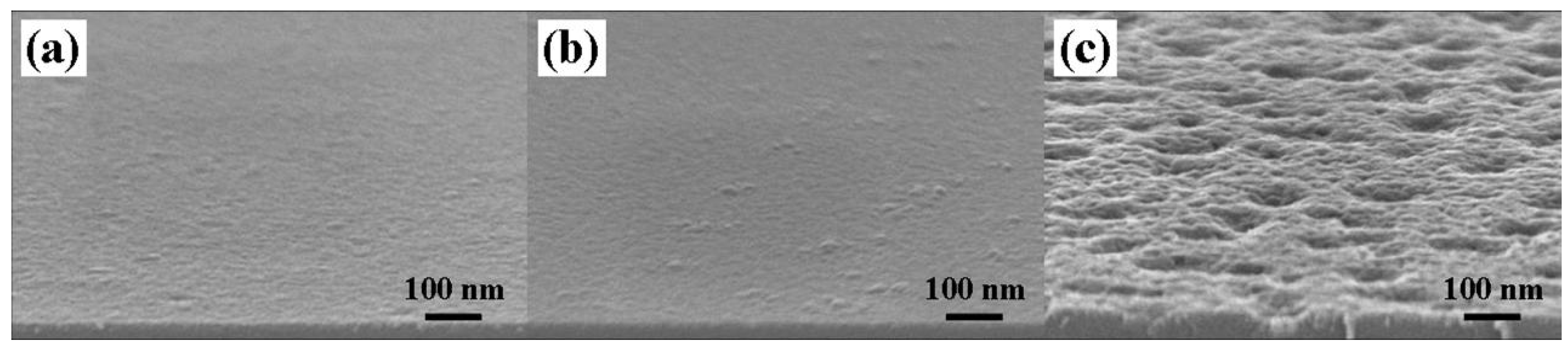
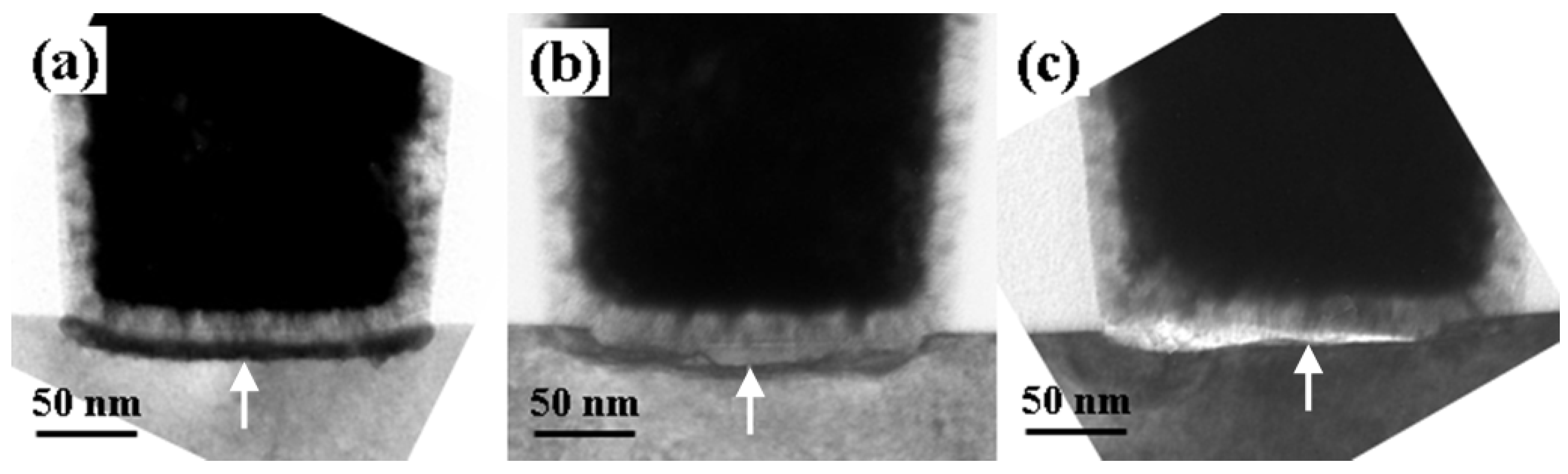
3.1. PECVD TiCl4-Based Ti Process

PECVD of Ti using TiCl4 has been investigated as an alternative process solution due to its excellent bottom coverage and capability of in-situ silicide formation on Si substrate under high deposition temperature. However, relatively high temperature deposition may cause Si surface corrosion and then affect the performance of the devices. Figure 1 demonstrates the silicon surface profile after processing with PECVD TiCl4-based Ti under different process temperatures. Compared with the wavy and concave surface at 650 °C, surface roughness can be improved as the process temperature decreases, resulting in a smoother TiN cap, as shown in Figure 2. In addition, PECVD TiCl4-based Ti at the low temperature of 550 °C can give better TiSix formation relative to that at 650 °C processing with contact open and discontinuous effect (Figure 3). The defect on the Si surface is probably corroded by chloride flow at high temperatures. Figure 4 shows the contact resistance performance with different PECVD TiCl4-based Ti process temperatures. Serious tail bit is observed in the high-temperature 650 °C PECVD Ti process. Therefore, a feasible PECVD TiCl4-based Ti process temperature plays an important factor in the contact resistance and performance.
Figure 1. SEM images of PECVD TiCl4-based Ti films on Si surface at process temperatures of (a) 550 °C; (b) 600 °C; (c) 650 °C.
Coatings 06 00002 g001
Figure 2. Cross-sectional TEM images of PECVD TiCl4-based Ti covered with same TiN films at (a) 550 °C; (b) 600 °C; (c) 650 °C.
Coatings 06 00002 g002
Figure 3. Contact bottom profiles for TiSix formation at (a) 550 °C; (b) 600 °C; (c) 650 °C. The arrowhead represents the TiSix formation quality.
Coatings 06 00002 g003
Figure 4. Cumulative probability plot of contact resistance for PECVD TiCl4-based Ti at different process temperatures.
Coatings 06 00002 g004

3.2. Impurity Analysis of TiN

The Dit item is implemented to monitor the different TiN impurities from the diffusion behavior after RTP on thermal oxide. As shown in Figure 5, the Dit value was almost consistent in each sample before TiN deposition or post-thermal annealing. However, 450 °C MOCVD TiN four × 50 (50 Å deposition four times) impurity is activated by RTP at 600 °C which shows much higher Dit than that of TiCl4-based TiN. The TiCl4-based TiN Dit item shows no change, even after the RTP process. Furthermore, we also found that the device cell near the contact with IMP Ti and MOCVD TiN had a worse charge loss reliability issue than that of the cell far away from the contact. Therefore, impurities can diffuse out from MOCVD TiN and then impact the cell performance.
Figure 5. MOCVD TiN’s impurity is activated by RTP thermal which shows much higher Dit than that of TiCl4-based TiN.
Coatings 06 00002 g005
Figure 6 illustrates the precursor flow steps of three different deposition methodologies. Conventional HSC TiN is deposited by CVD with TiCl4 flow and NH3 flow and is subsequently treated with high NH3 flow for removal of the chloride element content, as shown in Figure 6a. As for the SFD TiN process, it is repeated with HSC steps and shorter deposition time with multiple cycles. Therefore, it can remain a lower chloride content in SFD using multiple treatments with the same thickness and process temperature. Figure 6c shows the precursor flow steps during the ALD TiCl4-based TiN process, which is similar to the SFD TiN process but the TiCl4 flow and NH3 flow are deposited separately.
Figure 6. Schematic diagrams of the precursor flow steps of (a) conventional HSC; (b) SFD; (c) ALD TiN deposition methodologies.
Coatings 06 00002 g006
HSC and SFD are adopted together to verify the chloride contents and the chlorine content by SIMS is normalized and summarized in Table 1. It indicates that normalized chloride of standard condition HSC CVD TiN film (designated as case A) is 236.28, and the chlorine content in HSC is 2.4 times higher than the SFD-process TiN deposition (designated as case B). As compared to the standard condition of conventional HSC TiN, the SFD process with the multi-cycle deposition function has the benefit of reduce the chlorine concentration.
Table 1. Normalized chlorine concentration in TiN films by SIMS analysis for different TiN cases.
CaseTiN TypeCycle CountProcess TemperatureNormalized Cl Concentration
AConventional HSCNASTD236.28
BSFDMultiSTD100

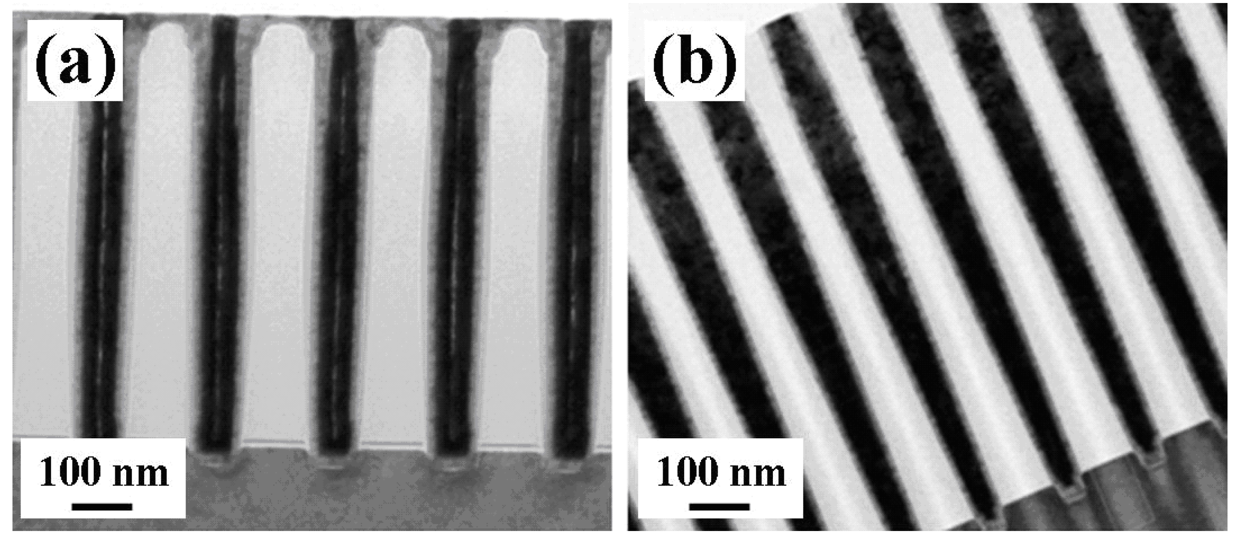
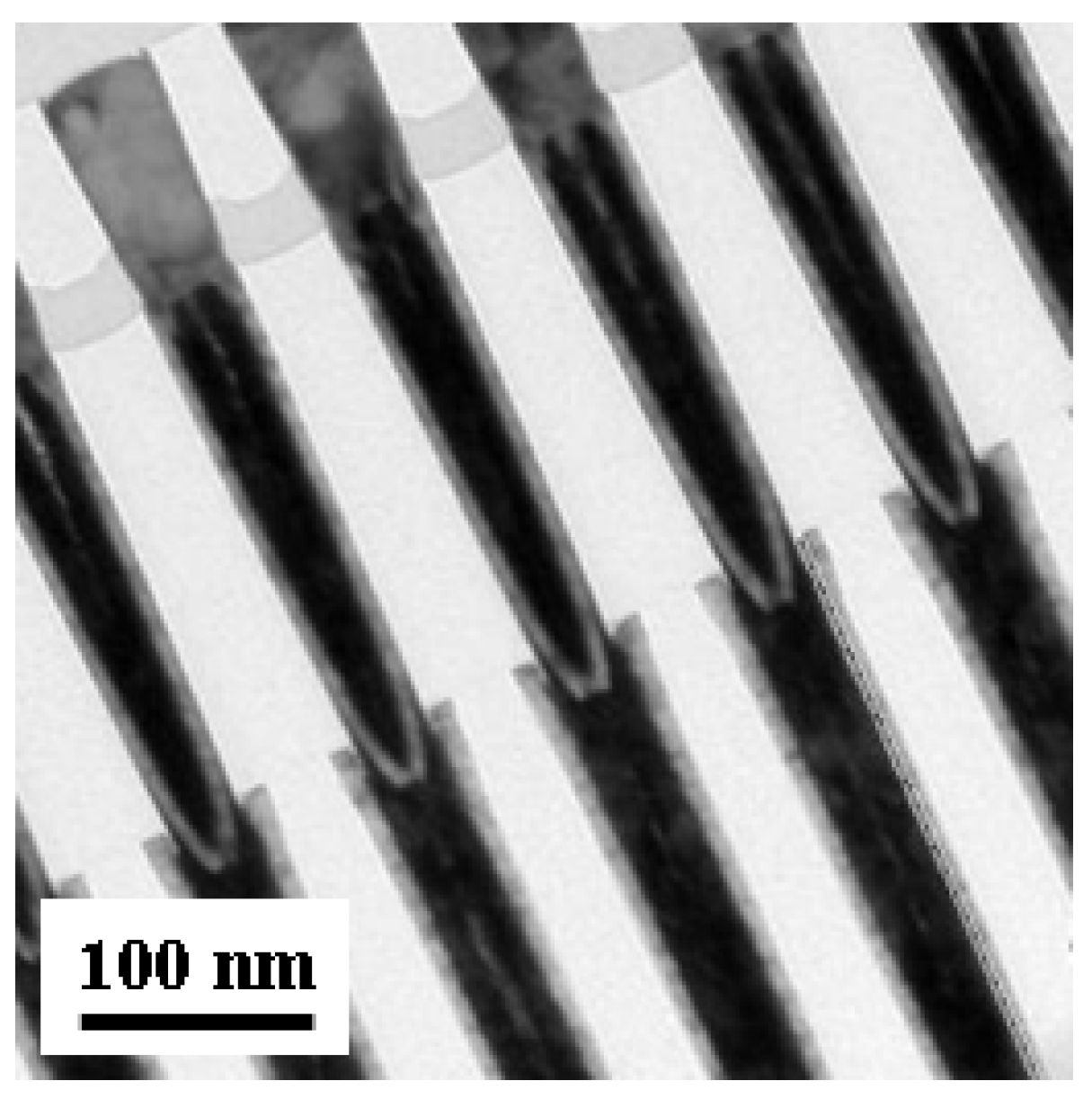
3.3. Excellent Step Coverage Requirement for High Aspect Ratio Deep Contact

As discussed previously, the excellent step coverage requirement for high-aspect-ratio applications such as deep contacts (>6:1) drives the development of CVD TiN. Figure 7a shows the IMP Ti with the MOCVD TiN fill-in step coverage performance, and it indicates that the overhang of the barrier is worse, and it needs to use a funnel-like profile for keeping the fill-in performance of the W-CVD process. On the contrary, Figure 7b demonstrates a well filled-in deep contact with an aspect ratio of 12:1 under a 12 kÅ inter-layer dielectric (ILD) bowing profile by using SFD TiCl4-based TiN. Furthermore, the low temperature SFD TiCl4-based TiN process can also be served with the small via step-coverage issue for protecting the W-CVD WF6 precursor penetration and improving the adhesion between the inter-metal dielectric (IMD), as shown in Figure 8. Based on these phenomena, it manifests that the CVD TiCl4-based TiN can not only be implemented in advanced small via applications but can also be adopted in high-aspect-ratio deep contacts with low temperature, high conformity and low resistance.
Figure 7. TEM images of fill-in performance on special funnel-like profile. (a) MOCVD TiN; (b) High aspect ratio of 12:1 deep contact with SFD TiN barrier.
Coatings 06 00002 g007
Figure 8. TEM image of plug performance in advanced small via application based on CVD TiCl4-based TiN.
Coatings 06 00002 g008

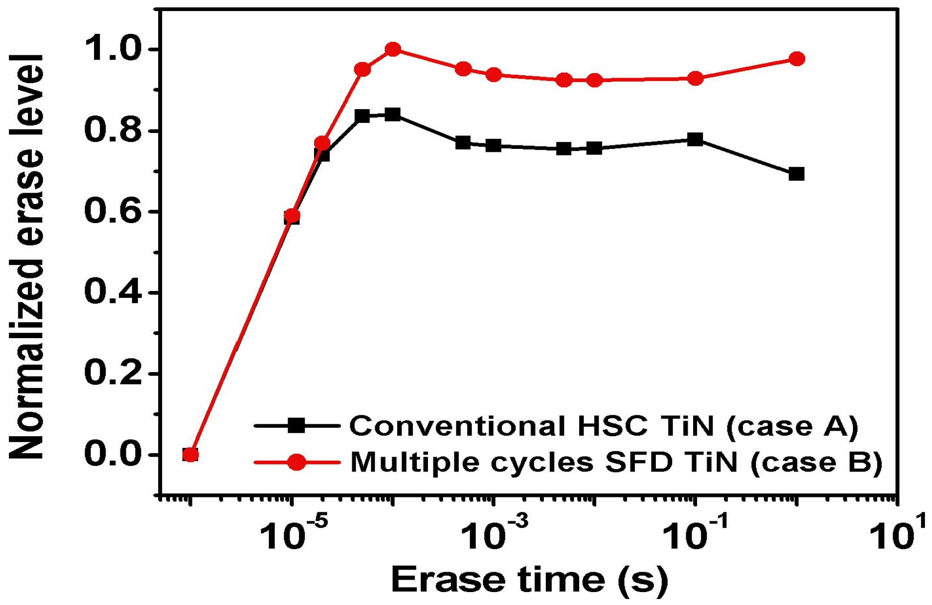
3.4. Erase Performance Improvement by TiN Metal Gate

Figure 9 shows the EOT distribution characteristics of various TiN metal gates. In contrast to the device with the conventional HSC TiN gate (case A), the average EOT can decrease from 169.3 Å to 167.4 Å by using the SFD TiN gate (case B), and the HSC TiN has a larger deviation. The trend of EOT characteristics matches with the SIMS analysis results of chloride concentration. Higher cycle numbers of the SFD process will get thinner EOT due to less chloride being incorporated into the oxide.
Figure 9. Distribution characteristic of equivalent oxide thickness in devices with different TiN gates.
Coatings 06 00002 g009
The characteristics of the device erase curve plot by erase time versus normalized erase level for HSC and SFD TiN metal gates is shown in Figure 10. The erase performances of the two TiN gates are comparable at the initial stage, but exhibit significant differences after the erase time of 10−5 s. The erase performance of conventional HSC TiN (case A) shows the lower erase speed and smaller erase level (80%); if it replaces the TiN gate in the SFD process (case B), the erase speed becomes faster and the erase level increases up to 100% at an erase time of 10−4 s. The erase speed and erase level show improvement by adopting the SFD TiN gate. It demonstrates that the higher cycle numbers in the SFD process with the same TiN thickness will have a lower chloride concentration due to more ammonia flow steps to neutralize the chloride contents in the bulk film, as revealed in Equations (1) and (2) below.
Figure 10. Normalized erase level change of devices for conventional FDC and GETiN gates.
Coatings 06 00002 g010
TiCl4 + NH3 → TiN + HCl or Ti(NH2)xCly + HCl
Ti(NH2)xCly + NH3 → TiN + HCl
In view of the results in Figure 9 and Figure 10, it is proposed that the erase level of the metal gate is highly correlative to the chloride concentration of the TiCl4-based TiN processes. Therefore, the electrical characteristics of multiple-cycle SFD TiN films get better erase levels than that of the conventional HSC ones. These results are consistent with Park et al. who proposed results that the reliability degradation is partially attributed to chloride in the TiCl4 precursor of the TiN metal gate [14].

4. Conclusions

Various TiN barrier processes are utilized widely for via/contact modules in semiconductor manufacturing. As design rules shrink, PVD TiN suffers step coverage and charging issues; MOCVD TiN struggles with high impurities and high resistance shortcomings. TiCl4-based HSC and multiple-cycle SFD CVD TiN approaches provide an alternative solution for next-generation advanced small via and deep contact applications. Furthermore, low chloride TiN processes, i.e., multiple-cycle SFD TiN, can achieve better erase levels of metal gates than that of conventional HSC.

Author Contributions

T.L., K.-C.C. and T.-H.Y. conceived and designed the experiments; T.L., Y.-K.H., and Y.-T.H. performed the experiments; T.L., and L.-W.Y. analyzed the data and performed the microstructure analysis; T.L. and Y.-K.H. wrote the paper.

Conflicts of Interest

The authors declare no conflict of interest.

References

  1. Santecchia, E.; Hamouda, A.M.S.; Musharavati, F.; Zalnezhad, E.; Cabibbo, M.; Spigarelli, S. Wear resistance investigation of titanium nitride-based coatings. Ceram. Int. 2015, 41, 10349–10379. [Google Scholar] [CrossRef]
  2. Cheng, M.-D.; Luoh, T.; Su, C.-T.; Yang, T.-H.; Chen, K.-C.; Lu, C.-Y. Improvement of the properties and electrical performance on TiCl4-based TiN film using sequential flow chemical vapor deposition process. Thin Solid Films 2010, 518, 2285–2289. [Google Scholar] [CrossRef]
  3. Liu, P.-T.; Chang, T.-C.; Hu, J.C.; Yang, Y.L.; Szea, S.M. Reliability of multistacked chemical vapor deposited Ti/TiN structure as the diffusion barrier in ultra large scale integrated metallization. J. Electrochem. Soc. 2000, 147, 368–372. [Google Scholar] [CrossRef]
  4. Shin, Y.-H.; Shimogaki, Y. Diffusion barrier property of TiN and TiN/Al/TiN films deposited with FMCVD for Cu interconnection in ULSI. Sci. Technol. Adv. Mater. 2004, 5, 399–405. [Google Scholar] [CrossRef]
  5. Sidhwa, A.; Spinner, C.; Gandy, T.; Brown, W.; Ang, S.; Naseem, H.; Ulrich, R. Evaluation of contact and via step coverage using a novel two-step titanium nitride barrier deposition process. MRS Proc. 2002, 716. [Google Scholar] [CrossRef]
  6. Prikh, S.; Akselrod, L.; Gardner, J.; Armstrong, K.; Parekh, N. TiN barrier integrity and volcano formation in W-plug applications. Thin Solid Films 1998, 320, 26–30. [Google Scholar] [CrossRef]
  7. Asinovsky, L.; Frisa, L.E. Characterization of PVD TiN uniformity. Thin Solid Films 1998, 313–314, 303–307. [Google Scholar] [CrossRef]
  8. Wu, C.M.; Wang, M.Y.; Shue, S.L.; Yu, C.H.; Liang, M.S. Integration of CVD W on MOCVD TiN. In Proceedings of the IEEE International Symposium on VLSI technology, System and Applications, Hsinchu, Taiwan, 18–20 April 2001.
  9. Huang, T.-Y.; Liang, W.-P.; Su, K.-H.; Wu, C.-R.; Lin, Y.-C.; Satoshi, W.; Lin, J.P. Effects of TiCl4-based PECVD-Ti/CVD-TiN barrier layers on the BF2-doped Si for contact plug technology. ECS Trans. 2007, 6, 15–20. [Google Scholar]
  10. Luoh, T.; Cheng, M.D.; Yeh, W.; Su, C.-T.; Yang, T.-H.; Chen, K.-C.; Ku, J.; Lu, C.-Y. Temperature and RF-plasma power effect on TiCl4 PECVD-Ti process for 0.1 m contact size and beyond. In Proceedings of the SEMICON Taiwan 2006, Taipei, Taiwan, 11–13 September 2006.
  11. Musher, J.N.; Gordon, R.G. Low-temperature CVD TiN as a diffusion barrier between gold and silicon. J. Electron. Mater. 1991, 20, 1105–1107. [Google Scholar] [CrossRef]
  12. Akahori, T.; Tanihara, A.; Yano, M. Preparation of TiN films by electron cyclotron resonance plasma chemical vapor deposition. Jpn. J. Appl. Phys. 1991, 30, 3558–3561. [Google Scholar] [CrossRef]
  13. Kim, Y.-S.; Jeon, H.; Kim, Y.D. Atomic-layer chemical-vapor-deposition of TiN thin films on Si(100) and Si(111). J. Korean Phys. Soc. 2000, 37, 1045–1050. [Google Scholar]
  14. Park, D.-G.; Kim, T.-K. Effects of fluorine and chlorine on the gate oxide integrity of W/TiN/SiO2/Si metal-oxide-semiconductor structure. Thin Solid Films 2005, 483, 232–238. [Google Scholar] [CrossRef]
  15. Ducroquet, F.; Achard, H.; Coudert, F.; Previtali, B.; Lugand, J.-F.; Ulmer, L.; Farjot, T.; Gobil, Y.; Heitzmann, M.; Tedesco, S.; et al. Full CMP integration of CVD TiN damascene sub-0.1 um metal gate devices for ULSI applications. IEEE Trans. Electron Devices 2001, 48, 1816–1821. [Google Scholar] [CrossRef]
  16. Yang, H.; Brown, G.A.; Hu, J.C.; Lu, J.P.; Kraft, R.; Rotondaro, A.L.P.; Hattangady, S.; Chen, I.-C.; Luttmer, J.D.; Chapman, R.A.; et al. A comparison of TiN processes for CVD W/TiN gate electrode on 3 nm gate oxide. IEDM 1997, 459–462. [Google Scholar]
  17. Nakajima, K.; Akasaki, Y.; Kaneko, M.; Tamaoki, M.; Yamada, Y.; Shimizu, T.; Ozawa, Y.; Suguro, K. Work function controlled metal gate electrode on ultrathin gate insulator. VLSI Tech. Dig. 1999, 96–97. [Google Scholar]
  18. Lee, S.-H.; Choi, R.; Choi, C. Effects of composition and thickness of TiN metal gate on the equivalent oxide thickness and flat-band voltage in metal oxide semiconductor devices. Microelectron. Eng. 2013, 109, 160–162. [Google Scholar] [CrossRef]
  19. Vitale, S.A.; Kedzierski, J.; Healey, P.; Wyatt, P.W.; Keast, C.L. Work-function-tuned TiN metal gate FDSOI transistors for subthreshold operation. IEEE Trans. Electron Devices 2011, 58, 419–426. [Google Scholar] [CrossRef]

