Communication

Cylindrical Three-Dimensional Porous Anodic Alumina Networks

by
Pedro M. Resende
,
Ruy Sanz
,
Alejandra Ruiz-de Clavijo
,
Olga Caballero-Calero
* and
Marisol Martin-Gonzalez
Instituto de Microelectrónica de Madrid (IMM-CSIC), Calle de Isaac Newton 8, Tres Cantos, 28760 Madrid, Spain
*
Author to whom correspondence should be addressed.
These authors contributed equally to this work.
Coatings 2016, 6(4), 59; https://doi.org/10.3390/coatings6040059
Submission received: 28 September 2016 / Revised: 28 October 2016 / Accepted: 2 November 2016 / Published: 9 November 2016
(This article belongs to the Special Issue Advances in Coatings Characterization)

Abstract

:
The synthesis of a conformal three-dimensional nanostructure based on porous anodic alumina with transversal nanopores on wires is herein presented. The resulting three-dimensional network exhibits the same nanostructure as that obtained on planar geometries, but with a macroscopic cylindrical geometry. The morphological analysis of the nanostructure revealed the effects of the initial defects on the aluminum surface and the mechanical strains on the integrity of the three-dimensional network. The results evidence the feasibility of obtaining 3D porous anodic alumina on non-planar aluminum substrates.

1. Introduction

Porous anodic alumina (PAA) is a well known and versatile self-ordered nanosystem synthesized by a two-step anodization process [1]. Standard PAAs are composed of amorphous Al2O3 containing impurities coming from the electrolyte. They present a hexagonal close-packed arrangement of pores that grow perpendicular to the aluminum seed layer. The diameter and the distance between pores can be tuned [2,3], under certain limits, employing different synthesis conditions during the two necessary steps of anodization, with additional chemical etchings to enlarge the pores after the double anodization process. This tunable morphology and the non-demanding equipment for the synthesis of PAA have boosted the inclusion of PAA as a common base material in many nanotechnology research groups. In fact, for more than 20 years, PAA has been employed in a wide field of applications [4], ranging from templates for the growing of diverse nanostructures to nanowires and anti-dots [5] or to scaffold for devices and sensors [6]. Recently, our group developed a method to synthesize a three-dimensional (3D) network of PAA, in sulfuric acid electrolyte [7]. This new approach is based on the application of pulsed potentiostatic anodization [8,9]. Briefly, in this method, the second anodization step is performed under standard mild anodization conditions (25 V) with the addition of periodic pulses within the hard anodization regime (33 V, for 2 s) and limiting the electrical current density to avoid electrical breakdowns. The alumina generated under hard anodization regimes, in this case during the pulses, presents higher etching rates than that obtained under a mild anodization regime [8]. Thus, after acid etching, a 3D nanostructured network is obtained. The 3D network consists of arrays of hexagonal parallel nanopores connected by transversal nanochannels, in which the distance between transversal nanochannels is tunable by the periods between hard anodization pulses.
In most cases, PAAs are synthesized on planar Al foils. Nevertheless, anodization is an electrochemical process able to obtain conformal nanostructured coatings. Among the non-planar geometries, anodic nanostructures based on Al and Ti are generated on macroscopic cylindrical shapes, e.g., wires and tubes [10,11,12,13,14,15,16,17]. These cylindrical geometries have received the attention of several researchers due to their possible advantageous integration in fluidic devices such as pipes and filters. The possibility of combining a 3D nanostructured network as a conformal coating with a non-planar geometry might open new possibilities for functional nanostructures. In this work, we present for the first time the synthesis and morphological characterization of three-dimensional cylindrical porous anodic alumina (3D-CPAA) synthesized on Al wires.

2. Materials and Methods
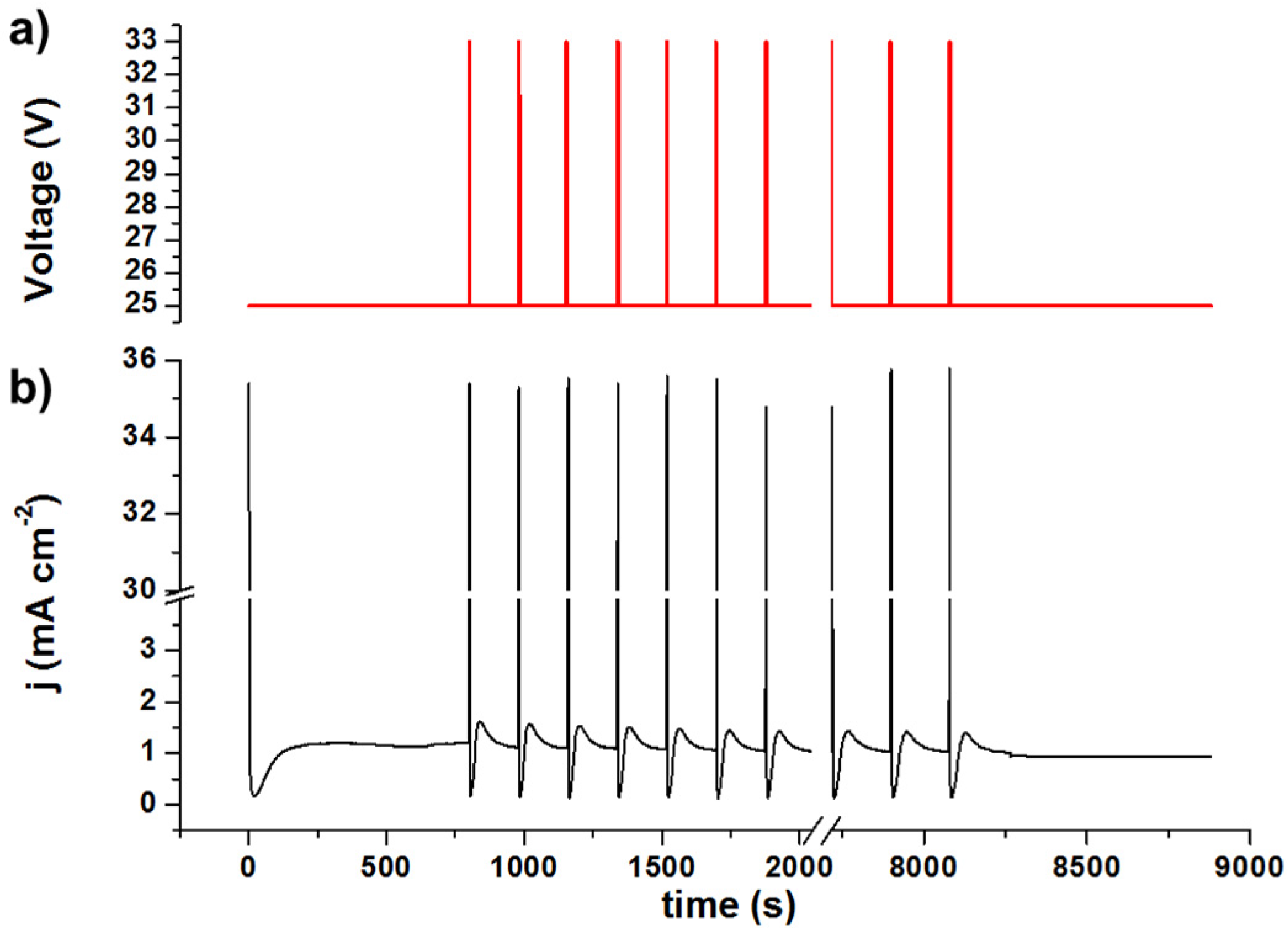
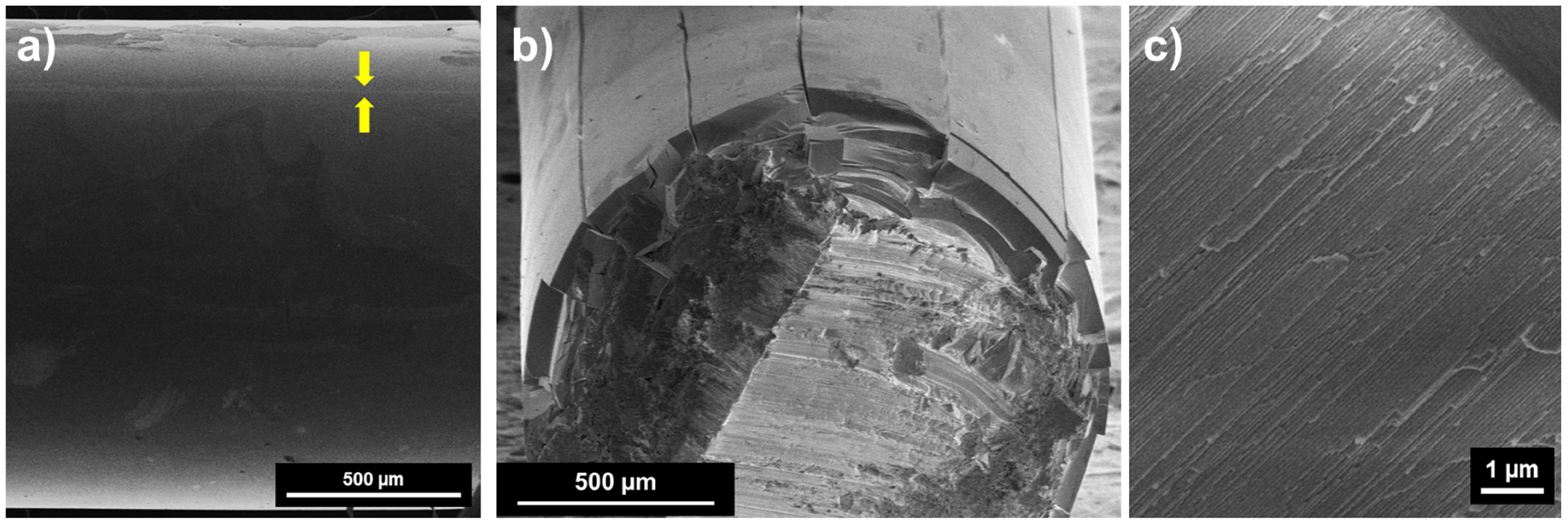
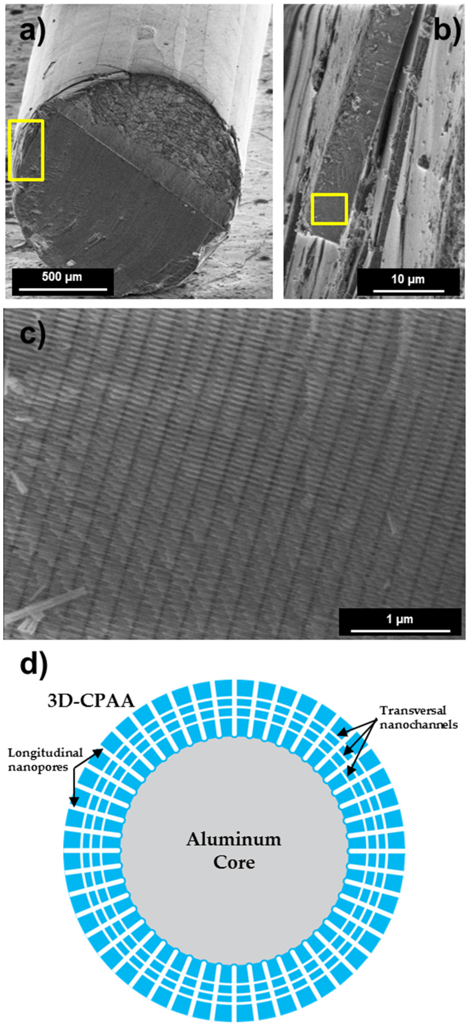
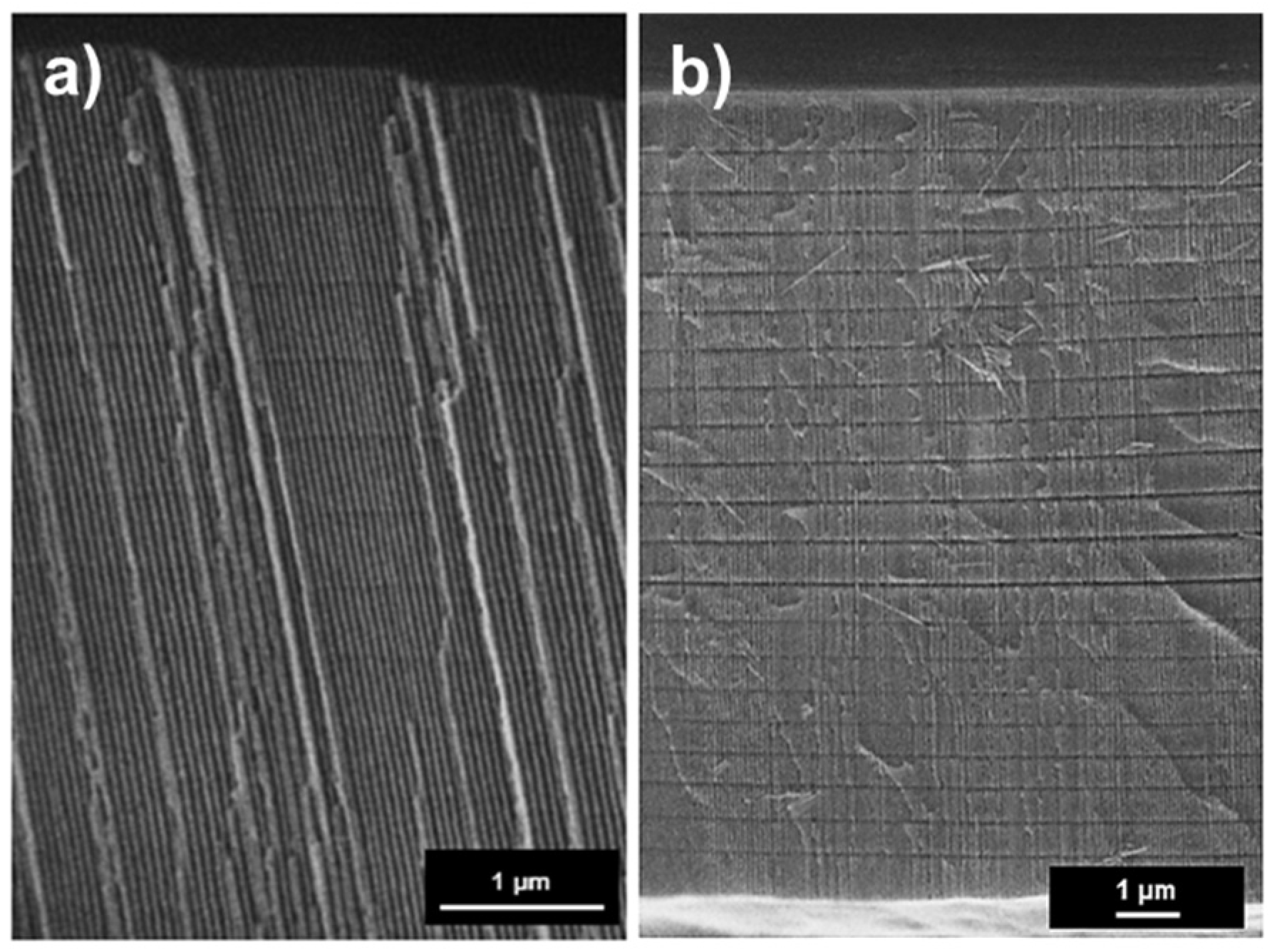
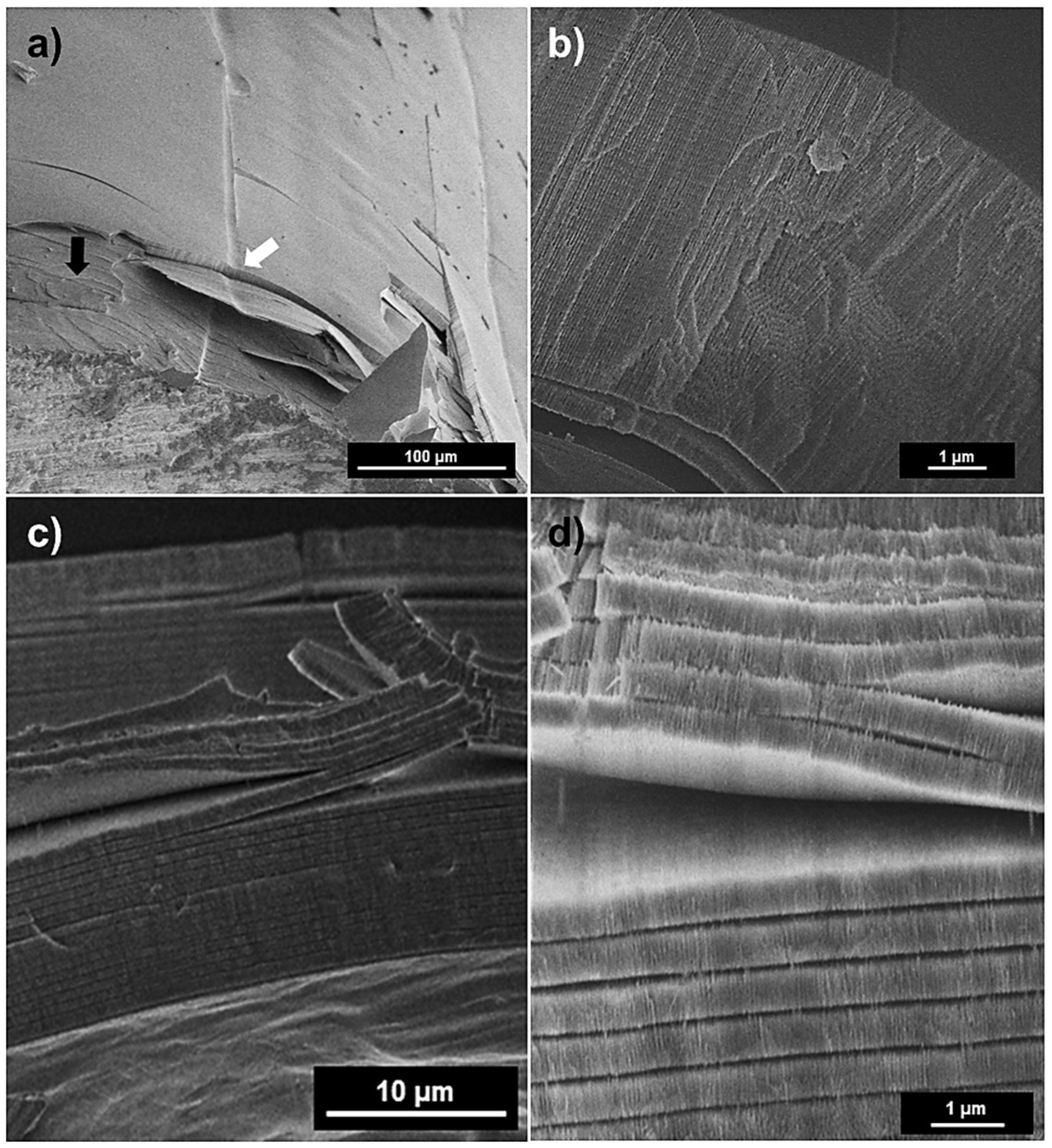
The employed process of obtaining 3D-CPAA is based on the combination of methods to obtain 3D-PAA and CPAA [7,11], adapted to the cylindrical geometry of the samples. Al wires (99.999 wt.%), 1.5 mm in diameter (Advent), were first cleaned with acetone, isopropanol, and, finally, ethanol under ultrasound. After cleaning, wires were electropolished in an ethanol and perchloric acid solution (75:25) at 20 V for 1 min to reduce the roughness of the Al surface. An initial anodization process was performed using sulfuric acid (0.3 M, Sigma-Aldrich, Steinheim, Germany) as an electrolyte at 1 °C and 25 V. The counter electrode was a platinum net. The tip and part of the surface of the wires were covered with standard Parafilm® films (Bemis Inc., Neenah, WI, USA) in order to avoid electrical breakdowns and to limit the exposed anodized surface of the wires. After the first anodization over 24 h, the oxide layer was dissolved by a mixture of chromic oxide (1.8 g) and phosphoric acid (7.1 g, 85 wt.%, both reagent grade Sigma-Aldrich) per 100 mL of deionized water for 24 h at room temperature. Then, the diameters of the employed wires were measured again in order to limit the current density. The second anodization process was carried out under the same anodization conditions. However, in the second anodization process, the voltage profiles included 2 s pulses of 33 V with an electrical current density limitation of 36 mA·cm−2. In addition, 800 s periods of constant 25 V were applied at the beginning and the end of these second anodization processes. Three different profiles were applied for three types of samples, each differing on the elapsed time between applied pulses: 180, 360, and 540 s. We will refer to the type of samples by the time periods of the second anodization (Table 1).
The electrical current was monitored for each sample by a computer connected multimeter with a 1 s sampling rate. The voltage anodization profile and an example of the measured current density in the S180 type sample are shown in Figure 1. Please note that a constant wire area is assumed for the electrical current density.
After these pulsed anodization processes, an acid etching process was performed for each sample for 23 min in a 5 wt.% phosphoric acid solution (85%, Prolabo, Briare le Canal, France) in order to generate the transversal nanochannels. Longer periods of etching were applied in order to observe the evolution of the nanostructure. The structural characterization of the obtained nanostructures was performed via high-resolution scanning electron microscopy (HRSEM, FEI Verios 460, Eindhoven, The Netherlands). Cross-sectional images of the samples were prepared via direct mechanical cuts.

3. Results

The as-received Al wires presented as longitudinal die lines, which are longitudinal lines produced by pulling the Al rod through a drawing die process [18]. These die lines remained even after the electropolishing process (Figure 2). The average diameter of the wires after electropolishing was 1.45 mm. The first anodization process generated an 80-µm-thick CPAA with parallel nanopores radially distributed around the core of the Al wire (see Figure 1).
These CPAA presented radial nanopores that were 35 nm in diameter and had an interpore distance of 65 nm. These values are in agreement with those obtained for planar PAA. No signals of partial detachment of the CPAA during the anodization process were observed. The HRSEM images revealed longitudinal cracks along the CPAA surface.
After the dissolution of that first CPAA in the chromic and phosphoric acid solution, the second anodization (pulsed) processes were performed. The registered density of the current of the samples during the second anodization presented the same behavior of those observed for the synthesis of 3D-PAA [7] (see an example in Figure 1). All those second anodizations resulted in ordered CPAA around the Al wires. The porous structure of these CPAA was similar to those obtained in the first anodization. The coverage was also kept after the etching in phosphoric acid to generate the transversal nanochannels, as is shown in Figure 3.
As a result of this etching, the transversal nanochannels were generated, and the average pore diameter was enlarged up to 60 nm. The obtained nanostructures presented longitudinal nanopores perpendicular to the Al surface, i.e., radially distributed around the Al core. The transversal nanochannels were perpendicular to the nanopores, i.e., parallel to the surface of the Al core. The samples synthesized by different periods of pulses exhibited different distances between transversal nanochannels. The pulse periods of 180, 360, and 540 s resulted in 250 ± 10, 482 ± 10, and 635 ± 15 nm distances between transversal nanochannels, respectively. Anodization periods of 800 s at the beginning and at the end of the pulsed anodization generated 880 ± 30 nm thick layers (see Figure 3d and Figure 4).
Cracks along the longitudinal axis also appeared on the surfaces; however, in these cases, the cracks are shallow compared to those observed in the first anodization (see Figure 5a,b). However, this type of defect modifies the ordering of the nanopores (Figure 5b). The mechanical cut applied to observe the cross section also induced the breakage of the 3D-CPAA in the form of terraces along the planes formed by the transversal nanochannels in some samples (see an example in Figure 5a). If longer etching periods in phosphoric acid are applied, i.e., >23’, an over-etching of the transversal nanochannels occurs. Thus, terraces start to detach before the complete dissolution of the radial nanopores. Therefore, very thin cylindrical porous alumina nanotubes can be generated. Some examples are presented in Figure 5c,d.

4. Discussion

The obtained results from the adaptation of the methodology to obtain 3D-PAA on flat Al foils to Al wires resulted successfully in 3D-CPAA. The generated 3D-CPAA displayed similar 3D networks to those generated in 3D-PAA, but with cylindrical macroscopic shapes. In fact, transversal nanochannels distribute perpendicularly to the now radial nanopores and parallel to the circular section of the wire. The size and interpore distance of the longitudinal (radial) nanopores are the same, and the distances between transversal nanochannels in both networks are in good agreement. The obtained distances between transversal nanochannels as a function of mild anodization periods fit a linear growing rate of
Distance (nm) = (1.16 ± 0.05) (nm·s−1) × Time Period (s)
This growing rate is in good agreement to that obtained under mild anodization steady-state conditions (≈1.1 nm·s−1) for PAA [19], but slightly lower to that obtained for 3D-PAA [7]. These small variations might be due to different recirculation of the electrolyte due to the different surface shapes. The applied etching time in 5 wt.% phosphoric acid to generate the transversal nanochannels was longer in the case of 3D-CPAA compared with that of 3D-PAA (23 s vs. 16 s) [7]. This might be a consequence of the effective penetration of the acid into the network. Since the Al was not removed in the present case, only the external side of the 3D-CPAA is exposed to the acid. Thus, the etching time is longer compared with previous results on 3D-PAA, where the two sides were exposed to the etching solution after Al removal.
The main difference observed in 3D-CPAA compared with 3D-PAA arises from the different mechanical loads of the system. The nanopores of anodic alumina grow perpendicularly to Al surfaces. The growth of CPAA on Al surfaces generates mechanical stresses that do not appear in a planar geometry. These strains generated by the CPAA combined with the die lines observed on the original Al are the most probable origin of the observed cracks on CPAA. The electropolishing treatment was not able to homogenize completely the surface of the aluminum wires. Similar imperfections appear on flat Al and their effects are minute. In fact, these only alter the topographic profile and vary the ordering of the nanopores. Nevertheless, in the case of the CPAA, these die lines in combination with the mechanical stress generated by the bigger cell parameter of the anodic oxide vs. aluminum may promote the observed cracks. However, in 3D-CPAA, only a few cracks were detected, and they can always be associated with the mechanical cut. The 3D-CPAA were thinner than the obtained CPAA in the first anodization steps; therefore, the mechanical stresses are expected to be of lower magnitude than for thicker CPAA. Hence, the detected imperfections were not enough to induce significant mechanical stress, which would result in the fracture of the 3D-CPAA. Although mechanical stress on 3D-CPAA did not generate fractures, there was still some evidence of their presence. The observed terraces in the zones close to the mechanical cut (Figure 5) indicated the preferential release of mechanical stress on the layers defined by the transversal nanochannels [7,8]. This effect was neither observed on PAA nor on CPAA. This effect is even more evident on over-etched samples. In these cases, before the complete collapse of the nanostructure, the 3D-CPAA started to exfoliate in layers defined by the transversal nanochannels, as shown in Figure 5c,d, and only then to longitudinal cracks and detachment. This exfoliation might be used for the generation of self-standing ultra-thin CPAA [20].
The results confirm the feasibility to obtain conformal 3D-CPAA on 1.5 mm Al wires by a similar synthesis method to 3D-PAA. The analysis of the obtained 3D network suggests that mechanical strains and initial surface defects can limit the integrity of the obtained nanostructure. These results and future works on their functionalization might open a new path to the generation of conformal 3D networks on diverse geometries, e.g., curved and tubular, with applications in different fields.

Acknowledgments

The authors thank Maria Blanca Pascual for her technical support for synthesis and David Esteban, Alvaro San Paulo, and Maria Ujue González for their support in HRSEM characterization. The European Research Council and the EU-H2020 program are gratefully acknowledged for co-funding this work through the projects Tonality (ERC-2014-PoC) and Marie Skłodowska-Curie Fellow (706094–TONSOPS).

Author Contributions

Pedro M. Resende, Ruy Sanz, Olga Caballero-Calero, and Marisol Martin-Gonzalez conceived and designed the experiments; Pedro M. Resende and Alejandra Ruiz-de Clavijo performed the experiments; Ruy Sanz, Olga Caballero-Calero, and Marisol Martin-Gonzalez analyzed the data. All authors discussed the results and contributed writing the manuscript.

Conflicts of Interest

The authors declare that a patent had been filed.

References

  1. Masuda, H.; Satoh, M. Fabrication of gold nanodot array using anodic porous alumina as an evaporation mask. Jpn. J. Appl. Phys. 1996, 35, L126–L129. [Google Scholar] [CrossRef]
  2. Manzano, C.V.; Martín, J.; Martín-González, M. Ultra-narrow 12 nm pore diameter self-ordered anodic alumina templates. Microporous and Mesoporous Mater. 2014, 184, 177–183. [Google Scholar] [CrossRef]
  3. Kikuchi, T.; Nishinaga, O.; Natsui, S.; Suzuki, R.O. Fabrication of self-ordered porous alumina via etidronic acid anodizing and structural color generation from submicrometer-scale dimple array. Electrochim. Acta 2015, 156, 235–243. [Google Scholar] [CrossRef]
  4. Masuda, H.; Fukuda, K. Ordered metal nanohole arrays made by a two-step replication of honeycomb structures of anodic alumina. Science 1995, 268, 1466–1468. [Google Scholar] [CrossRef] [PubMed]
  5. Béron, F.; Pirota, K.R.; Vega, V.; Prida, V.M.; Fernández, A.; Hernando, B.; Knobel, M. An effective method to probe local magnetostatic properties in a nanometric FePd antidot array. New J. Phys. 2011, 13, 013035. [Google Scholar] [CrossRef]
  6. Lee, W.; Park, S.-J. Porous anodic aluminum oxide: Anodization and templated synthesis of functional nanostructures. Chem. Rev. 2014, 114, 7487–7556. [Google Scholar] [CrossRef] [PubMed]
  7. Martín, J.; Martín-González, M.; Fernández, J.F.; Caballero-Calero, O. Ordered three-dimensional interconnected nanoarchitectures in anodic porous alumina. Nat. Commun. 2014, 5, 5130. [Google Scholar] [CrossRef] [PubMed]
  8. Lee, W.; Schwirn, K.; Steinhart, M.; Pippel, E.; Scholz, R.; Gösele, U. Structural engineering of nanoporous anodic aluminium oxide by pulse anodization of aluminium. Nat. Nanotechnol. 2008, 3, 234–239. [Google Scholar] [CrossRef] [PubMed]
  9. Losic, D.; Losic, D. Preparation of porous anodic alumina with periodically perforated pores. Langmuir 2009, 25, 5426–5431. [Google Scholar] [CrossRef] [PubMed]
  10. Banerjee, S.; Myung, Y.; Banerjee, P. Confined anodic aluminum oxide nanopores on aluminum wires. RSC Adv. 2014, 4, 7919–7926. [Google Scholar] [CrossRef]
  11. Sanz, R.; Hernández-Vélez, M.; Pirota, K.R.; Baldonedo, J.L.; Vázquez, M. Fabrication and magnetic functionalization of cylindrical porous anodic alumina. Small 2007, 3, 434–437. [Google Scholar] [CrossRef] [PubMed]
  12. Sanz, R.; Navas, D.; Vazquez, M.; Hernández-Vélez, M.; Ross, C.A. Preparation and magnetic properties of cylindrical NiFe films and antidot arrays. J. Nanosci. Nanotechnol. 2010, 10, 6775–6778. [Google Scholar] [CrossRef] [PubMed]
  13. Garcia, J.; Prida, V.M.; Vega, V.; Rosa, W.O.; Caballero-Flores, R.; Iglesias, L.; Hernando, B. 2D and 3D ordered arrays of Co magnetic nanowires. J. Magn. Magn. Mater. 2015, 383, 88–93. [Google Scholar] [CrossRef]
  14. Law, C.S.; Santos, A.; Kumeria, T.; Losic, D. Engineered therapeutic-releasing nanoporous anodic alumina-aluminum wires with extended release of therapeutics. ACS Appl. Mater. Interfaces 2015, 7, 3846–3853. [Google Scholar] [CrossRef] [PubMed]
  15. Wang, X.; Kulkarni, S.A.; Li, Z.; Xu, W.; Batabyal, S.K.; Zhang, S.; Cao, A.; Helena, L. Wire-shaped perovskite solar cell based on TiO2 nanotubes. Nanotechnology 2016, 27, 20LT01. [Google Scholar] [CrossRef] [PubMed]
  16. Gulati, K.; Sinn Aw, M.; Losic, D. Nanoengineered drug-releasing Ti wires as an alternative for local delivery of chemotherapeutics in the brain. Int. J. Nanomed. 2012, 7, 2069–2076. [Google Scholar]
  17. Belwalkar, A.; Grasing, E.; Van Geertruyden, W.; Huang, Z.; Misiolek, W.Z. Effect of processing parameters on pore structure and thickness of anodic aluminum oxide (AAO) tubular membranes. J. Membr. Sci. 2008, 319, 192–198. [Google Scholar] [CrossRef] [PubMed]
  18. Bernabeu, E.; Sanchez-Brea, L.M.; Siegmann, P.; Martinez-Antón, J.C.; Gómez-Pedrero, J.A.; Wilkening, G.; Koenders, L.; Mueller, F.; Hildebrand, M.; Hermann, H. Classification of surface structures on fine metallic wires. Appl. Surf. Sci. 2001, 180, 191–199. [Google Scholar] [CrossRef]
  19. Zaraska, L.; Sulka, G.D.; Szeremeta, J.; Jaskuła, M. Porous anodic alumina formed by anodization of aluminum alloy (AA1050) and high purity aluminum. Electrochim. Acta 2010, 55, 4377–4386. [Google Scholar] [CrossRef]
  20. Ding, G.Q.; Zheng, M.J.; Xu, W.L.; Shen, W.Z. Fabrication of controllable free-standing ultrathin porous alumina membranes. Nanotechnology 2005, 12, 1285–1289. [Google Scholar] [CrossRef]
Figure 1. (a) Applied pulsed voltage profile and (b) the corresponding measured current density in the S180 type sample.
Coatings 06 00059 g001
Figure 2. (a) Surface of the wire after electropolishing. Yellow arrows point to a die line. (b) A cross-sectional view of the obtained CPAA after first anodization, where no hard anodization pulses were applied. (c) Detailed view of the CPAA shown in (b).
Coatings 06 00059 g002
Figure 3. Cross-sectional image of the S180 type sample after a mechanical cut. (ac) Higher magnification images of limited areas marked by the yellow squares. (d) Schematic cartoon of the 3D-CPAA/aluminum wire cross section.
Coatings 06 00059 g003
Figure 4. Cross-sectional images of (a) S360 and (b) S540 type samples.
Coatings 06 00059 g004
Figure 5. Examples of damages on the 3D-CPAA. (a) Low magnification image were shallow longitudinal defects and terraces appear. The black arrow points out terraces and the white arrow points out shallow longitudinal effect. (b) A cross-sectional view of the shallow defect pointed at (a). Over-etching effect on S540 type sample is visible in (c), where the structure starts to exfoliate in layers defined by the transversal nanochannels. A close-up of (c) is presented on (d).
Coatings 06 00059 g005
Table 1. Name and second anodization description of samples.
Sample TypePeriod Between Pulses (s)Second Anodization Time (s)Number of Pulses
S180180888040
S360360884020
S5405401244020

