Article

Static and Dynamic Magnetization Investigation in Permalloy Electrodeposited onto High Resistive N-Type Silicon Substrates

by
Kenedy Freitas
1,2,
José R. Toledo
1,
Leandro C. Figueiredo
3,
Paulo C. Morais
3,4,
Jorlandio F. Felix
3 and
Clodoaldo I. L. De Araujo
1,*
1
Laboratory of Spintronics and Nanomagnetism (LabSpiN), Departamento de Física, Universidade Federal de Viçosa, Viçosa-MG 36570-900, Brazil
2
Unidade de Ensino Superior, Universidade do Estado de Minas Gerais, Ubá-MG 36500-000, Brazil
3
Instituto de Física, Núcleo de Física Aplicada, Universidade de Brasília, Brasília-DF 70910-900, Brazil
4
School of Chemistry and Chemical Engineering, Anhui University, Hefei 230601, China
*
Author to whom correspondence should be addressed.
Coatings 2017, 7(2), 33; https://doi.org/10.3390/coatings7020033
Submission received: 19 December 2016 / Revised: 13 February 2017 / Accepted: 15 February 2017 / Published: 20 February 2017
(This article belongs to the Special Issue Thin Films and Patterned Structures by Electrochemical Methods)

Abstract

:
The present study reports on the development of permalloy thin films obtained by electrodeposition onto low-doped n-type silicon substrates. While changing from non-percolated clusters into percolated thin films upon increasing the electrodeposition time, the static and dynamic magnetic properties of the as-obtained structures were investigated. We found the experimental magnetic results to be in very good agreement with the simulations performed by solving the Landau-Lifshitz for the dynamics of the magnetic moment. For short electrodeposition times we found the static and dynamic magnetization behavior of the as-formed nanoclusters evidencing vortex magnetization with random chirality and polarization, which is explained in terms of dipolar interaction minimization. Indeed, it is herein emphasized that recent applications of ferromagnetic materials in silicon-based spintronic devices, such as logic and bipolar magnetic transistors and magnetic memories, have revived the possible utilization of low cost and simple electrodeposition techniques for the development of these upcoming hetero-nanostructured devices.

1. Introduction

Permalloy thin film electrodeposition was extensively investigated in the 1980s, aimed at applications in read head sensors in the substitution of ferrite-based materials, long used for magnetic recording. Permalloy was chosen because of its moderate saturation magnetization, low coercivity, and remanence, thus preventing magnetization retainment after the writing current had been switched off, as such magnetization could destroy the previous storage information [1]. In the subsequent generation of read head magnetoresistive (MR) sensors, the film thickness needed to be very thin in order to prevent eddy currents and allow its application at high frequencies [2]. Sensor operation was then based on anisotropic magnetoresistance (AMR), with permalloy resistivity varying as a function of the angle between the applied current and magnetic field, given by ϱ = ϱ0 + Δϱ·cos2θ, where ϱ0 is the isotropic resistivity, Δϱ is the MR, and θ is the angle between the applied current and magnetization direction [3]. The demand for improving the quality of permalloy thin films grown by electrodeposition and proper magnetic parameters for applications in industrial processes has inspired the investigation of different parameters in the solution bath, deposition currents, and growth temperatures [4,5,6,7]. Among them, the use of boric acid has shown improvement in film adhesion [8] whereas chloride addition was used to obtain small grain sizes [9]. In the last few years, the possibility of using ferromagnetic materials in hybrid devices for spintronics applications in semiconductor technologies made the fabrication of ferromagnetic materials via electrodeposition onto semiconductor substrates very attractive. Among the potential applications are the ferromagnetic materials in metal-based transistors, promising sensors with theoretical sensitivity estimated up to 1000% [10], and logic spintronic devices with spin current injected and collected in semiconductors by a ferromagnetic layer [11,12]. Permalloy thin film electrodeposited onto silicon was first reported by Spada et al. [13] and its MR behavior as a function of thin film growth evolution was also reported elsewhere [14]. The studies showed that below the electrical percolation limit, the AMR expected in thin films was absent and the isotropic magnetoresistance behavior was attributed to current flowing via silicon among clusters, with long range spin polarization of about 1%. In a recent report [15], we discussed the MR behavior in permalloy nanoclusters, which was attributed to the vortex magnetization configuration present in the nanocluster hemispheres. Such an exotic magnetization ground state is well known and extensively investigated in ferromagnetic nanodisks, with potential applications in magnetic storage [16], microwave sensors [17], and even in cancer treatment [18]. However, the presence of vortex magnetization in nanodisks is restricted by the relation between diameter and thickness [19,20], thus limiting their application in high-density storage devices. We have shown that the hemispherical geometry of magnetic nanoclusters infers a Dzyaloshinskii-Moriya [21,22] interaction, which favors the vortex magnetization in the hemispheres with diameters much lower than the values usually reported for nanodisks, allowing a high density of vortex magnetization configurations. Such a decrease in the structure carrying magnetic vortex could result in a very high magnetic storage density, with applications such as in the recent proposed multilevel magnetic random acess memory (MRAM) [23]. For this goal, the fundamental aspects of vortex stability in such a curved system should be investigated as saturation magnetization, coercivity, and behavior under alternate magnetic fields. In the present study, we report on successful Permalloy electrodeposition films on highly resistive n-type silicon substrates and investigate the static and dynamic magnetization behavior of the as-fabricated structures as a function of the deposition time. Micromagnetic simulations were carried out for comparison with the obtained experimental results. Investigations of thin film electrodeposition onto highly resistive substrates are interesting for further modulation of material parameters without substrate interference or for spin injection and transport in long spin diffusion length semiconductors [24]. The results showed good deposition quality and evolution of magnetization dynamics from the vortex ground state magnetization in the early stages of deposition time up to spin wave modes in percolated thin films.

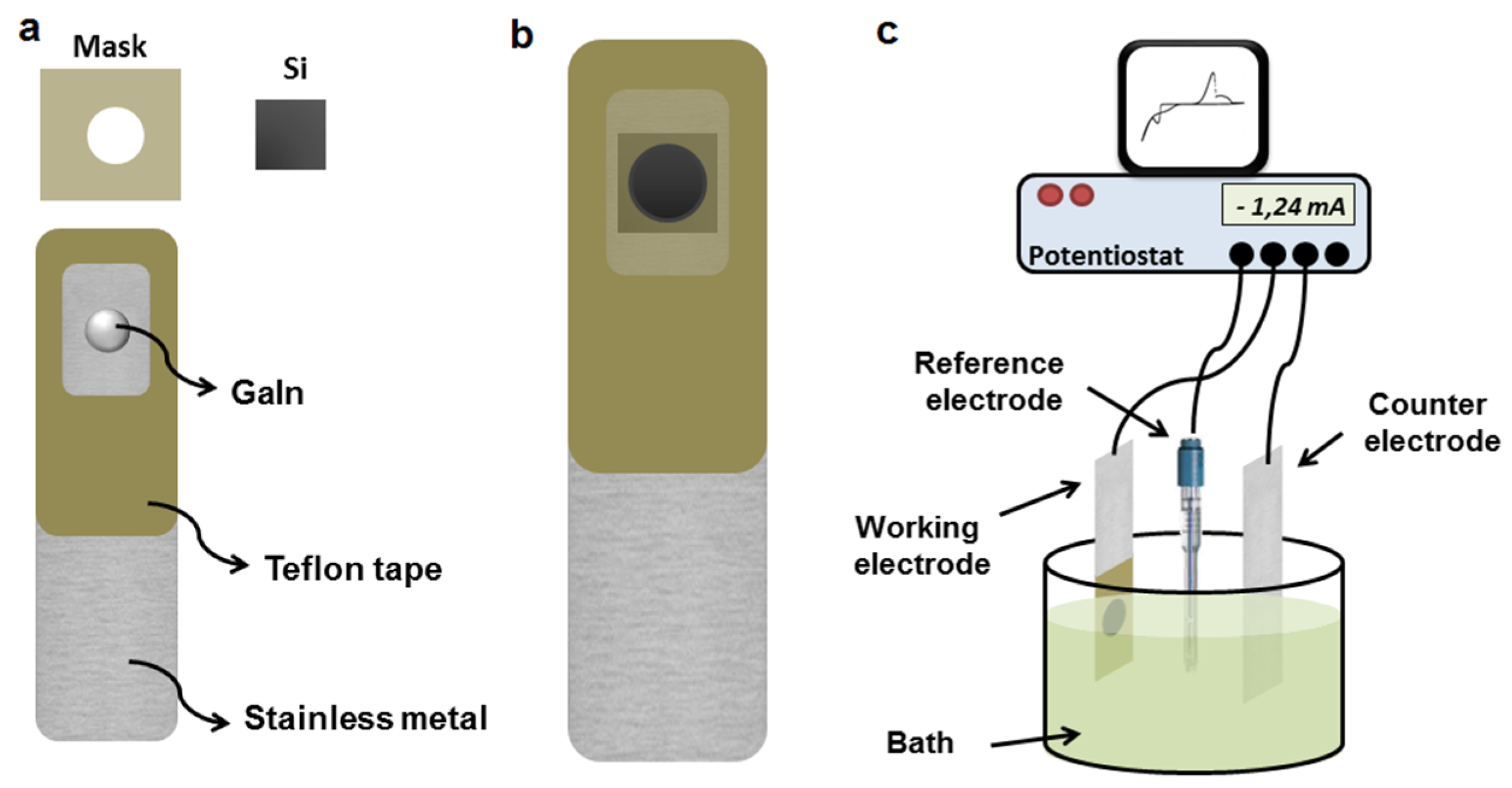
2. Materials and Methods

The electrodeposition was performed with a bath solution containing 30 mM FeSO4 + 700 mM NiSO4 + 20 mM NiCl2 + 16 mM Saccharin + 400 mM H3BO4, deposited directly onto (1,0,0) substrates of n-type silicon with resistivity of 1000 ohm × cm, which were previously cleaned in an ultrasonic bath of acetone and isopropyl alcohol for 15 min, rinsed with deionized water (18.2 MΩ·cm), and dipped in 10% HF for 15 s, to remove the native oxide layer. The used galvanostatic constant current was estimated by the cyclic voltammetry technique and a set of samples with different electrodeposition times were obtained with the potentiostat PGSTAT128N from Metrohm Autolab (Utrecht, The Nederlands). The current density used was −6.3 mA/cm² and the electrodeposition was performed over a circular area with 5 mm diameter, provided by application of an adhesive tape mask on the polished surface of the silicon substrates. GaIn alloy was applied to the rough surface of silicon substrates in order to provide an ohmic electrical contact between the silicon and the working electrode. The three electrodes utilized in the deposition cell (Figure 1) were a saturated calomel reference electrode, platinum counter electrode, and a stainless thin plate for supporting the silicon working electrode. The samples’ composition and crystallinity were obtained by X-ray diffractometry (XRD) (D8 Discover, Bruker, Billerica, MA, USA) whereas the film morphology was assessed by scanning electron microscopy (SEM) (eLINE Plus, Raith, Dortmund, Germany). Static magnetization investigation was carried out using home made magneto-optic Kerr effect magnetometry (MOKE) whereas dynamic magnetic properties were assessed using ferromagnetic resonance (FMR) (EMX PremiumX, Bruker, Billerica, MA, USA). In the FMR, the absorption of a constant microwave with a frequency of 9.5 GHz (X-band) was investigated while sweeping the applied DC magnetic field.
In order to better understand both the static and dynamic magnetization ( m ) behavior, micromagnetic simulation based on the Landau-Lifshitz equation was also performed:
δ m δ t = γ 1 + α 2 [ m × B e f f + α ( m × ( m × B e f f ) ) ]
with damping coefficient α, gyromagnetic ratio γ, and effective magnetic field B e f f , the latter including contributions from the external magnetic field B e x t and magnetostatic field B d e m a g depending on the saturation magnetization M s a t , magnetocrystalline anisotropy, and exchange interaction. The iterations for magnetization simulation of 3 × 3 × 3 nm3 meshes were performed with the accelerated GPU based software Mumax3 [25] whereas the theoretical FMR investigation was carried out with Mumax3 data analyses using the µ-FMR software [26].

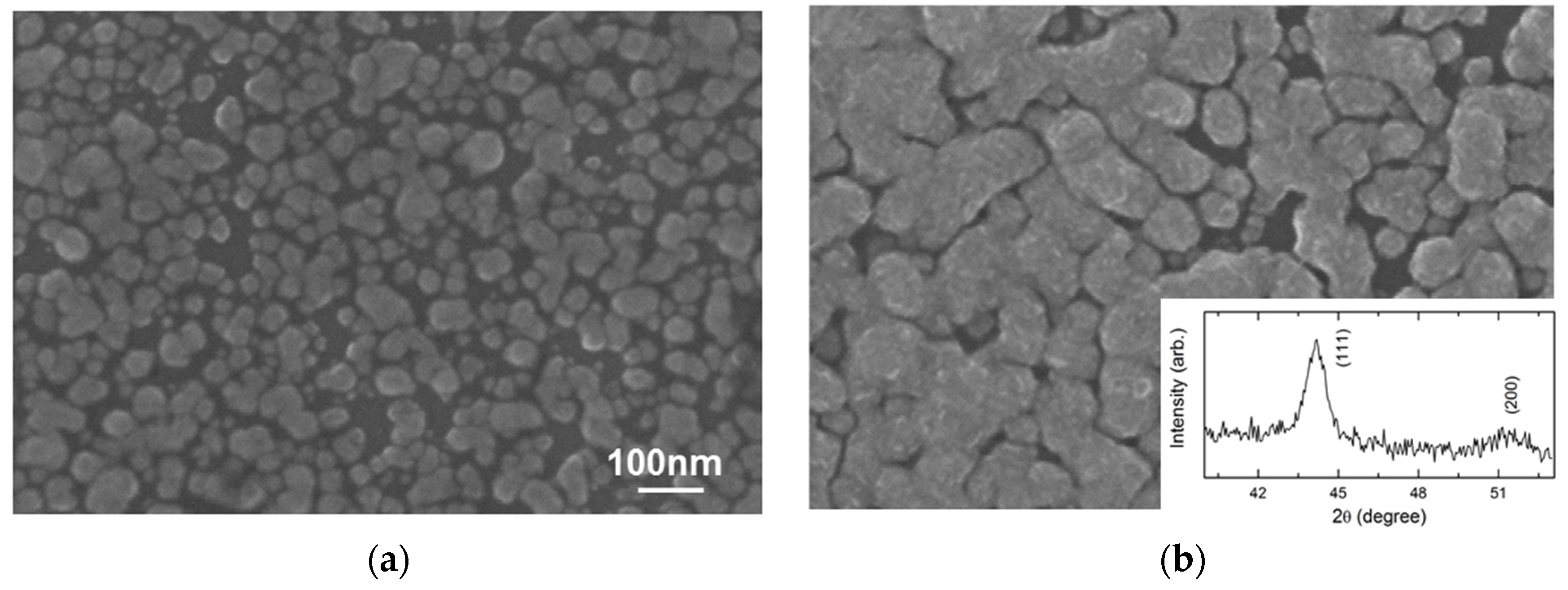
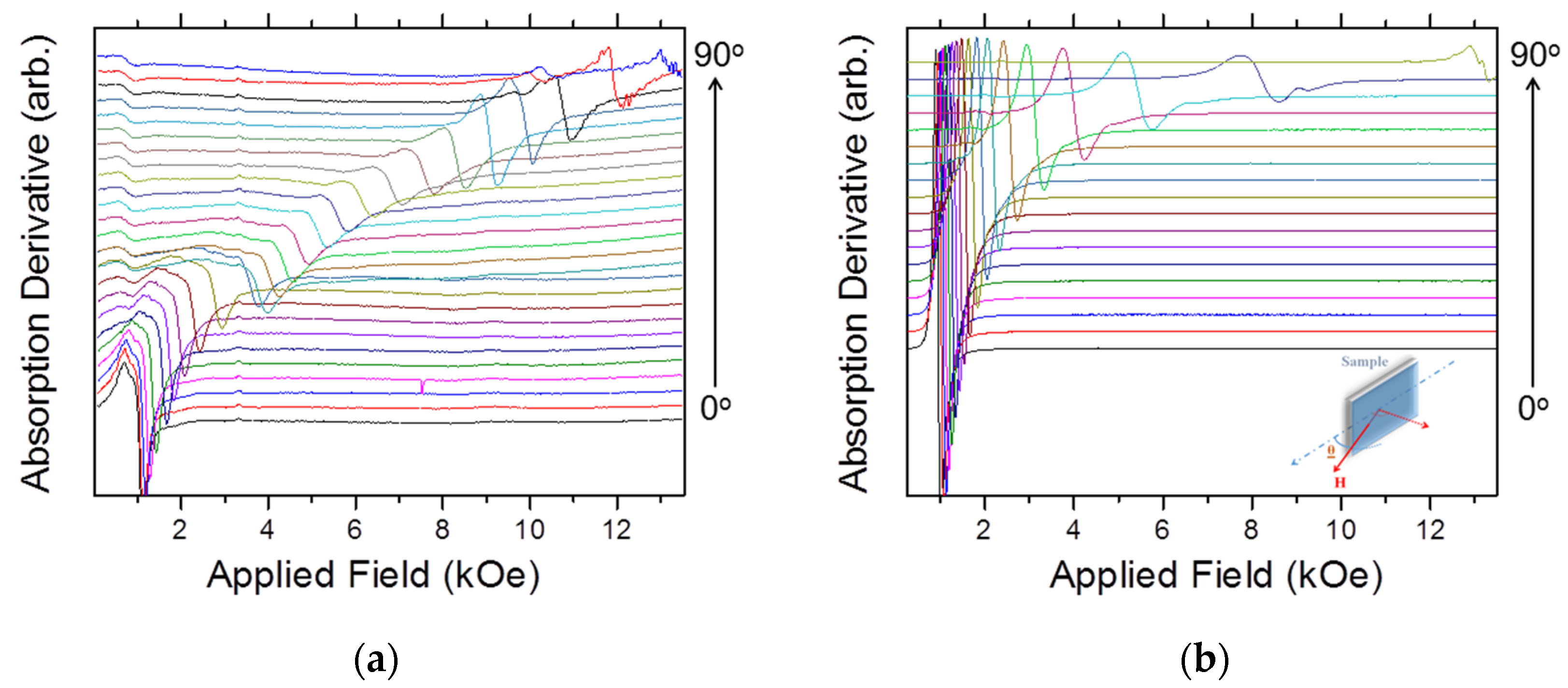
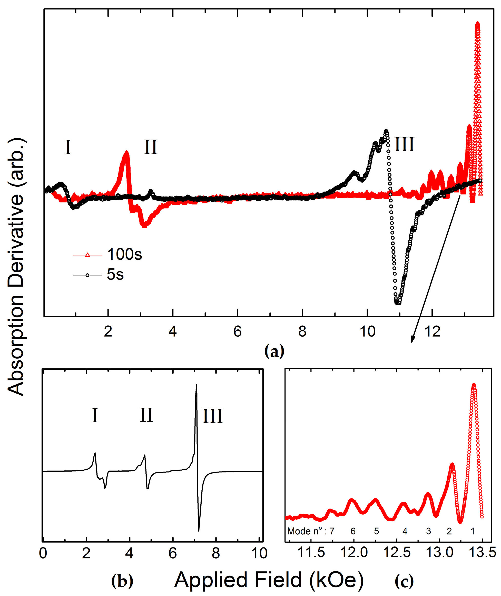
3. Results and Discussion

Figure 2a presents the cyclic voltammogram trace, obtained for the electrode and bath solution described above, which was analyzed and compared with previous works performed in non-degenerated silicon, in order to set the proper deposition current to obtain permalloy deposits onto highly resistive silicon substrates. Galvanostatic electrodeposition curves, obtained with different deposition times and under a constant current density of −6.3 mA/cm2, are presented in Figure 2b.
From the curves shown in Figure 2a, it was possible to verify the reproducibility of the as-deposited films. Electrical characterization was performed by two-point probe I–V measurements with contacts made by Ga-In alloy, which is a material known to present low resistive contact with silicon. From the plot of resistance vs. deposition time (see inset of Figure 2b) we were able to estimate the film percolation time of around 10 s. Indeed, the deposition evolves in time, first forming non-percolated nanoclusters, until percolation sets in with subsequent total covering of the substrate. These two regimes are clearly shown in the SEM micrographs presented in Figure 3a,b. The XRD data presented in the inset of Figure 3b shows the preferential (111) and (200) orientation of the permalloy thin film obtained by electrodeposition onto highly resistive n-type silicon substrates. Actually, this is the characteristic polycrystalline orientation for permalloy films reported in the literature [27].
The static magnetization behavior (MOKE measurements) of the samples, with electrodeposition times below and above the percolation threshold, is observed from the hysteresis curves presented in Figure 4a. The thin films with longer deposition times presented a low coercive field of 4 Oe and an abrupt magnetization direction change as a function of the sweeping external magnetic field, which are characteristic in percolated permalloy thin films. In the case of nanoclusters obtained with shorter deposition times, i.e., below the percolation limit, the magnetization direction changes slowly until saturation is reached. This behavior is regularly observed in the hysteresis of magnetic nanodisks [20] and it is attributed to the magnetic vortex configuration in the ground state, with magnetic moments in plane aligned clockwise or anticlockwise with the disk circular borders (chirality) and small up or down out-of-plane cores in the disk center (polarity) [28]. In Figure 4b we present the micromagnetic simulation performed with the permalloy film parameters; saturation magnetization 860 × 103 A/m, Exchange stiffness 13 × 10−12 J/m, Landau-Lifshitz damping constant 0.01, and geometries estimated from the SEM images. In the simulated hysteresis it is possible to note that the slow change in magnetization direction occurs due to the vortex core annihilation process, once the energy required for annihilation of the stable topologic vortex is much higher than that for domain wall movement in thin films.
The dynamical magnetization behavior as a function of the sample rotation angle, for samples below and above the percolation threshold, with applied DC magnetic field tilting around the normal sample direction are presented in Figure 5a,b, respectively.
We observed that the resonance fields of both samples are very close whereas the linewidth of the non-percolated sample is higher when the field is applied in the in-plane orientation (zero degree). The resonance field of the main peak in the percolated sample increases more abruptly than in the non-percolated one while films are tilted from in-plane to out-of-plane orientations with respect to the DC applied magnetic field. This effect is consistent with the magnetic behavior observed in the hysteresis curves and it is also related to the vortex magnetization. In the perpendicular orientation (out-of-plane configuration), as for the data presented in Figure 6a, two extra small peaks are observed in the measurements performed in the permalloy nanoclusters. Those peaks are also related to the vortex magnetization dynamics in the hemispherical structures. From the comparison between the experimental measurement and micromagnetic simulation presented in Figure 6b, it is possible to conclude that the lowest peak appears due to the resonance of vortex with polarization in the opposite sense to the applied DC field. With the increase of the external DC field, all vortex polarizations are aligned with the field and the second peak is related to the resonance mode of the field aligned vortex core. The last main peak in the simulation is attributed to the principal standing spin wave resonant mode. The perpendicular result for the percolated sample evidenced the very good quality of the permalloy thin film obtained by electrodeposition onto low doped n-type silicon substrate, with seven well-defined peaks related to the spin wave highlighted in Figure 6c [29].

4. Conclusions

We have performed an investigation of permalloy electrodeposition onto low doped n-type silicon substrates, from clusters under percolation to percolated thin films. The structural results show good quality of the percolated polycrystalline thin films. The static and dynamic magnetization behavior of the nanoclusters evidenced vortex magnetization with random chirality and polarization in order to minimize the dipolar interaction. The low dimensional stable topological vortex configuration obtained through electrodeposition has potential for applications in low-cost microwave magnetic sensors or magnetic memory devices.

Acknowledgments

This research was supported in Brazil by Conselho Nacional de Desenvolvimento Científico e Tecnológico (CNPq), Fundação de Apoio à Pesquisa do Distrito Federal (FAPDF), and Fundação de Amparo à Pesquisa do Estado de Minas Gerais (FAPEMIG). The authors also want to thank Luiz Sampaio from LABNANO-CBPF for the SEM images and MOKE measurements.

Author Contributions

C.I.L.d.A. planned and supervised the present study. K.F. and J.R.T. developed the samples and measured the static magnetization. The dynamic magnetization measurements were performed by J.F.F. and L.C.F. and micromagnetic simulations developed by C.I.L.d.A. and J.R.T. The manuscript was written by C.I.L.d.A. and P.C.M. and all the authors participated in the discussions.

Conflicts of Interest

The authors declare no conflict of interest.

References

  1. Jeffers, F. High-density magnetic recording head. Proc. IEEE 1986, 74, 1540–1556. [Google Scholar] [CrossRef]
  2. Hunt, R. A magnetoresistive readout transducer. IEEE Trans. Magn. 1971, 7, 150–154. [Google Scholar] [CrossRef]
  3. Mcguire, T.R.; Potter, R.I. Anisotropic magnetoresistance in ferromagnetic 3d alloys. IEEE Trans. Magn. 1975, 11, 1018–1038. [Google Scholar] [CrossRef]
  4. Girard, R. The electrodeposition of thin magnetic permalloy films. J. Appl. Phys. 1967, 38, 1423–1430. [Google Scholar] [CrossRef]
  5. Stobiecki, T.; Bełtowska-Lehman, E.; Riesenkampf, A. The preparation and properties of electrodeposited permalloy films on substrates of evaporated permalloy. Thin Solid Films 1975, 29, 313–318. [Google Scholar] [CrossRef]
  6. Butta, M. Effect of saccharin in electroplated NiFe alloy on the noise of fluxgate. IEEE Trans. Magn. 2016, 52, 1–4. [Google Scholar] [CrossRef]
  7. Lamrani, S.; Guittoum, A.; Schäfer, R.; Hemmous, M.; Neu, V.; Pofahl, S.; Hadjersi, T.; Benbrahim, N. Morphology, structure and magnetic study of permalloy films electroplated on silicon nanowires. J. Magn. Magn. Mater. 2015, 396, 263–267. [Google Scholar] [CrossRef]
  8. IKamo, Y.; Miyamoto, T. Preparation and Magnetic Properties of Electrodeposited Permalloy Film. IEEE Trans. J. Magn. Jpn. 1985, 1, 502–504. [Google Scholar]
  9. Steven, D.L.; Shirley, R.; Daniel, T.S. Characterization of NixFe1−x (0.10 < x < 0.95) Electrodeposition from a Family of Sulfamate-Chloride Electrolytes. J. Electrochem. Soc. 1999, 146, 1431–1435. [Google Scholar]
  10. Monsma, D.J.; Lodder, J.C.; Popma, Th.J.A.; Dieny, B. Perpendicular Hot Electron Spin-Valve Effect in a New Magnetic Field Sensor: The Spin-Valve Transistor. Phys. Rev. Lett. 1995, 74, 5260. [Google Scholar] [CrossRef] [PubMed]
  11. Datta, S.; Das, B. Electronic analog of the electro-optic modulator. Appl. Phys. Lett. 1990, 56, 665. [Google Scholar] [CrossRef]
  12. Dlubak, B.; Martin, M.-B.; Deranlot, C.; Servet, B.; Xavier, S.; Mattana, R.; Sprinkle, M.; Berger, C.; De Heer, W.A.; Petroff, F.; et al. Highly efficient spin transport in epitaxial graphene on SiC. Nat. Phys. 2012, 8, 557–561. [Google Scholar] [CrossRef]
  13. Spada, E.R.; de Oliveira, L.S.; da Rocha, A.S.; Pasa, A.A.; Zangari, G.; Sartorelli, M.L. Thin films of FexNi1−x electroplated on silicon (100). J. Magn. Magn. Mater. 2004, 272, E891–E892. [Google Scholar] [CrossRef]
  14. De Araujo, C.I. L.; Munford, M.L.; Delatorre, R.G.; Da Cas, A.V.; Zoldan, V.C.; Pasa, A.A.; Garcia, N.G. Spin polarized current in permalloy clusters electrodeposited on silicon: Two-dimensional giant magnetoresistance. Appl. Phys. Lett. 2008, 92, 222101. [Google Scholar] [CrossRef]
  15. De Araujo, C.I.L.; Fonseca, J.M.; Sinnecker, J.P.; Delatorre, R.G.; Garcia, N.; Pasa, A.A. Circular single domains in hemispherical permalloy nanoclusters. J. Appl. Phys. 2014, 116, 183906. [Google Scholar] [CrossRef]
  16. Rahm, M.; Stah, J.; Weiss, D. Programmable logic elements based on ferromagnetic nanodisks containing two antidots. Appl. Phys. Lett. 2005, 87, 182107. [Google Scholar] [CrossRef]
  17. Iwasaki, J.; Mochizuki, M.; Nagaosa, N. Current-induced skyrmion dynamics in constricted geometries. Nat. Nanotechnol. 2013, 8, 742–747. [Google Scholar] [CrossRef] [PubMed]
  18. Kim, D.-H.; Rozhkova, E.A.; Ulasov, I.V.; Bader, S.D.; Rajh, T.; Lesniak, M.S.; Novosad, V. Biofunctionalized magnetic-vortex microdiscs for targeted cancer-cell destruction. Nat. Mater. 2010, 9, 165–171. [Google Scholar] [CrossRef] [PubMed]
  19. Metlov, K.L.; Lee, Y. Map of metastable states for thin circular magnetic nanocylinders. Appl. Phys. Lett. 2008, 92, 112506. [Google Scholar] [CrossRef]
  20. Cowburn, R.P.; Koltsov, D.K.; Adeyeye, A.O.; Welland, M.E.; Tricker, D.M. Single-Domain Circular Nanomagnets. Phys. Rev. Lett. 1999, 83, 1042. [Google Scholar] [CrossRef]
  21. Dzyaloshinsky, I. A thermodynamic theory of “weak” ferromagnetism of antiferromagnetics. J. Phys. Chem. Solids 1958, 4, 241–255. [Google Scholar] [CrossRef]
  22. Moriya, T. Anisotropic Superexchange Interaction and Weak Ferromagnetism. Phys. Rev. 1960, 120, 91. [Google Scholar] [CrossRef]
  23. De Araujo, C.I.L.; Alves, S.G.; Buda-Prejbeanu, L.D.; Dieny, B. Multilevel Thermally Assisted Magnetoresistive Random-Access Memory Based on Exchange-Biased Vortex Configurations. Phys. Rev. Appl. 2016, 6, 024015. [Google Scholar] [CrossRef]
  24. Chang, L.-T.; Fischer, I.A.; Tang, J.; Wang, C.-Y.; Yu, G.; Fan, Y.; Murata, K.; Nie, T.; Oehme, M.; Schulze, J.; et al. Electrical detection of spin transport in Si two-dimensional electron gas systems. Nanotechnology 2016, 27, 36. [Google Scholar] [CrossRef] [PubMed]
  25. Vansteenkiste, A.; Leliaert, J.; Dvornik, M.; Helsen, M.; Garcia-Sanchez, F.; Waeyenberge, B.V. The design and verification of MuMax3. AIP Adv. 2014, 4, 107133. [Google Scholar] [CrossRef] [Green Version]
  26. De Araujo, C.I.L.; Rizzi, L.G. µ-FMR—An analysis program to extract the ferromagnetic resonance absorption spectrum from micromagnetic simulations. To be submitted for publication. 2017. [Google Scholar]
  27. Kanak, J.; Stobiecki, T.; Wisniowski, P.; Gladyszewski, G.; Maass, W.; Szymanski, B. XRD study of the structure of NiFe/Au and NiFe/Cu Superlattices. J. Magn. Magn. Mater. 2002, 239, 329–331. [Google Scholar] [CrossRef]
  28. Samardak, A.; Sukovatitsina, E.; Ognev, A.; Stebliy, M.; Davydenko, A.; Chebotkevich, L.; Kim, Y.K.; Forough Nasirpouri, F.; Janjan, S.-M.; Nasirpouri, F. Magnetic vortex state and multi-domain pattern in electrodeposited hemispherical nanogranular nickel films. J. Magn. Magn. Mater. 2014, 371, 149–156. [Google Scholar] [CrossRef]
  29. Seavey, M.H., Jr.; Tannenwald, P.E. Direct observation of spin-wave resonance. Phys. Rev. Lett. 1958, 5, 168. [Google Scholar] [CrossRef]
Figure 1. (a) Components involved for mounting the working electrode. Teflon tape is used to prevent the contact between the stainless metal and the electrolyte. (b) Complete working electrode assembly and (c) Representation of the electrochemical cell.
Coatings 07 00033 g001
Figure 2. (a) Cyclic voltammogram trace for Permalloy on highly resistive n-type silicon and (b) Galvanostatic deposition transient for different deposition times. The extrapolation of resistances obtained from the I–V curves as a function of the deposition time (see inset of (b)), provides the estimated percolation time of 10 s.
Coatings 07 00033 g002
Figure 3. (a) Scanning electron micrograph of the sample under percolation obtained by an electrodeposition time of 5 s; (b) Scanning electron micrograph of the sample over percolation, obtained by an electrodeposition time of 15 s. The inset in (b) shows the results of XRD performed on the sample with a 100 s electrodeposition time, showing the preferential (111) and (200) orientation characteristic of permalloy material. The scale bar is the same for both images.
Coatings 07 00033 g003
Figure 4. (a) Hysteresis curves obtained from MOKE measurements in samples with an electrodeposition time of 5 s and 15 s, under and over the percolation threshold, respectively, and (b) Theoretical hysteresis curve realized by micromagnetic simulation in an array of hemispheres with 90 nm diameters. The inset in (b) shows the saturated magnetization (upper left) and magnetic vortex ground state (lower right).
Coatings 07 00033 g004
Figure 5. Ferromagnetic resonance measurements obtained as a function of out-of-plane angle tilting (inset) from an external DC field applied parallel to the sample plane (0°) and normal orientation (90°) for samples grown by an electrodeposition time of (a) 5 s and (b) 100 s.
Coatings 07 00033 g005
Figure 6. (a) Perpendicular ferromagnetic resonance measured in samples electrodeposited for 5 s and 100 s; (b) dynamic micromagnetic simulation results for the unpercolated model as presented in Figure 3 and (c) a zoomed view of standing spin wave modes that are well defined in the percolated sample.
Coatings 07 00033 g006

