Article

Antireflection Coatings for Strongly Curved Glass Lenses by Atomic Layer Deposition

by
Kristin Pfeiffer
1,*,
Ulrike Schulz
2,
Andreas Tünnermann
1,2 and
Adriana Szeghalmi
1,2,*
1
Institute of Applied Physics, Abbe Center of Photonics, Friedrich Schiller University Jena, Albert-Einstein-Str. 15, 07745 Jena, Germany
2
Fraunhofer Institute for Applied Optics and Precision Engineering, Albert-Einstein-Str. 7, 07745 Jena, Germany
*
Authors to whom correspondence should be addressed.
Coatings 2017, 7(8), 118; https://doi.org/10.3390/coatings7080118
Submission received: 12 June 2017 / Revised: 3 August 2017 / Accepted: 3 August 2017 / Published: 9 August 2017
(This article belongs to the Special Issue Antireflective Coatings for Glass and Transparent Polymers)

Abstract

:
Antireflection (AR) coatings are indispensable in numerous optical applications and are increasingly demanded on highly curved optical components. In this work, optical thin films of SiO2, Al2O3, TiO2 and Ta2O5 were prepared by atomic layer deposition (ALD), which is based on self-limiting surface reactions leading to a uniform film thickness on arbitrarily shaped surfaces. Al2O3/TiO2/SiO2 and Al2O3/Ta2O5/SiO2 AR coatings were successfully applied in the 400–750 nm and 400–700 nm spectral range, respectively. Less than 0.6% reflectance with an average of 0.3% has been measured on a fused silica hemispherical (half-ball) lens with 4 mm diameter along the entire lens surface at 0° angle of incidence. The reflectance on a large B270 aspherical lens with height of 25 mm and diameter of 50 mm decreased to less than 1% with an average reflectance < 0.3%. The results demonstrate that ALD is a promising technology for deposition of uniform optical layers on strongly curved lenses without complex in situ thickness monitoring.

1. Introduction

Most optical systems contain a large number of lenses or other optical elements. Reflections at each interface reduce the intensity of the transmitted light and thus the overall efficiency of the systems. Reflection losses can be greatly reduced by applying antireflection (AR) coatings to the optical surfaces [1,2,3,4]. In addition, AR coatings attenuate the effect of ghost images that are caused by multiple reflection of light from lens surfaces. Optical interference coatings that are typically thin film multilayers of high-refractive and low-refractive index materials demand precise thickness control of each layer. Commonly, thin films applied in precision optics are produced by physical vapor deposition (PVD) [5,6]. Due to the line-of-sight nature of PVD, the surface of a convex lens that is normal to the deposition flux receives a higher amount of material than the edges of the lens. As indicated in Figure 1a, significant thickness gradients might occur on highly curved lenses. Consequently, the required film thickness might not be met over the entire surface of the lens, leading to a distortion of the resulting transmittance spectra. To achieve a better uniformity on curved substrates, complex technical modifications are necessary when using PVD methods, that includes f.e. the constant rotating and tilting of the lens during the deposition, with or without the usage of complicated shadowing masks [7,8,9,10]. Antireflection nanostructures are another approach to reduce reflection losses at curved surfaces [11,12,13]. Nevertheless, for outer lenses of optical systems multilayer AR coatings are preferably used due to their better cleanability and mechanical stability.
Atomic layer deposition (ALD) is an alternative and promising technology for uniform multilayer optical coatings [14,15,16,17,18]. We have previously shown a broadband AR coating on flat high refractive index glasses using SiO2/HfO2 multilayers [19]. Atomic layer deposition is also being considered for more complex interference coatings such as dichroic mirrors and narrow bandpass filters [16,20,21]. Atomic layer deposition is a modified form of chemical vapor deposition, where the precursors are sequentially exposed to the surface until saturation is reached [22]. Precursor pulses are separated by inert gas purging; as a result, no gas-phase reactions can take place and the chemical reactions are limited to the surface, see Figure 1b. A typical ALD cycle for the deposition of metal oxides contains four steps: precursor pulse, inert gas purge, oxidizing pulse and inert gas purge. In the case of precursors with low chemical reactivity, often a hold step is introduced after the precursor pulse. Hence, the precursor is trapped in the reactor to entirely react with the surface active groups. Due to this cyclic surface-controlled growth, ALD inherently offers precise thickness control, good thickness uniformity and high reproducibility. It is well known for its conformal film growth on complex nanostructures with high aspect ratios [23,24]. In this work, the capability of ALD for deposition of antireflection coatings on highly curved lenses has been analyzed.
This paper first discusses single-layer properties and thickness uniformity of the SiO2, Al2O3, TiO2, and Ta2O5 coatings, then an AR design and its adjustment to the ALD coating is presented on flat glass substrates. Finally, ALD antireflection coatings are demonstrated on curved lenses, firstly on a half-ball lens and secondly on an asphere.

2. Materials and Methods

ALD-deposited SiO2, Al2O3, Ta2O5 and TiO2 thin films were used for the antireflection coatings. Depositions were carried out in an Oxford Instruments (Bristol, United Kingdom) OpAL™ ALD reactor and a Picosun Oy (Espoo, Finland) Sunale™ R200 ALD reactor with a showerhead setup for single-wafer processing. In the OpAL tool, thin films have been grown by plasma-enhanced ALD (PEALD) at substrate temperatures of 100 °C. In the Sunale tool, thermal ALD processes were performed at 300 °C.
All metal oxide films were grown from commercially available precursors. The low-index material SiO2 was deposited using tris[dimethylamino]silane (3DMAS). Trimethylaluminium (TMA) was applied to deposit the mid-refractive index material Al2O3. The high-index materials TiO2 and Ta2O5 were deposited from titanium(IV)isopropoxide (TTIP) and tantalum(V)ethoxide (Ta(OEt)5), respectively. Process parameters are summarized in Table 1.
The growth rates and the optical properties of the ALD thin films are determined from single-layer experiments on flat substrates. The growth rates (growth per cycles, GPC) were determined on Si samples by measuring the film thickness with a J.A. Woollam Co. (Lincoln, NV, USA) M-2000® spectroscopic ellipsometer. A Sentech Instruments GmbH (Berlin, Germany) SE850 spectroscopic ellipsometer was used for uniformity mapping of the film thickness on an 8 inch (200 mm) silicon wafer over 180 mm central area on the wafer.
Refractive indices were determined by spectrophotometry of 200 to 300 nm thin films coated on fused silica samples. The reflectance and transmittance spectra were measured with a PerkinElmer, Inc. (Waltham, MA, USA) Lambda 950 spectrophotometer equipped with a home-build accessory for absolute reflectance measurements [25].
For demonstration purposes, antireflection (AR) coatings were applied to a half-ball lens with a diameter of 4 mm and to an aspheric lens with a diameter of 50 mm and a center thickness of 25 mm. An Olympus K. K. USPM-RU-W NIR micro-spectrophotometer (Tokio, Japan) was used to measure the reflectance from a minute spot on different positions of the lens, whereas the lens is placed on a tilt stage and tilted to angles up to 60°. The tilted lens is then moved in the x-, y- and z-direction so that the light from a fixed source is focused on the lens surface and the light rays are perpendicular to the surface (AOI = 0°).

3. Results and Discussion

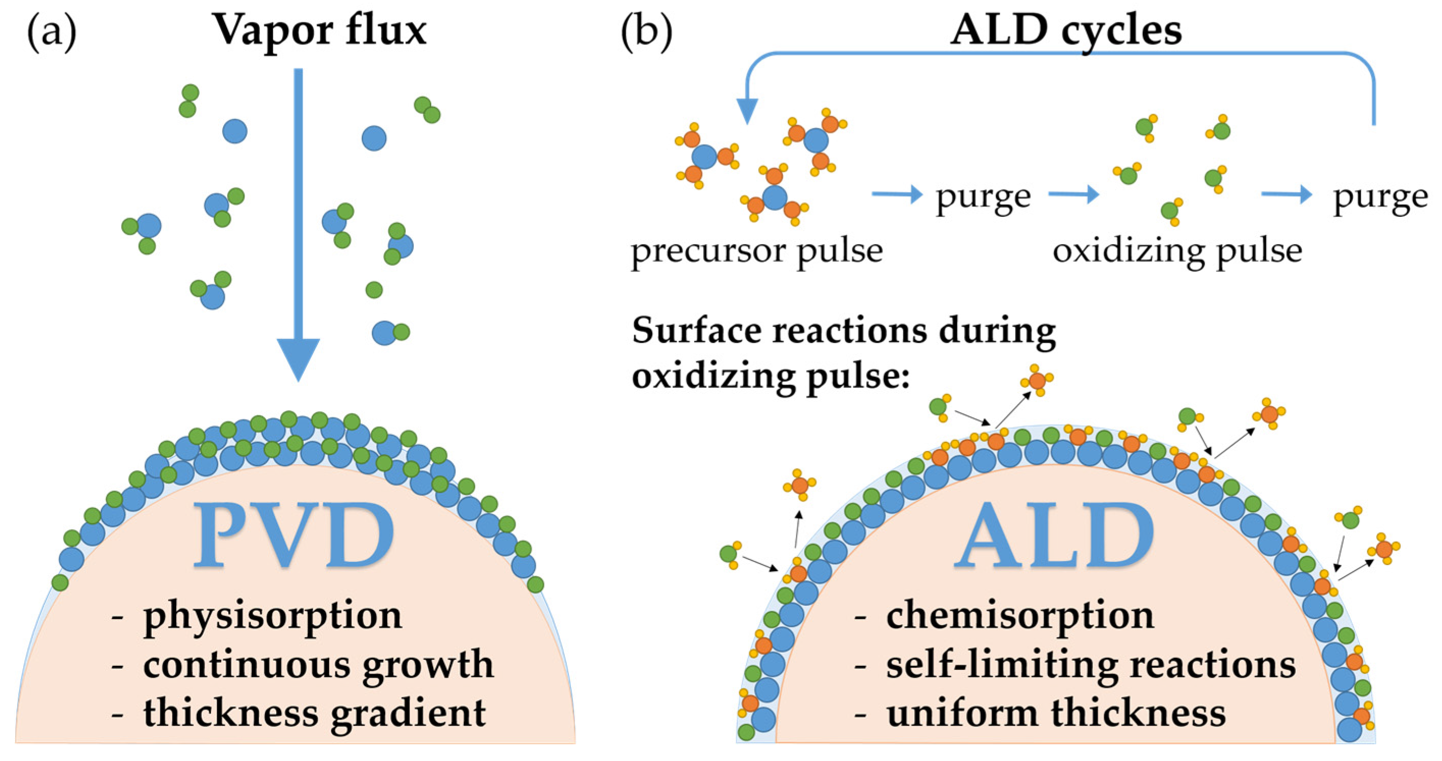
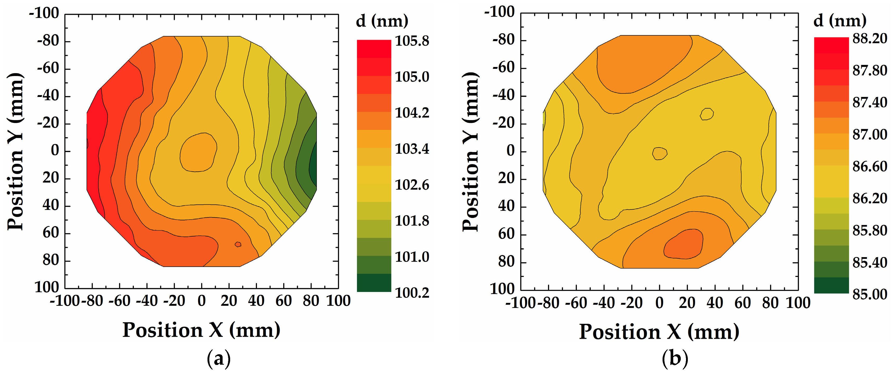
3.1. Characterization of ALD Thin Films

ALD processes for dielectric thin films have frequently been reported, whereas Al2O3 is the most investigated ALD material [26,27]. Al2O3 has been applied in ALD antireflection coatings in combination with TiO2 [17,20] or Ta2O5 [28]. Next to this, SiO2 is a very important low-index material that we recently applied in ALD optical coatings [19,21,28,29]. The properties of the single-layer films resulting from the ALD processes used in this work are summarized in Table 2. The listed GPC values have been used to calculate the necessary ALD cycles to reach the thicknesses of each layer of the following AR coatings.
Growth rates and refractive index of SiO2 thin films are similar to films grown from other commercially available precursors, as BDEAS, BTBAS and AP-LTO®330 [30,31]. Alumina ALD thin films show a lower refractive index at lower deposition temperature [32] owing to a lower density at lower deposition temperatures [26]. The lower GPC of Al2O3 at higher deposition temperatures is attributed to less OH groups on the surface. Determined growth rates of Ta2O5 are comparable to growth rates reported for Ta2O5 thin films deposited using H2O and Ta(OEt)5, Ta(NEt2)3 or Ta(NEt)(NEt2)3 [33,34,35]. The reported GPC for PEALD TiO2 using TTIP in the range of 0.3–0.6 Å/cycle are relatively low, whereas thin films grown from TDMAT, Ti-Prime or Ti-Star have slightly higher growth rates than films grown from TTIP [36,37,38].
Very good lateral film thickness uniformity in the reactor is a prerequisite to ensure a uniform coating on a lens surface. However, non-uniformity in ALD processes is not explicitly analyzed in most research articles. Most tool providers guarantee a standard deviation of the ALD coatings of ca. 1%–3% depending on the material and process conditions. Noteworthy, the upscaling of ALD processes in batch reactors with similar non-uniformity distribution on larger-area batches is feasible [16]. The ALD coatings deposited in the OpAL research tool have thickness non-uniformities (NU%), defined as (dmax dmin)/2daverage × 100, of about ±1.5% (Al2O3, SiO2) and ±2.0% (TiO2). The processes in the Sunale R200 ALD reactor result in a thickness non-uniformity of about ±2.1% for Al2O3 and ±4.0% for Ta2O5, see Table 2. Elers et al. [39] discussed the sources of non-uniformities in ALD processes including overlapping precursor pulses due to short purge times, death pockets, etc., but also non-uniform gas and temperature distributions in the reactor chamber.
Figure 2a shows the surface mapping of a 200 mm wafer after thermal Al2O3 ALD process using 1156 cycles (TMA + H2O). The alumina film thickness on the wafer in this thermal process does not show a statistical random distribution, but a specific and well-reproducible lower film thickness on the right side of the reactor chamber than on the left side. Interestingly, the precursor and purge gas inlet is on the side where lower film thickness is measured indicating that the precursor dose is sufficient. There might be a temperature gradient on the wafer due to the gases entering the reactor on the right side or the purge time and gas flow might be not sufficient due to inadequate inert gas distribution. In PEALD processes, rather concentric thickness contour lines have been observed (not shown here), whereby the maximum position can be adjusted by the flow rates of the precursor and purge gas. We have demonstrated the possibility to improve the film thickness uniformities by rotating the substrate. Figure 2b depicts a thickness mapping of a wafer where the thermal Al2O3 ALD process was stopped after 500 cycles, the wafer manually rotated by 180° and the process continued for another 500 cycles. The wafer rotation could significantly improve the thickness non-uniformity from 2.4% to 0.6%, calculated from 392 mapping points on a 180 mm wafer area.

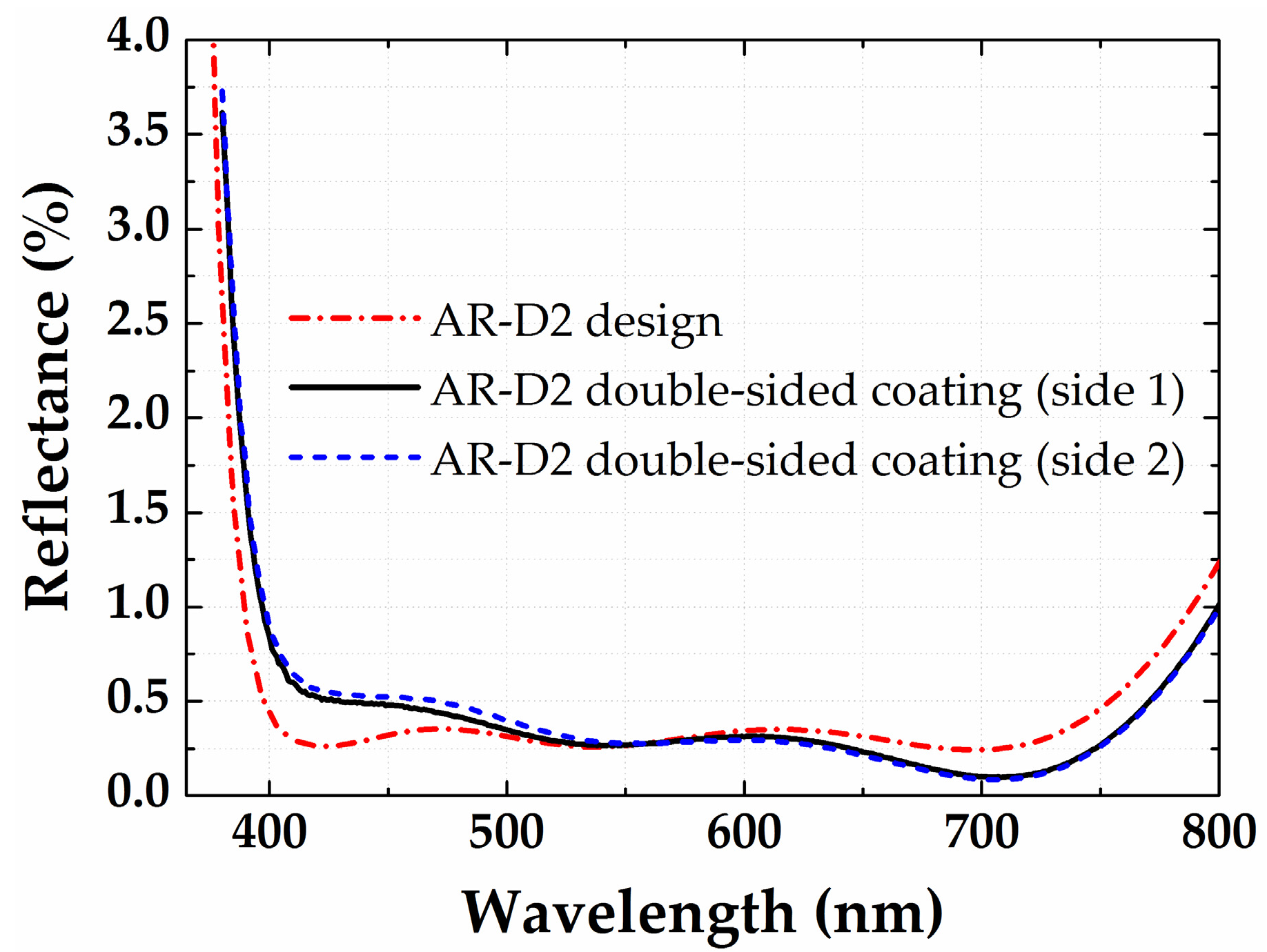
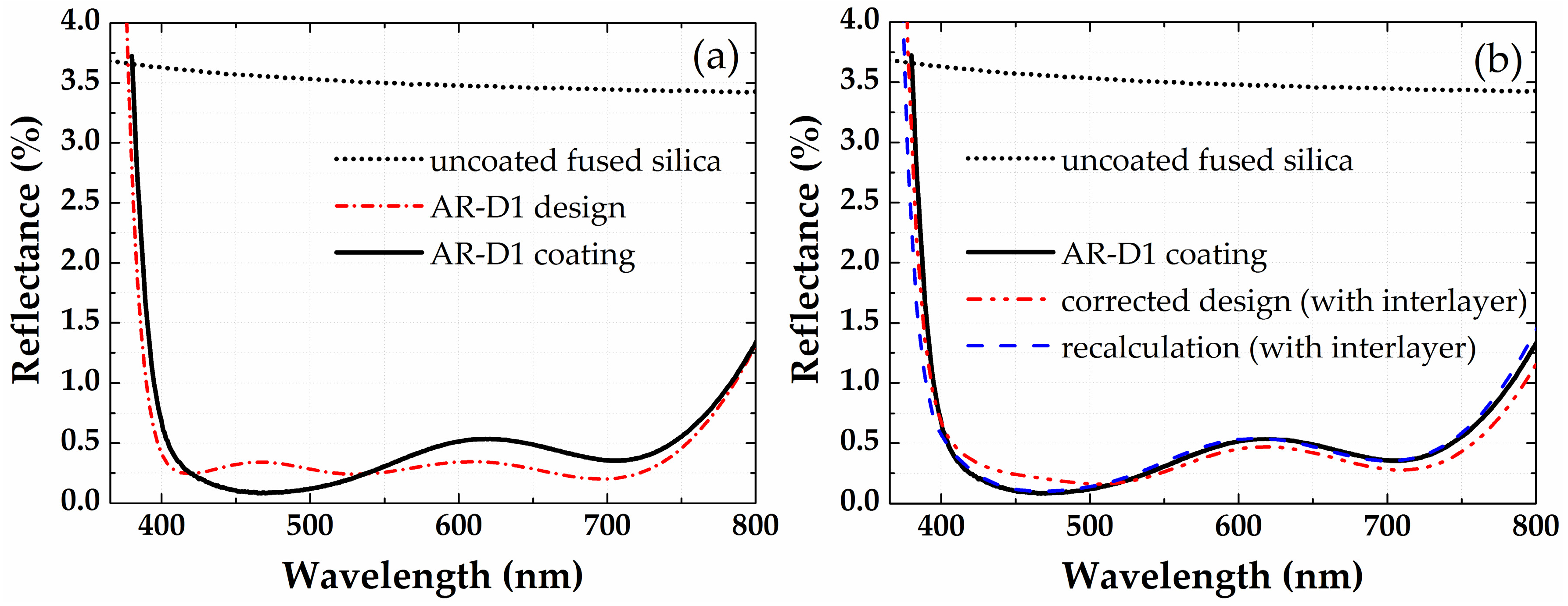
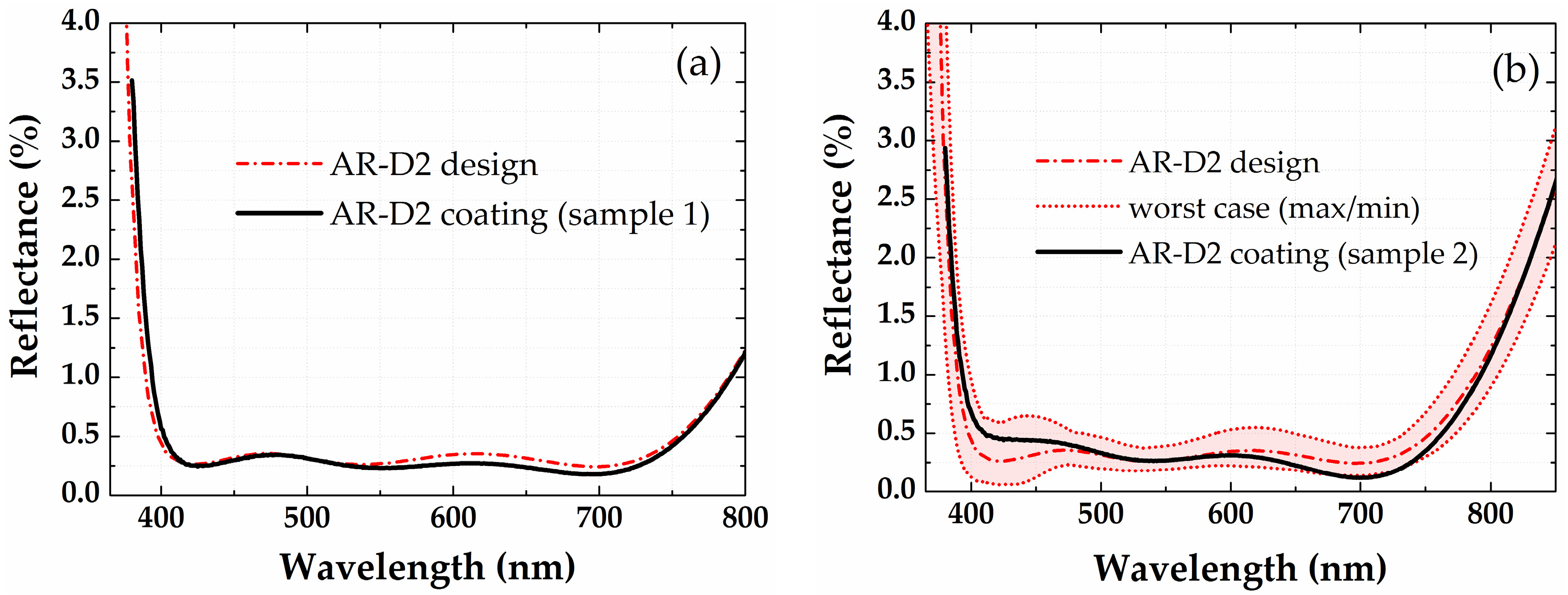
3.2. Antireflection Coatings on Plane Glass Substrates

An AR design consisting of seven layers has been calculated using the thin film software OptiLayer (version 11.65e, OptiLayer GmbH, Garching, Germany) to reduce the residual reflectance of a fused silica substrate from approximately 3.5% to less than 0.5% in the visible spectral range from 400 to 750 nm. Silicon dioxide was chosen as final layer, as its low refractive index will significantly improve the performance of the AR coating. ALD oxide films are typically amorphous, especially when deposited at low temperatures [40]. However, TiO2 ALD thin films tend to crystallize at moderate deposition temperatures. The growth of crystallites leads to high surface roughness and, as a result, strong scattering of light. The surface roughness significantly increases for film thicknesses greater than about 40 nm [41]. The crystallization can be inhibited by inserting a thin Al2O3 interlayer [42]. In the first design AR-D1 (Table 3) this interlayer was not included into the design, whereas experimentally, the thick 63.9 nm TiO2 has been split in two thinner TiO2 layers by introducing a 1.5 nm thin Al2O3 interlayer to inhibit the crystallization.
The AR coating was first tested on a plane substrate. By applying the AR-D1 coating to a fused silica glass sample, the reflectance could be reduced to an average reflectance of 0.3% in the visible spectral range from 400 to 750 nm, see Figure 3a. Comparing the reflectance spectra, the AR-D1 coating shows a deviation from the AR-D1 design. It was found that the misfit between design and coating has two origins. First, the 1.5 nm thin Al2O3 layer needs to be taken into account when designing the AR coating. This presumption is based on the good agreement of the measured spectrum to calculated expected one that includes the interlayer, see Figure 3b. Thin ALD layers are well known to be very dense and pinhole-free and are intensively investigated for barrier coating [43]. Therefore, the reflections at the interfaces of this ultra-thin layer must be considered in the optical design.
Second, a recalculation of the actual thicknesses from the measured spectra using the Film Wizard™ software (version 8.5.0, Scientific Computing International, Carlsbad, CA, USA) showed that Al2O3 layers on TiO2 are thinner as expected. The GPC on the underlying TiO2 is only 1.17 Å/cycle instead of 1.21 Å/cycle on Si or fused silica. Also, SiO2 thin films have a lower GPC on the underlying TiO2 films of only 1.17 Å/cycle instead of the expected 1.20 Å/cycle. Altered growth rates on different substrates have been repeatedly observed and are possibly a reason of different OH group concentrations or irregular OH group distributions on the underlying surface [17].
The film thickness deviation has been 0.4 and 0.6 nm for the alumina layers and approximately 2 nm for silica. This deviation in film thicknesses results in slight deviation of the measured curve (coating AR-D1) and the corrected design curve in Figure 3b. Note that no in situ control of the film thicknesses has been applied during the ALD process. In situ monitoring might be necessary for more complex AR coatings or interference coatings such as narrow bandpass filters or dichroic mirrors [20,21].
A second AR coating AR-D2 was designed including the Al2O3 interlayer. Furthermore, the adapted GPC values were used for calculating the necessary ALD cycles of Al2O3 and SiO2 layers on TiO2, see Table 2. By applying these two corrections, the reflectance of the design and the coating are in an excellent agreement for a sample that was placed in the center of the substrate table, see Figure 4a.
As the thickness non-uniformity was expected to be the main origin of errors, a worst-case analysis was performed, whereas the maximum allowed thickness deviation was specified as the expected NU% of each material, see Table 2. The area between the dotted lines in Figure 4b indicates the worst-case error corridor of the calculated maximum possible deviations from the theoretical reflectance spectra. To estimate the influence of the NU experimentally, next to the fused silica substrate (sample 1) that was placed in the middle of the substrate table, a second substrate (sample 2) was positioned at approximately 75 mm from the center of the table during the deposition. The measured reflectance spectra of sample 2 lies within the worst-case error corridor, indicating that the small deviations to the AR design are most likely a consequence of the lateral film thickness non-uniformity on the substrate table.

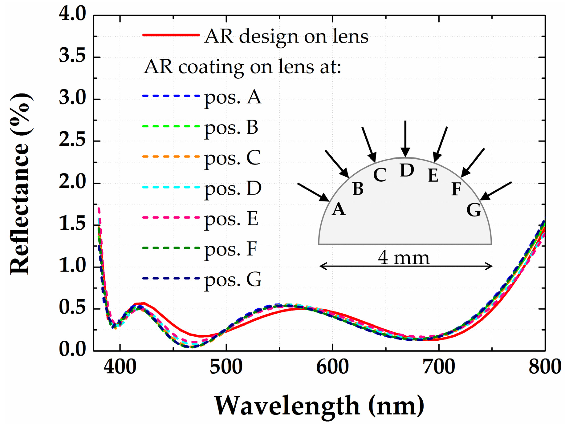
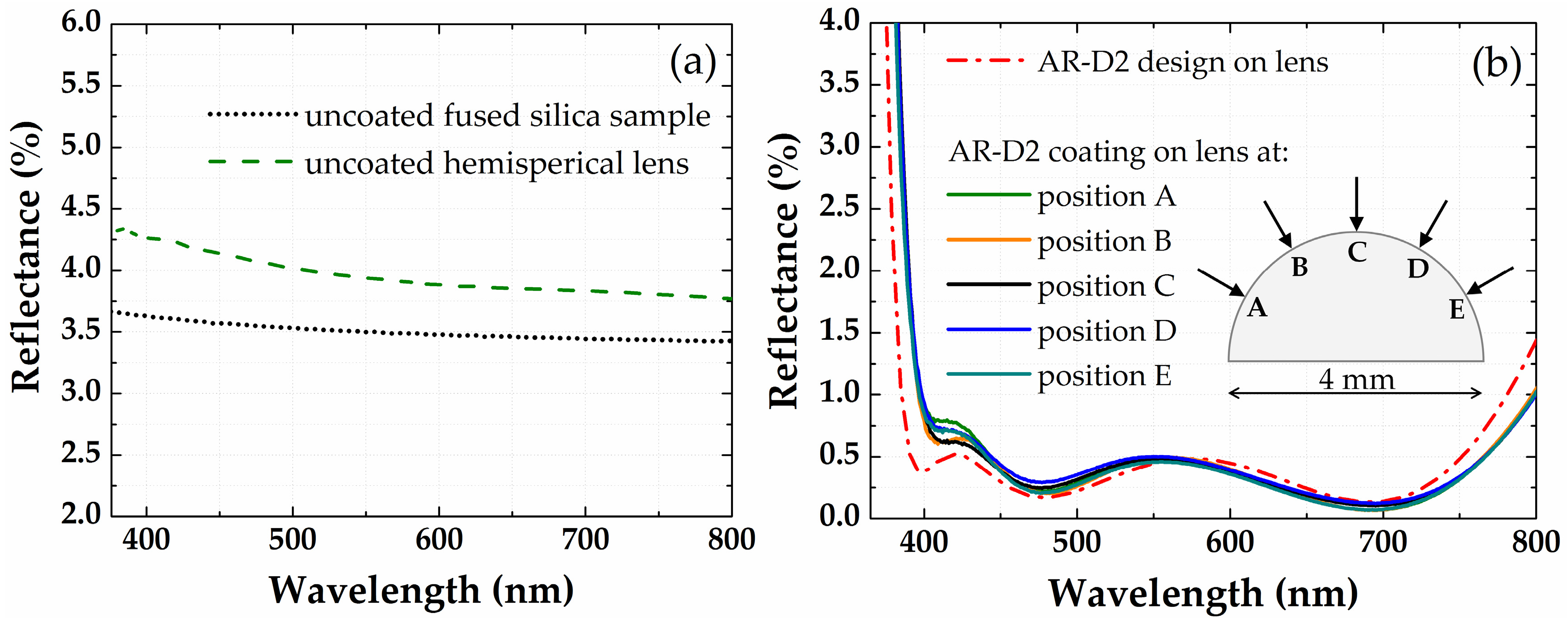
3.3. Antireflection Coatings on a Half-Ball Lens

The antireflection coating AR-D2 was applied to a hemispherical lens. The refractive index of the lens was calculated from the measured reflectance spectra of the uncoated half-ball lens, which is slightly higher than the reflectance of the fused silica glass substrate, see Figure 5a. Due to the higher effective refractive index of the bare lens, the appearance of the expected and measured AR spectra on the lens differs from the spectra on the coated glass slab (compare Figure 4a and Figure 5b). The measured spectra of the AR coating on the lens is in good agreement with the adapted AR design (Figure 5b).
It should be emphasized that the reflectance spectra are consistent at all positions on the lens. Hence, the AR coating was deposited uniformly on the hemispherical lens without any complex equipment to control the layer thickness.
An upright-positioned glass sample was used as reference sample for the edge of the glass plate since it is not possible to measure the reflectance at the very edge of the lens. As shown in Figure 6, the measured reflectance is in very good agreement with the design. The deposition occurs simultaneously on both sides of the glass sample and the measured spectra are identical on both sides of the substrates. The results show that the ALD-technology is not restricted to the radius of curvature.
The AR performance of the coated lens depends on the position in the chamber due to the lateral thickness non-uniformity. Hence, it has been possible to obtain an excellent AR coating on a curved lens matching very well the design curve, see Figure 7.

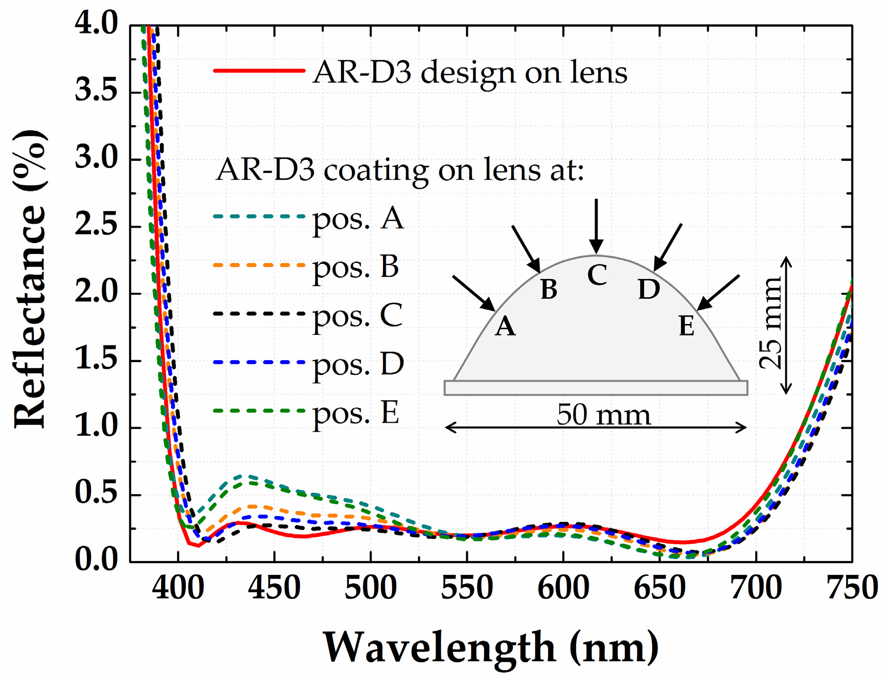
3.4. Antireflection Coating for an Aspheric Lens

To confirm that ALD AR-coatings can be also used to reduce reflection losses of larger lenses, a second antireflection coating was applied to a steeply curved aspheric lens with center height of 25 mm and a diameter of 50 mm. Ta2O5 was used as high-index material for the AR coating, since the grown Ta2O5 ALD thin films are amorphous and hence no additional Al2O3 interlayer is needed to inhibit crystal growth. TEM and SEM images of about 5 nm, 35 nm and 200 nm Ta2O5 thin films show an amorphous structure [33,44,45]. X-ray diffraction (XRD) measurements also confirmed the amorphous nature of 200 nm tanatala thin films grown from Ta(OEt)5 at 300 °C. These spectra are not shown here.
The glass lens has a refractive index that is similar to that of B270. An AR-D3 coating (see Table 4) was designed to reduce the reflectance of a B270 substrate from approximately 4.0% to less than 0.5% in the visible spectral range from 400 nm to 700 nm. The first part of the coating design is based on the patented AR-hard® (Jena, Germany). A thin high-index layer is sandwiched by two thicker lower-index layers forming a symmetrical stack of three-quarter-wave optical thickness [46]. Silicon dioxide was chosen as final layer to attain a low residual reflectance. After completion of the Al2O3/Ta2O5 sequences in the Sunale R200 tool at a deposition temperature of 300 °C, the samples were unloaded to atmosphere and transferred to the OpAL tool for further processing of the top SiO2 layer at 100 °C.
Figure 8 depicts the reflectance of the AR-D3 design and the AR-D3-coated lens. The reflectance spectra of the lens show a good match to the design. Minor deviations between design and the measured reflectance at the inclined surface of the lens (position A and E) may be attributed to a temperature gradient of the lens during deposition and to lateral thickness non-uniformity across the chamber.

4. Conclusions

Atomic layer deposition successfully applies to deposit antireflection coatings on strongly curved lenses. In particular, the average reflectance could be minimized to 0.3% for a fused silica half-ball lens with 4 mm diameter and a steeply curved B270 aspherical lens in the visible spectral range from 400 to 750 nm and 400 to 700 nm, respectively. Similar reflectance spectra across the entire lens surface at normal light incidence are a result of the very good conformality of ALD coatings. The good agreement between design and coatings confirms the precise thickness control of ALD thin films. Thickness monitoring was not necessary to reach the desired film thicknesses, but only the counting of ALD cycles. Moreover, it was demonstrated that the conformal deposition is not restricted to the radius of curvature of a lens, as an AR coating that was deposited simultaneously on both sides of a flat glass substrate showed identical spectra on both sides. Noteworthy, these antireflection coatings are demonstrated in two commercially available tools with significantly different configurations, indicating that ALD can become highly attractive for production purposes.
Further development of ALD coating equipment such as spatial ALD, atmospheric pressure ALD, and batch tools will increase the applicability of this technology for high volume applications. The slow deposition rate is considered as the main disadvantage of ALD. The long deposition times are generally the consequence of the required purge times between the precursor pulses. The possibility to perform double-sided coatings increases the throughput of this coating technology. Spatial ALD [47] is a promising approach to shorten the purge times, in that the substrate is moved to different precursor zones, hence precursor pulses are spatially separated and purge steps become dispensable. The use of batch coaters is another possibility to increase the throughput [16]. However, the lateral thickness uniformity needs to be improved for scale up to large-area. For a better uniformity, both the chamber design and the precursor chemistry needs to be improved. The development of precursors that are highly reactive and volatile, but at the same time thermally stable and non-corrosive, as well as the design of a tool, that comprises a uniform gas distribution, a homogeneous temperature and the absence of dead volumes remains a future challenge [39].
Although further research and developments are needed, ALD is a promising method to deposit optical thin films that can be prospectively applied for optical coatings on complex formed optical components due to the very good conformality of ALD coatings (convex and concave lenses, cylinders, ball lenses, etc.).

Acknowledgments

The research was supported by the Deutsche Forschungsgemeinschaft (DFG) (Emmy-Noether-Project SZ253/1-1) and the European Space Agency (ESA) (Contract No. 4000109161/13/NL/RA). This work was partially supported by the FhG Internal Programs under Grant No. Attract 066-601020. Kristin Pfeiffer thanks the Carl Zeiss Foundation for promoting her doctoral research studies. The authors gratefully acknowledge David Kästner for the micro-spectrophotometer measurements.

Author Contributions

Adriana Szeghalmi and Kristin Pfeiffer conceived and designed the experiments; Ulrike Schulz supported the design of the coatings; Kristin Pfeiffer performed the experiments, analyzed the data and wrote the paper. All authors critically revised the article.

Conflicts of Interest

The authors declare no conflict of interest.

References

  1. Raut, H.K.; Ganesh, V.A.; Nair, A.S.; Ramakrishna, S. Anti-reflective coatings: A critical, in-depth review. Energy Environ. Sci. 2011, 4, 3779. [Google Scholar] [CrossRef]
  2. Buskens, P.; Burghoorn, M.; Mourad, M.C.D.; Vroon, Z. Antireflective coatings for glass and transparent polymers. Langmuir 2016, 32, 6781–6793. [Google Scholar] [CrossRef] [PubMed]
  3. Hedayati, K.M.; Elbahri, M. Antireflective coatings: Conventional stacking layers and ultrathin plasmonic metasurfaces, a mini-review. Materials 2016, 9, 497. [Google Scholar] [CrossRef] [PubMed]
  4. Das, N.; Islam, S. Design and Analysis of nano-structured gratings for conversion efficiency improvement in GaAs solar cells. Energies 2016, 9, 690. [Google Scholar] [CrossRef]
  5. Pulker, H.K. Optical coatings deposited by ion and plasma pvd processes. Surf. Coat. Technol. 1999, 112, 250–256. [Google Scholar] [CrossRef]
  6. Thielsch, R.; Gatto, A.; Heber, J.; Kaiser, N. A comparative study of the UV optical and structural properties of SiO2, Al2O3, and HfO2 single layers deposited by reactive evaporation, ion-assisted deposition and plasma ion-assisted deposition. Thin Solid Films 2002, 410, 86–93. [Google Scholar] [CrossRef]
  7. Liu, C.; Kong, M.; Chun, G.; Gao, W.; Li, B. Theoretical design of shadowing masks for uniform coatings on spherical substrates in planetary rotation systems. Opt. Express 2012, 20, 23790. [Google Scholar] [CrossRef] [PubMed]
  8. Wang, Z.; West, P.R.; Meng, X.; Kinsey, N.; Shalaev, V.M.; Boltasseva, A. Angled physical vapor deposition techniques for non-conformal thin films and three-dimensional structures. MRS Commun. 2016, 6, 17–22. [Google Scholar] [CrossRef]
  9. Gross, M.; Dligatch, S.; Chtanov, A.C. Optimization of coating uniformity in an ion beam sputtering system using a modified planetary rotation method. Appl. Opt. 2011, 50, C316–C320. [Google Scholar] [CrossRef] [PubMed]
  10. Zhang, L.C.; Cai, X.K. Uniformity masks design method based on the shadow matrix for coating materials with different condensation characteristics. Sci. World J. 2013, 10, 160792. [Google Scholar] [CrossRef] [PubMed]
  11. Diao, Z.; Kraus, M.; Brunner, R.; Dirks, J.H.; Spatz, J.P. Nanostructured stealth surfaces for visible and near-infrared light. Nano. Lett. 2016, 16, 6610–6616. [Google Scholar] [CrossRef] [PubMed]
  12. Schulze, M.; Lehr, D.; Helgert, M.; Kley, E.B.; Tünnermann, A. Transmission enhanced optical lenses with self-organized antireflective subwavelength structures for the uv range. Opt. Lett. 2011, 36, 3924–3926. [Google Scholar] [CrossRef] [PubMed]
  13. Taylor, C.D.; Busse, L.E.; Frantz, J.; Sanghera, J.S.; Aggarwal, I.D.; Poutous, M.K. Angle-of-incidence performance of random anti-reflection structures on curved surfaces. Appl. Opt. 2016, 55, 2203–2213. [Google Scholar] [CrossRef] [PubMed]
  14. Riihelä, D.; Ritala, M.; Matero, R.; Leskelä, M. Introduction atomic layer epitaxy for the deposition of optical thin films. Thin Solid Films 1996, 289, 250–255. [Google Scholar] [CrossRef]
  15. Kumagai, H.; Toyoda, K.; Kobayashi, K.; Obara, M.; Iimura, Y. Titanium oxide aluminum oxide multilayer reflectors for ”water-window” wavelengths. Appl. Phys. Lett. 1997, 70, 2338–2340. [Google Scholar] [CrossRef]
  16. Maula, J. Atomic layer deposition for industrial optical coatings. Chin. Opt. Lett. 2010, 8, 53–58. [Google Scholar] [CrossRef]
  17. Li, Y.H.; Shen, W.D.; Zhang, Y.G.; Hao, X.; Fan, H.H.; Liu, X. Precise broad-band anti-refection coating fabricated by atomic layer deposition. Opt. Commun. 2013, 292, 31–35. [Google Scholar] [CrossRef]
  18. Li, Y.H.; Shen, W.D.; Hao, X.; Lang, T.T.; Jin, S.Z.; Liu, X. Rugate notch filter fabricated by atomic layer deposition. Appl. Opt. 2014, 53, A270–A275. [Google Scholar] [CrossRef] [PubMed]
  19. Pfeiffer, K.; Shestaeva, S.; Bingel, A.; Munzert, P.; Ghazaryan, L.; van Helvoirt, C.; Kessels, W.M.M.; Sanli, U.T.; Grévent, C.; Schütz, G.; et al. Comparative study of ALD SiO2 thin films for optical applications. Opt. Mater. Express 2016, 6, 660–670. [Google Scholar] [CrossRef]
  20. Szeghalmi, A.; Helgert, M.; Brunner, R.; Heyroth, F.; Gosele, U.; Knez, M. Atomic layer deposition of Al2O3 and TiO2 multilayers for applications as bandpass filters and antireflection coatings. Appl. Opt. 2009, 48, 1727–1732. [Google Scholar] [CrossRef]
  21. Shestaeva, S.; Bingel, A.; Munzert, P.; Ghazaryan, L.; Patzig, C.; Tünnermann, A.; Szeghalmi, A. Mechanical, structural, and optical properties of PEALD metallic oxides for optical applications. Appl. Opt. 2017, 56, C47–C59. [Google Scholar] [CrossRef] [PubMed]
  22. Ritala, M.; Niinistö, J. Atomic layer deposition. In Chemical Vapour Deposition: Precursors, Processes and Applications; Jones, A.C., Hitchman, M.L., Eds.; Royal Society of Chemistry: Cambridge, UK, 2009; pp. 158–206. [Google Scholar]
  23. Kariniemi, M.; Niinisto, J.; Vehkamaki, M.; Kemell, M.; Ritala, M.; Leskela, M.; Putkonen, M. Conformality of remote plasma-enhanced atomic layer deposition processes: An experimental study. J. Vac. Sci. Technol. A 2012, 30, 01A115. [Google Scholar] [CrossRef]
  24. Siefke, T.; Kroker, S.; Pfeiffer, K.; Puffky, O.; Dietrich, K.; Franta, D.; Ohlidal, I.; Szeghalmi, A.; Kley, E.B.; Tünnermann, A. Materials pushing the application limits of wire grid polarizers further into the deep ultraviolet spectral range. Adv. Opt. Mater. 2016, 4, 1780–1786. [Google Scholar] [CrossRef]
  25. Stenzel, O.; Wilbrandt, S.; Friedrich, K.; Kaiser, N. Realistische Modellierung der NIR/VIS/UV-optischen Konstanten dünner optischer Schichten im Rahmen des Oszillatormodells. Vak. Forsch. Prax. 2009, 21, 15–23. [Google Scholar] [CrossRef]
  26. Groner, M.D.; Fabreguette, F.H.; Elam, J.W.; George, S.M. Low-temperature Al2O3 atomic layer deposition. Chem. Mat. 2004, 16, 639–645. [Google Scholar] [CrossRef]
  27. Puurunen, R.L. Surface chemistry of atomic layer deposition: A case study for the trimethylaluminum/water process. J. Appl. Phys. 2005, 97, 121301. [Google Scholar] [CrossRef]
  28. Pfeiffer, K.; Schulz, U.; Tünnermann, A.; Szeghalmi, A. Ta2O5/Al2O3/SiO2—Antireflective coating for non-planar optical surfaces by atomic layer deposition. Proc. SPIE 2017, 10115, 1011513. [Google Scholar]
  29. Ghazaryan, L.; Kley, E.B.; Tünnermann, A.; Szeghalmi, A. Nanoporous SiO2 thin films made by atomic layer deposition and atomic etching. Nanotechnology 2016, 27, 255603. [Google Scholar] [CrossRef] [PubMed]
  30. Dingemans, G.; van Helvoirt, C.A.A.; Pierreux, D.; Keuning, W.; Kessels, W.M.M. Plasma-assisted ALD for the conformal deposition of SiO2: Process, material and electronic properties. J. Electrochem. Soc. 2012, 159, H277–H285. [Google Scholar] [CrossRef]
  31. Putkonen, M.; Bosund, M.; Ylivaara, O.M.E.; Puurunen, R.L.; Kilpi, L.; Ronkainen, H.; Sintonen, S.; Ali, S.; Lipsanen, H.; Liu, X.W.; et al. Thermal and plasma enhanced atomic layer deposition of SiO2 using commercial silicon precursors. Thin Solid Films 2014, 558, 93–98. [Google Scholar] [CrossRef]
  32. Ylivaara, O.M.E.; Liu, X.W.; Kilpi, L.; Lyytinen, J.; Schneider, D.; Laitinen, M.; Julin, J.; Ali, S.; Sintonen, S.; Berdova, M.; et al. Aluminum oxide from trimethylaluminum and water by atomic layer deposition: The temperature dependence of residual stress, elastic modulus, hardness and adhesion. Thin Solid Films 2014, 552, 124–135. [Google Scholar] [CrossRef]
  33. Kukli, K.; Ritala, M.; Leskelä, M. Atomic layer epitaxy growth of tantalum oxide thin films from Ta(OC2H5)5 and H2O. J. Electrochem. Soc. 1995, 142, 1670–1675. [Google Scholar] [CrossRef]
  34. Blanquart, T.; Longo, V.; Niinistö, J.; Heikkilä, M.; Kukli, K.; Ritala, M.; Leskelä, M. High-performance imido–amido precursor for the atomic layer deposition of Ta2O5. Semicond. Sci. Technol. 2012, 27, 074003. [Google Scholar] [CrossRef]
  35. Hausmann, D.M.; de Rouffignac, P.; Smith, A.; Gordon, R.; Monsma, D. Highly conformal atomic layer deposition of tantalum oxide using alkylamide precursors. Thin Solid Films 2003, 443, 1–4. [Google Scholar] [CrossRef]
  36. Zhao, C.; Hedhili, M.N.; Li, J.; Wang, Q.; Yang, Y.; Chen, L.; Li, L. Growth and characterization of titanium oxide by plasma enhanced atomic layer deposition. Thin Solid Films 2013, 542, 38–44. [Google Scholar] [CrossRef]
  37. Potts, S.E.; Kessels, W.M.M. Energy-enhanced atomic layer deposition for more process and precursor versatility. Coord. Chem. Rev. 2013, 257, 3254–3270. [Google Scholar] [CrossRef]
  38. Xie, Q.; Musschoot, J.; Deduytsche, D.; Vanmeirhaeghe, R.; Detavernier, C.; Van Den Berghe, S. Growth kinetics and crystallization behavior of TiO2 films prepared by plasma enhanced atomic layer deposition. J. Electrochem. Soc. 2008, 155, H688–H692. [Google Scholar] [CrossRef]
  39. Elers, K.E.; Blomberg, T.; Peussa, M.; Aitchison, B.; Haukka, S.; Marcus, S. Film uniformity in atomic layer deposition. Chem. Vap. Depos. 2006, 12, 13–24. [Google Scholar] [CrossRef]
  40. Miikkulainen, V.; Leskela, M.; Ritala, M.; Puurunen, R.L. Crystallinity of inorganic films grown by atomic layer deposition: Overview and general trends. J. Appl. Phys. 2013, 113, 021301. [Google Scholar] [CrossRef]
  41. Ratzsch, S.; Kley, E.B.; Tunnermann, A.; Szeghalmi, A. Influence of the oxygen plasma parameters on the atomic layer deposition of titanium dioxide. Nanotechnology 2015, 26, 024003. [Google Scholar] [CrossRef] [PubMed]
  42. Ylivaara, O.M.E.; Kilpi, L.; Liu, X.W.; Sintonen, S.; Ali, S.; Laitinen, M.; Julin, J.; Haimi, E.; Sajavaara, T.; Lipsanen, H.; et al. Aluminum oxide/titanium dioxide nanolaminates grown by atomic layer deposition: Growth and mechanical properties. J. Vac. Sci. Technol. A 2017, 35, 01B105. [Google Scholar] [CrossRef]
  43. Hoffmann, L.; Theirich, D.; Pack, S.; Kocak, F.; Schlamm, D.; Hasselmann, T.; Fahl, H.; Raupke, A.; Gargouri, H.; Riedl, T. Gas diffusion barriers prepared by spatial atmospheric pressure plasma enhanced ALD. ACS Appl. Mater. Interfaces 2017, 9, 4171–4176. [Google Scholar] [CrossRef] [PubMed]
  44. Szeghalmi, A.; Senz, S.; Bretschneider, M.; Gösele, U.; Knez, M. All dielectric hard X-ray mirror by atomic layer deposition. Appl. Phys. Lett. 2009, 94, 133111. [Google Scholar] [CrossRef]
  45. Mayer, M.; Grévent, C.; Szeghalmi, A.; Knez, M.; Weigand, M.; Rehbein, S.; Schneider, G.; Baretzky, B.; Schütz, G. Multilayer Fresnel zone plate for soft X-ray microscopy resolves sub-39 nm structures. Ultramicrospcopy 2011, 111, 1706–17011. [Google Scholar] [CrossRef] [PubMed]
  46. Schulz, U.; Schallenberg, U.B.; Kaiser, N. Symmetrical periods in antireflective coatings for plastic optics. Appl. Opt. 2003, 42, 1346–1351. [Google Scholar] [CrossRef] [PubMed]
  47. Poodt, P.; Cameron, D.C.; Dickey, E.; George, S.M.; Kuznetsov, V.; Parsons, G.N.; Roozeboom, F.; Sundaram, G.; Vermeer, A. Spatial atomic layer deposition: A route towards further industrialization of atomic layer deposition. J. Vac. Sci. Technol. A 2012, 30, 010802. [Google Scholar] [CrossRef]
Figure 1. Illustration of (a) physical vapor deposition (PVD) deposition and (b) atomic layer deposition (ALD) on a hemispherical lens.
Coatings 07 00118 g001
Figure 2. Thickness uniformity mapping of Al2O3 (thermal ALD) on a 200 mm wafer measured after (a) 1156 ALD cycles without rotation, (b) 1000 ALD cycles with manual sample rotation by 180° after 500 ALD cycles.
Coatings 07 00118 g002
Figure 3. Reflectance spectra of AR-D1 on fused silica reference glass substrate: (a) Design and coating; (b) Corrected design (with interlayer) and recalculation from measured spectra (taking the Al2O3 interlayer into account).
Coatings 07 00118 g003
Figure 4. Measured and expected reflectance spectra of AR-D2 on fused silica reference glass substrate positioned: (a) at the center of the substrate table; (b) at approximately 75 mm from the center table.
Coatings 07 00118 g004
Figure 5. (a) Measured reflectance spectra of uncoated fused silica reference glass substrate and uncoated fused silica half-ball lens; (b) Measured reflectance spectra (AOI = 0°) of AR-coated fused silica half-ball lens at different positions of the lens.
Coatings 07 00118 g005
Figure 6. Measured and expected reflectance spectra (AOI = 0°) of AR-D2 deposited simultaneously on both sides of an upright-positioned flat fused silica glass substrate.
Coatings 07 00118 g006
Figure 7. Measured and expected reflectance spectra (AOI = 0°) of AR-coated fused silica half-ball lens at different positions of the lens.
Coatings 07 00118 g007
Figure 8. Measured and expected reflectance spectra (AOI = 0°) of the AR-coated steeply curved B270 aspherical lens at different positions of the lens.
Coatings 07 00118 g008
Table 1. Process parameter for depositing SiO2, Al2O3, TiO2 and Ta2O5 ALD thin films.
MaterialPrecursor, Source Temperature, Delivery MethodOxidizing AgentALD ToolALD Cycle [Pulse/Purge/Gas Stabilization/Oxidizing Pulse/Purge] (in s)
SiO23DMAS, 30 °C, vapor drawO2-plasmaOpAL[0.4 + 4 (hold)/–/5/3/4]
Al2O3TMA, 20 °C, vapor drawO2-plasmaOpAL[0.04/3.5/2.5/5/3.5]
Al2O3TMA, 20 °C, vapor drawH2O2Sunale[0.1/4.0/–/0.2/4.0]
TiO2TTIP, 50 °C, bubblingO2-plasmaOpAL[1.5/7.0/3.0/6.0/4.0]
Ta2O5Ta(OEt)5, 185 °C, pressure boostH2O2Sunale[1.6/6.0/–/2.0/10]
Table 2. Growth rate on silicon substrates (growth per cycles (GPC) in Å/cycle), refractive index and thickness non-uniformity over a 200 mm area of deposited ALD thin films. The corresponding deposition temperatures are given in brackets.
Material/PropertiesSiO2 (100 °C)Al2O3 (100 °C)Al2O3 (300 °C)Ta2O5 (300 °C)TiO2 (100 °C)
ToolOpALOpALSunaleSunaleOpAL
GPC on Si1.201.210.890.490.29
n @ 550 nm1.461.621.662.212.44
NU% 1±1.5%±1.5%±2.1%±4.0%±2.0%
1 thickness non-uniformity, defined as NU% = (dmaxdmin)/2daverage × 100.
Table 3. Designed layer thickness and necessary ALD cycles of AR coating on fused silica.
MaterialAR-D1AR-D2
ExperimentalRecalculationExperimental
Design (nm)Coating (nm)ALD CyclesActual Thickness (nm)Actual GPC (Å/cycle)Design and Coating (nm)ALD Cycles
Al2O375.175.162175.41.2176.8635
TiO216.116.155616.10.2916.1555
Al2O320.520.517019.91.1721.5184
TiO263.933.3115032.50.2837.51293
Al2O31.5121.41.171.513
TiO230.6105431.00.2924.3837
Al2O313.213.210912.81.1714.1120
TiO225.0025.0086225.30.2924.2834
SiO292.392.376990.21.1792.7792
Table 4. Designed layer thickness and necessary ALD cycles of AR coating on B270.
MaterialAR-D3
Thickness (nm)ALD Cycles
Al2O3101.61181
Ta2O511.2208
Al2O3186.92173
Ta2O535.0714
Al2O321.8253
Ta2O543.6891
SiO293.7787

