Article

Highly-Conductive and Well-Adhered Cu Thin Film Fabricated on Quartz Glass by Heat Treatment of a Precursor Film Obtained Via Spray-Coating of an Aqueous Solution Involving Cu(II) Complexes

1
Applied Chemistry and Chemical Engineering Program, Graduate School, Kogakuin University, 2665-1 Nakano, Hachioji, Tokyo 192-0015, Japan
2
Department of Applied Physics, School of Advanced Engineering, Kogakuin University, 2665-1 Nakano, Hachioji, Tokyo 192-0015, Japan
*
Author to whom correspondence should be addressed.
Coatings 2018, 8(10), 352; https://doi.org/10.3390/coatings8100352
Submission received: 21 August 2018 / Revised: 27 September 2018 / Accepted: 28 September 2018 / Published: 2 October 2018

Abstract

:
A Cu thin film on a quartz glass substrate was fabricated by a wet process involving heat-treatment of a precursor film spray-coated with an aqueous ammonia solution containing Cu(HCOO)2∙4H2O and Cu(II) complex of ethylenediamine-N,N,N′N′-tetraacetic acid. The precursor film that formed on the substrate at 180 °C in air was heat-treated at 350 °C and post annealed at 400 °C by placing an identical-sized glass on top, under Ar gas flow in a tubular furnace. X-ray diffraction pattern of the resultant film showed only peaks of Cu. The resultant film of 100 nm thickness has an adhesion strength and electrical resistivity of 37(7) MPa and 3.8(6) × 10−5 Ω cm, respectively. The images of atomic force and field-emission scanning-electron microscopies revealed a film of well-connected Cu grains with an average surface roughness of 11 nm. The reflectance of the thin film is more than 90% in the far-infrared region. The film’s chemical composition was also examined by using Auger electron spectroscopy.

1. Introduction

Cu is an important metallic material due to its excellent electrical conductivity, only second to silver but more abundant and affordable. Therefore, thin films of metallic Cu have been identified as promising conductive materials and extensively used in microelectronics [1]. Leading techniques, such as radio-frequency sputtering [2] and chemical vapor deposition [3], have been found to be capable of depositing Cu thin films of good quality. However, the high cost, complicated experimental setups and procedures associated with these techniques [4], make it impossible for an effective and low-cost fabrication of Cu thin films. Although electroless plating is another promising technology for the deposition of Cu thin films especially on insulating substrates, the use of PdCl2 and SnCl2 to activate the surface of the specimens compromises the quality of the thin films [5]. The use of inks containing Cu nanoparticles is also a promising technique for fabricating Cu films, usually of several microns in thickness and this research area is very active [6,7,8]. The multiple steps required in preparing the Cu nanoparticles, protecting them against oxidation using capping agents and finding appropriate solvents to obtain suitable inks still remain as some of the challenging aspects.
The molecular precursor method (MPM) is an effective, wet chemical process for thin film fabrication of various metal oxides and phosphates that was developed in our laboratory [9]. The fabrication of a conductive and semi-transparent Cu thin film using MPM was recently reported [10]. Additionally, a highly conductive and void-free metallic Cu thin-film was successfully embedded into submicrometer trenches in a silicon substrate using a modified molecular precursor solution [11]. In the fabrication of these thin films by the MPM, metal complexes are dissolved in ethanol by combining them with appropriate alkylamines, and this yields good coating solutions with excellent stability, homogeneity, miscibility and coatability.
The use of volatile organic compound (VOC)-free solutions in the MPM was recently reported by our group [12]. In the work, the fabrication of a biocompatible carbonated-apatite film adhered onto a titanium plate was achieved by spray-coating an aqueous solution involving a carbonated-apatite precursor. From the environmental safety point of view, aqueous-based solutions are preferred over alcohol-based solutions [13]. Spray-coating is an emerging solution-based coating technique and its applications have been well established in graphic arts, industrial coatings and paintings [14] and the fabrication of thin films of various organic/polymer compounds [15], metal oxides [16] and metal sulfides [17] has been reported. The technique benefits from its relatively simple and inexpensive instrumentation set-up, reduced material losses [18], ability to be adjusted for large area deposition and produce thin films in a Roll-to-Roll and high throughput process in comparison to other solution-based techniques such as spin coating [19]. We here report the fabrication of a highly conductive Cu thin film from aqueous solutions involving Cu(II) complexes, under ambient conditions via the MPM. The fabrication of metallic Cu thin films via wet chemical processes employing aqueous solutions, such as the spray method has not been reported yet, as far as we know.

2. Materials and Methods

2.1. Materials

Ethylenediamine-N,N,N,N′-tetraacetic acid (EDTA, C10H16N2O8) and Cu(II) acetate monohydrate (Cu(CH3COO)2∙H2O) were purchased from Kanto Chemical Co., Inc. (Tokyo, Japan). Cu(II) formate tetrahydrate (Cu(HCOO)2∙4H2O) was purchased from Wako Pure Chemical Industries, Ltd. (Osaka, Japan) Concentrated aqueous ammonia (NH4OH, 28 wt %) was purchased from Taisei Chemical Co., Ltd. (Tokyo, Japan). Deionized water was purchased from Kyoei Pharmaceuticals Co., Ltd. (Chiba, Japan). All chemicals were used without further purification. Quartz glass substrate with dimensions 100 × 100 × 1.6 mm3 (purchased from Akishima Glass Co., Ltd., Tokyo, Japan) was cut into 20 × 20 mm2 and ultrasonically cleaned with a water-detergent mixture for 0.5 h, rinsed several times with deionized water and finally with 2-propanol.

2.2. Preparation of the Coating Solutions

Two different solutions were prepared and the [Cu(H2edta)]∙H2O complex was isolated according to the procedures previously reported [20]. The coating solutions were prepared as follows: The coating solution Sedta was prepared by mixing [Cu(H2edta)]∙H2O (0.980 g, 2.63 mmoL) with 28% NH4OH (0.360 g, 5.90 mmoL NH3) in 25 g of deionized water. The mixed solution Smix was prepared by mixing [Cu(H2edta)]∙H2O (0.20 g, 0.53 mmoL) with Cu(HCOO)2∙4H2O (0.48 g, 2.11 mmoL) in 25 g of deionized water, followed by the addition of 28% NH4OH (0.64 g, 10.5 mmoL NH3). The solutions were stirred on a magnetic stirrer for 1 h at room temperature, filtered through a 0.8 µm membrane filter and used with no further modifications.

2.3. Thin Film Fabrication

2.3.1. Spray-Coating

The spray-coating onto a pre-heated quartz glass substrate of 20 × 20 mm2 size was separately performed using abovementioned two coating solutions, using the identical experimental set-up used in the previous work [12]. The quartz glass was placed on a steel plate on top of a hot-plate. The temperature of the steel plate was kept at 180 °C and continuously monitored with a thermocouple (chromel-alumel type, surface probe A3-K-1-Q, TGK, Tokyo, Japan). Each coating solution (6 mL) was sprayed onto the pre-heated substrate from the airbrush (HP-SAR; ANEST IWATA Co., Kanagawa, Japan) using compressed air (0.2 MPa) as a carrier gas, spraying for 5 s at 20 s intervals and at a spray rate of 1.67 mL min–1. The vertical distance between the tip of the airbrush and the substrate was 30 cm. The obtained films are denoted as Fedta and Fmix, fabricated using the coating solutions Sedta and Smix, respectively.

2.3.2. Heat-Treatment of the Spray-Coated Film

The films, Fedta and Fmix were heat-treated at 350 °C for 50 min under Ar gas with a flow rate of 1.5 L min−1 in a tubular furnace (EPKRO-12K, Isuzu, Tokyo, Japan) with a quartz glass tube (40 mm diameter and 650 mm length). The tube was filled with Ar gas by purging air for 10 min at a flow rate of 1.5 L min−1. The furnace was heated to 350 °C from 25 °C at a constant temperature raising rate of 14 °C min–1, kept at 350 °C for 50 min and then cooled to room temperature. The resultant films obtained by heat-treating Fedta and Fmix are denoted as F’edta and F’mix, respectively. The heat-treated films were post-annealed by placing a clean identical-sized quartz glass on top and heat-treating at 400 °C for 50 min under an Ar gas at a flow rate of 1.5 L min−1, in the same tubular furnace. Hereafter, the resultant films obtained from the post-annealing of F’edta and F’mix are denoted as F’’edta and F’’mix, respectively.

2.4. Measurements

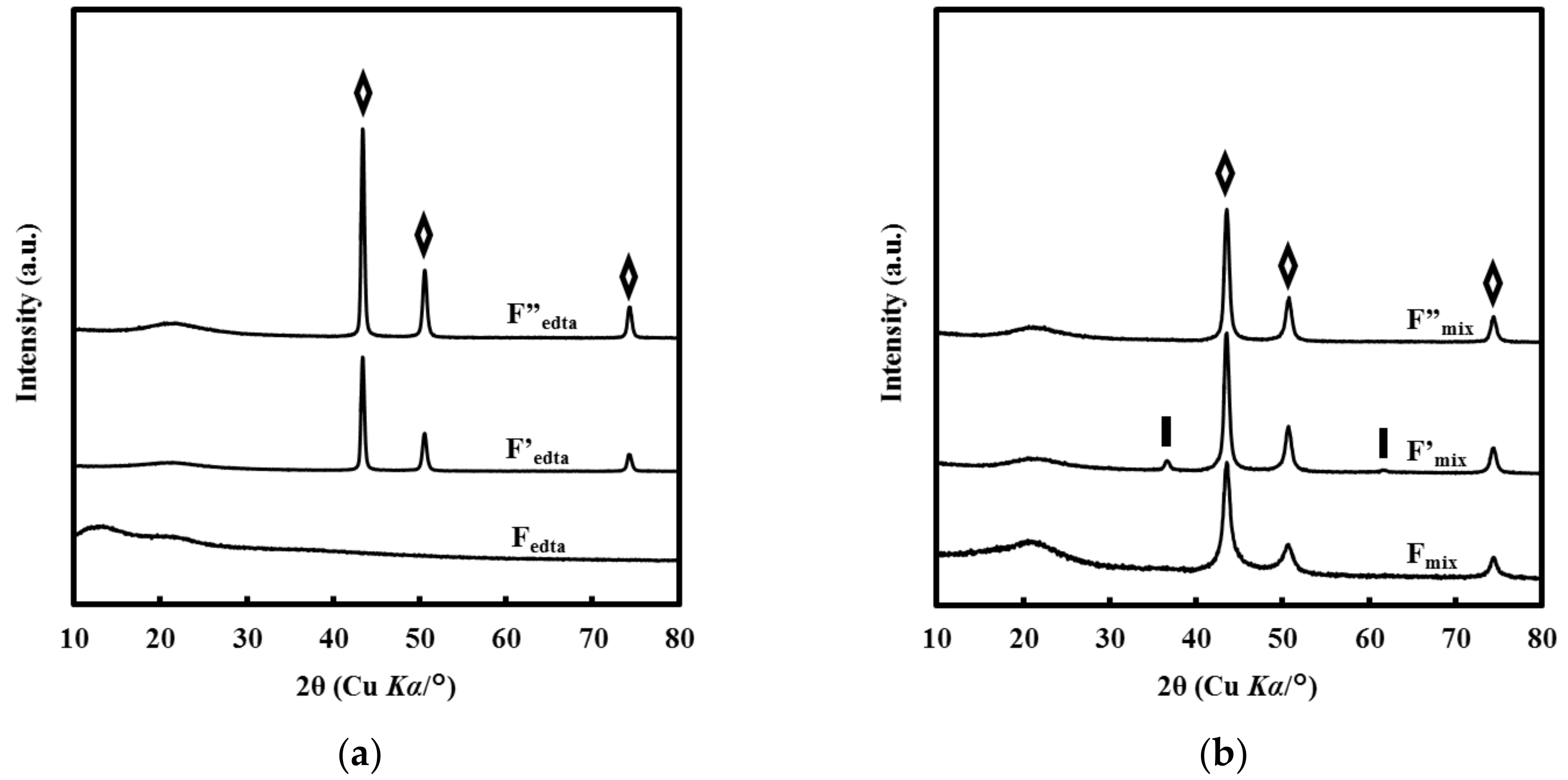
2.4.1. Crystal Structure of the Films

The crystal structures of all films were determined by means of X-ray diffraction (XRD) using a SmartLab X-ray diffractometer (Rigaku, Tokyo, Japan) with Cu Kα radiation-source at a power of 45 kV and 200 mA. Parallel beam optics at an incidence angle 0.3° was used in the 2θ range of 10°–80°, scanning at 0.05° step width and a speed of 5° min−1.

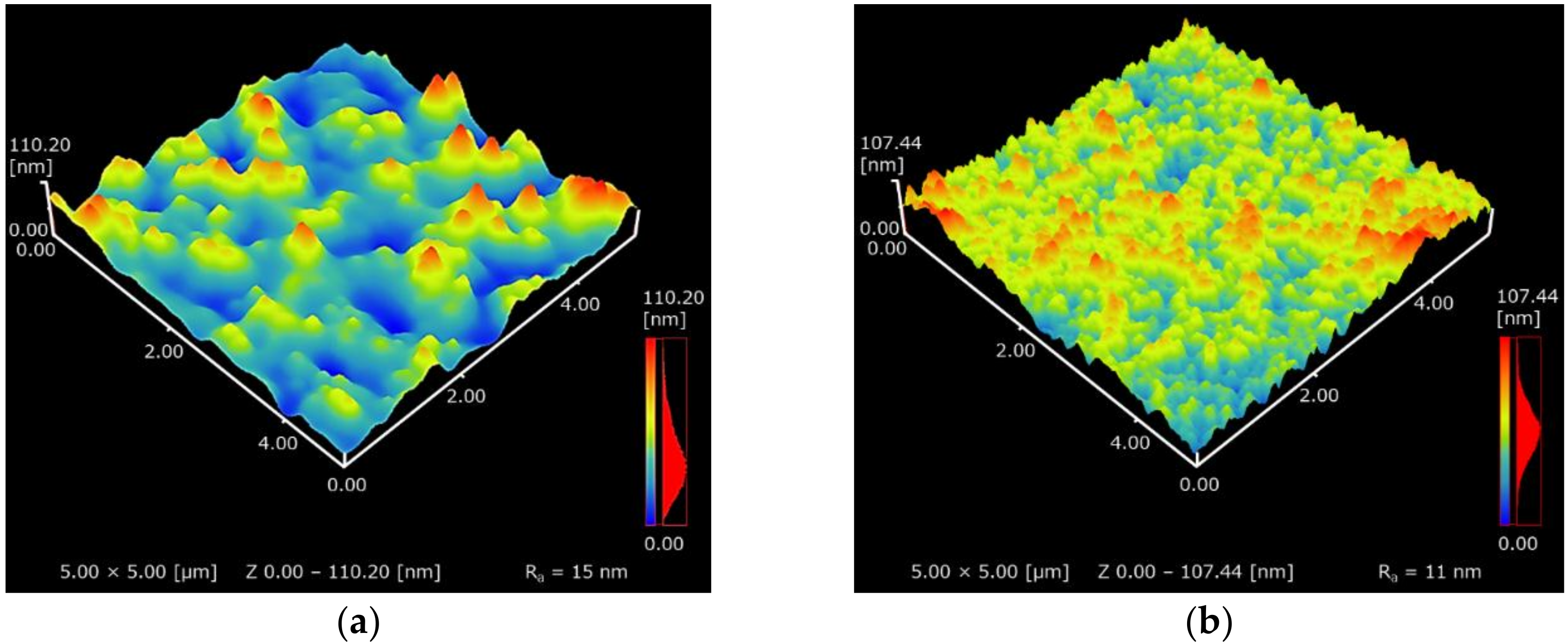
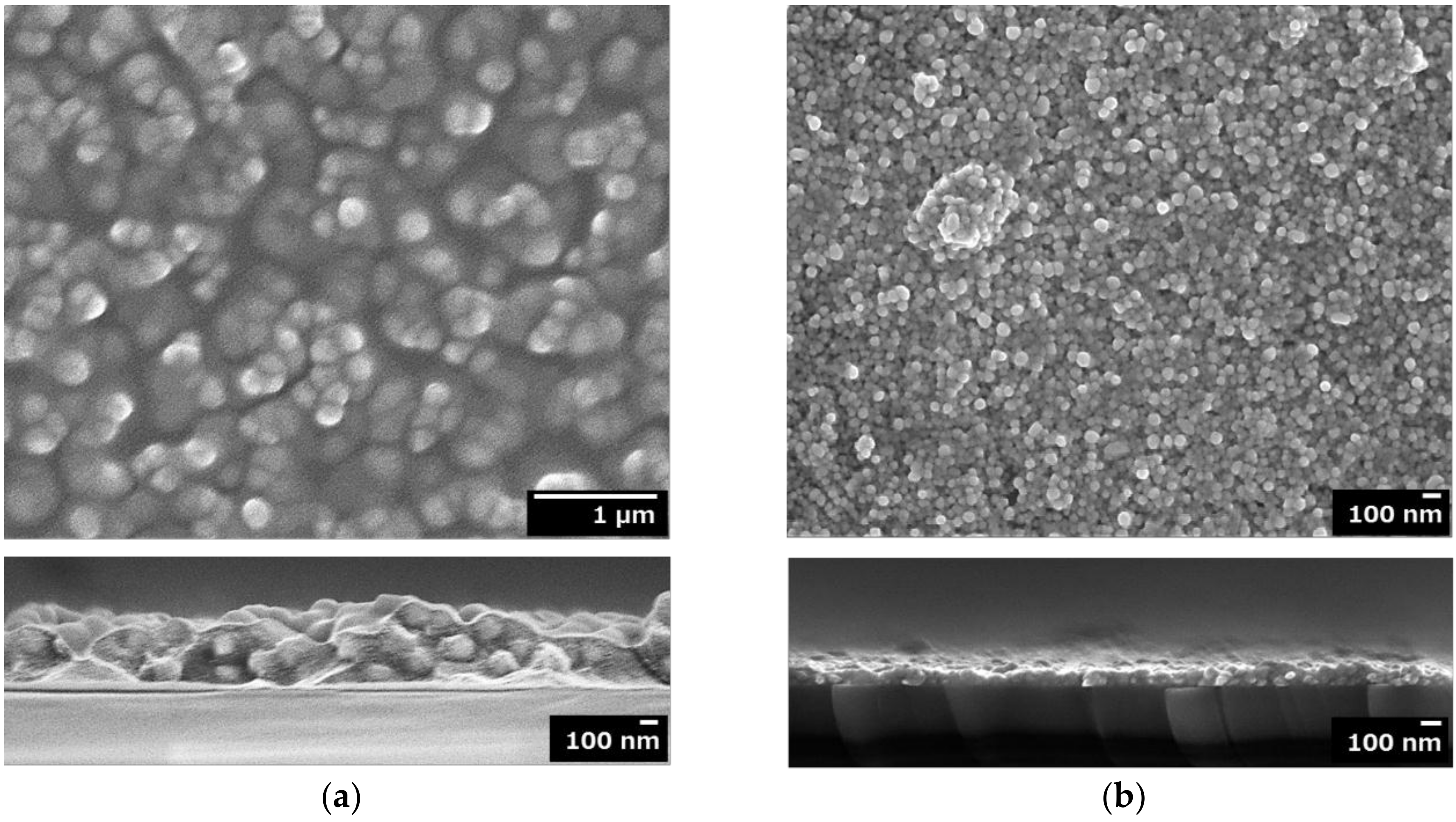
2.4.2. Surface Morphologies of F’’edta and F’’mix and Adhesion Strength of F’’mix

The surface 3D views of F’’edta and F’’mix were obtained by atomic force microscopy (AFM) using a LEXT OLS3500/SFT-3500 (Olympus Inc., Tokyo, Japan) by scanning each 5 × 5 μm2 area. The surface morphologies of F’’edta and F’’mix were also observed by field-emission scanning electron microscopy (FE-SEM) using a JSM-6701F (JEOL, Tokyo, Japan) at an accelerating voltage of 5 kV. The thickness of F’’mix was calculated as the average of ten different points taken from the cross-sectional SEM image.
The adhesion strength of F’’mix onto the substrate was tested by the stud-pull coating adhesion test. A stand pin, P/N901106 with an internal diameter of 2.7 mm was attached to the film with epoxy glue and set in an oven at 150 °C for 1 h. The test was then performed by pulling the stand pin with a load of 0 to 100 kg at a rate of 2.0 kg s–1.

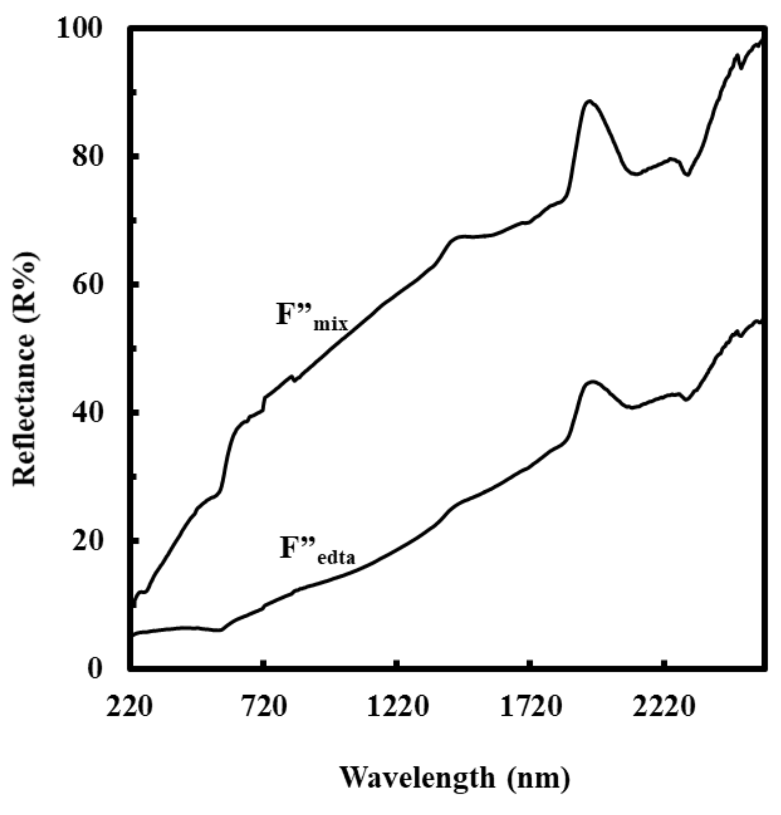
2.4.3. Reflectance Spectra of F’’edta and F’’mix and Electrical Resistivity of F’’mix

The reflectance spectra of F’’edta and F’’mix were measured with a UV-3600 spectrophotometer (SHIMADZU, Kyoto, Japan). The measurements were done in the 220–2600 nm range using a double beam mode and air as the reference.
The electrical resistance of F’’mix was evaluated using the four-probe method at 25 °C. The four-probe set-up consisted of a regulated DC power supply (Model PAB32-1.2, Kikusui Electronics Corp., Kanagawa, Japan), two multimeters (VOAC7512, Iwatsu (Tokyo, Japan) and Model 2010, Keithley, (Tokyo, Japan) as a current source and voltmeter, respectively) and four Au-plated tungsten probes placed at intervals of 1 mm (FELL type, K&S, Tokyo, Japan) with an added load of 0.1 kg.

2.4.4. Chemical Composition of F’’mix

The chemical composition of F’’mix was analyzed by means of Auger electron spectroscopy (AES) using a field emission Auger microprobe, JAMP-9500F (JEOL, Tokyo, Japan) with a probe voltage and current of 10 kV and 10 nA, respectively. The sample was cleaned by slightly etching a 100 μm area with an Ar+ beam (1000 eV, 10 nA, 30 s). The state of carbon present in the thin film was determined by curve-fitting of the carbon (CKLL) curve of F’’mix with those of neutral and tetravalent carbon.

3. Results

3.1. Crystal Structures of the Films

Figure 1a presents the XRD patterns of Fedta, F’edta and F’’edta. It was clarified that the film Fedta is amorphous, because no peak was observed in its pattern. The three peaks at 43.4°, 50.5° and 74.2° for both F’edta and F’’edta are assignable to the (111), (200) and (220) crystal phase of metallic Cu, respectively (ICDD card no. 00-004-0836).
In Figure 1b, the XRD patterns of Fmix, F’mix and F’’mix are given. In all patterns, the three peaks at 43.5°, 50.6° and 74.3° are assignable to the (111), (200) and (220) crystal phase of metallic Cu, respectively. In the XRD pattern of F’mix, two additional peaks assignable to the (111) and (220) crystal phase of Cu2O can be observed at 36.6° and 61.6°, respectively (ICDD card no. 01-071-3645).

3.2. Surface Morphologies of F’’edta and F’’mix and Adhesion Strength of F’’mix

The 3D AFM images of F’’edta and F’’mix are presented in Figure 2. The 3D image of F’’edta (Figure 2a) shows few, large and isolated grains. On the other hand, many, small and connected grains can be observed on the 3D image of F’’mix (Figure 2b). The average surface roughness was determined to be 15 nm and 11 nm for F’’edta and F’’mix, respectively.
The FE-SEM images of the F’’edta and F’’mix films are given in Figure 3a,b, respectively. From the top view of F’’edta, isolated agglomerates can be observed. These agglomerates can also be observed in the cross-sectional image. In Figure 3b, a crack-free surface with well-connected and closely packed Cu grains can be observed from the top view of F’’mix. The cross-sectional image reveals that the thin film is homogeneously and densely deposited on the quartz glass substrate.
The adhesion strength of the film F’’mix onto the quartz glass substrate was found to be 37(7) MPa.

3.3. Reflectance Spectra of F’’edta and F’’mix and Electrical Resistivity of F’’mix

Figure 4 shows the reflectance spectra of the resultant films. The reflectance of F’’mix approaches over 90% in the far infrared region while that of F’’edta approaches a maximum of 50% in the identical region. The thin film F’’mix has an electrical resistivity of 3.8(6) × 10−5 Ω cm, which was calculated by using the film thickness of 100 nm.

3.4. Chemical Composition of F’’mix

The AES spectrum of F’’mix are presented in Figure 5a. The surface scan indicated that the thin film is composed of C and Cu, as has been confirmed by one peak at 265 eV assignable to electrons of carbon atom and three peaks (LVV) at 764 eV, 835 eV and 914 eV assignable to electrons of Cu ones, respectively. Curve-fitting result (Figure 5b) revealed that all carbon atom present in the thin film is neutral.

4. Discussion

4.1. Preparation and Properties of the Precursor Solution

The stable and VOC-free solution Smix, which can be stored for a period of over three months, for fabricating the precursor film of metallic Cu was successfully developed by mixing [Cu(H2edta)] and Cu(II) formate with ammonia, in water. The aqueous solution was adequate for spraying onto a quartz glass substrate pre-heated to 180 °C, without forming the clogging solid in the nozzle tip. The abovementioned two-step heat-treatment of the sprayed film obtained in a short time produced a crack-free and densified film F’’mix of 100 nm thickness (Figure 2b and Figure 3b) with very low electrical resistivity and strong adhesion onto the substrate. It is important to point out that the precursor solution with a 1:4 of [Cu(edta)]:Cu(II) formate ratio reported here gave the best results with a good reproducibility, among several attempts with varying the ratios.
In spray pyrolysis works, the fabrication of Cu2O thin films onto alkali-free borosilicate, silicon and quartz glass substrates from aqueous solutions involving Cu(II) acetate requires the addition of glucose to act as reducing agent [21,22]. In their study, Kosugi and Kaneko outlined that the Cu2+ derived from Cu(II) acetate is reduced by glucose to form Cu0 which is subsequently oxidized to form Cu2O. It is also important to note that the properties of the film with Cu0 crystal phase obtained via the spray pyrolysis have not been reported. Thus, this present study is the first report on the fabrication of metallic Cu thin films via the spray-coating or any related aqueous solution-based techniques.

4.2. Influence of the Cu(II) Complexes in the Coating Solution on the Crystal Structure of the Resultant Films

In this study, it was established that spray-coating an aqueous solution of the Cu(II) complex of EDTA only, onto a quartz glass substrate preheated to 180 °C gives an amorphous film, Fedta (Figure 1a). However, under identical conditions as abovementioned, Fmix with crystallized Cu0 phase (Figure 1b) could be fabricated using a mixed solution of [Cu(H2edta)] and Cu(II) formate. These results suggest the importance of the used Cu(II) complexes involved in the coating solution. When the solution is made up of the large and stable complex only, such as in the case of Sedta, the preheating temperature of the substrate at 180 °C does not induce the nucleation of Cu0 grains on the substrate and the amorphous product is deposited instead. In this case, the nucleation and aggregation of Cu0 grains occur simultaneously during the heat-treating procedure at higher temperatures. This reaction process could be modified by using a mixed solution whereby the smaller Cu(II) complexes, for example [Cu(NH3)4]2+, derived from Cu(II) formate and ammonia in the solution promote nucleation of Cu0 grains during the spray-coating procedure. Because a network of Cu0 grains has been already formed in the sprayed film Fmix, the thermal decomposition of complexes during the heat-treating procedure leads to the densification of these grains resulting in a conductive thin film of well-connected Cu0 grains.

4.3. Influence of the Cu(II) Complexes in the Coating Solution on the Surface Morphologies, Electrical Conductivities and Reflectance of the Resultant Films

The reflectance and electrical resistivity are quite different between F’’edta and F’’mix. It is known that the formation of island shapes in metal films causes a decrease in the reflectance and electrical conductivity [23]. The insulating thin film F’’edta has island-shape features on the surface, whereas grains in F’’mix are well-connected as shown by their corresponding 3D AFM and top view SEM images (Figure 2 and Figure 3, respectively). It is important to note that the morphologies of F’’edta were only observable after sputtering the samples with a thin layer of gold. It is easily acceptable that the high degree of connectivity between the Cu0 grains promoted the very low electrical resistivity of F’’mix, whose value is 3.8(6) × 10–5 Ω cm. The bulk electrical resistivity of Cu is 1.67 × 10⁻⁶ Ω cm. However, the fabrication of Cu thin films with electrical resistivity values in the order of 10–5 Ω cm, via radio-frequency sputtering or atomic layer deposition have been reported [2,24,25]. Although it is not appropriate to directly compare these values due different fabrication conditions, the electrical resistivity of the thin film fabricated in the present study is acceptable. It is however important to note that contaminants at grain boundaries, which could not be determined by XRD, SEM and AES, may cause a decrease in the conductivity of the thin film formed by stacking of pure Cu grains.
It is notable that the reflectance of F’’mix approaches over 90% in the far-infrared region (Figure 4). In our previous work [10], we reported the fabrication of a Cu thin film, whose reflectance approaching nearly 100% in the identical region, with a thickness of 100 nm and an electrical resistivity of 1.8 × 10⁻⁵ Ω cm. The thin film was fabricated by a spin coating of an ethanol solution and two-step heat treatment. This present thin film F’’mix fabricated via spray-coating of aqueous solution can also be useful as an excellent reflector in the far-infrared region.

4.4. Chemical Composition and Adhesion-Strength of F’’mix

The AES spectrum (Figure 5a) revealed that in addition to Cu, the thin film F’’mix contains a certain amount of neutral carbon atoms, uniformly distributed within the film (Figure 5b). Consequently, these carbon atoms caused no disruption in the electrical conductivity and reflectance of the thin film. In our report on embedding Cu into submicrometer trenches in a silicon substrate [11], relative concentrations indicated that the trenches had a Cu:O:C ratio of 84:4:12 and this higher carbon content in comparison to oxygen might be useful in protecting the Cu from oxidation. Therefore, the thin film F’’mix is also likely to be resistant to oxidation. In fact, even though spray-coating was performed in air, the Cu0 phase in Fmix was effectively protected against oxidation as indicated by the XRD pattern (Figure 1b). A certain amount of Cu2O appeared as a by-product during heat-treatment at 350 °C carried out under Ar gas containing less than 10 ppm of air as its impurity, in our previous study [26]. The ratio of Cu2O:Cu peaks assignable to the (111) phase in that film right after the heat treatment was 57:43. In the present study, a Cu2O phase was also detected at the corresponding stage (F’mix, Figure 1b) and the corresponding ratio was 4:96, indicating significant difference. It can be concluded that this must be owing to the different ratios of the number of used ligands. On the basis of our previous procedures, the post-annealing step by placing an identical-sized quartz glass on top of the thin film was vital for the removal of the Cu2O phase by utilizing the carbons remaining within the film and preventing the introduction of oxygen from less than 10 ppm air contained as an impurity in the industrially available Ar gas. This is evident from the XRD patterns of F’mix and F’’mix (Figure 1b). The effectiveness of carbon atoms derived from the ligands in protecting the film against oxidation is also shown in this present study.
The applicability of conductive thin films across various fields depends strongly on their mechanical properties such as the adhesion strength onto the substrate [27]. It is important to note that the thin film F’’mix has a strong adhesion strength up to 37 MPa onto the quartz glass substrate. In our previous work, the thin film prepared from the precursor solution had an adhesion strength of 36 MPa whereas another film prepared using ion-beam assisted deposition attained an adhesion strength of 1.7 MPa [10]. There are various techniques utilized to modify the surface of substrates in order to promote excellent adhesion strength of thin films and a thin film of copper with an adhesion strength of 34 MPa onto an alumina substrate was fabricated via magnetron sputtering but only after pre-treatment of the substrate with an Ar gas plasma [28]. However, in techniques such as physical vapor deposition (PVD), it has been established that a good adhesion can be obtained as a result of the formation of a transition layer between the substrate and thin film [29]. Therefore, the strong adhesion of F’’mix onto the quartz substrate is expected to be a result of the interface having bonds between Cu and the O2– belonging to the quartz glass substrate, without any chemical or physical modification of the substrates’ surface.

4.5. Versatility of MPM in Cu Thin Film Fabrication

The crystallized thin film fabrication by the MPM is based on the redox reaction of the precursor complexes during heat-treatment of the precursor film [9]. The mechanism leading to the Cu0 thin film formation from the spin-coated precursor film involving Cu(II) complexes was investigated in our previous studies, by using an ethanol solution [10,30]. In the present study, we used aqueous solutions involving the identical raw materials, [Cu(H2edta)] and Cu(II) formate, though the used ratio of the Cu(II) species differs from each other.
In preparations of the precursor solutions, the ratio of the Cu(II) complexes in our previous and present report was 1:7 and 1:4 for [Cu(edta)]:Cu(II) formate, respectively. Therefore, it is clearly understandable that the content of organic materials derived from EDTA complex is higher in the present Fmix than in that of our previous study. Also in the present study, post-annealing under the identical condition produced the F’’mix thin film having excellent properties comparable to those of the previous study. These results show that the ratio of the raw materials was adequate to this present coating procedure. Thus, the MPM is versatile to regulate the ratios of metal complexes in the precursor solutions suitable for different coating techniques.

5. Conclusions

The fabrication of a Cu thin film was achieved by the use of an aqueous coating solution containing Cu(II) complexes, via a rather simple spray-coating procedure at ambient laboratory conditions for the first time. With a thickness of 100 nm, the fabricated thin film has a low electrical resistivity of 3.8(6) × 10–5 Ω cm and it is well-adhered onto the quartz glass substrate with an adhesion strength of 37 MPa.
By this present study, the importance of designing and mixing different Cu(II) complexes involved in the solution in order to control the crystal structure and surface morphology of the resultant film was clearly illustrated. By varying the ratio of the Cu(II) complexes in the coating solution, films with different crystal structures, morphologies and electrical properties could be obtained. And this is the advantage of the MPM which enables to design metal complexes in coating solutions, at the molecular level.
The spray method employing this aqueous precursor solution has the potential as a promising technique for the fabrication of metallic Cu thin films for various applications. From the environmental friendliness point of view, the use of aqueous solutions is of a great advantage for the industrial handling safety.

Author Contributions

Conceptualization, P.N.H., H.N. and M.S.; Methodology, P.N.H., H.N. and M.S.; Investigation, P.N.H., M.M. and T.S.; Writing-Original Draft Preparation, P.N.H.; Writing-Review & Editing, P.N.H., H.N., T.S. and M.S.; Supervision, H.N. and M.S.

Funding

This research received no external funding.

Acknowledgments

This work was supported by the Ministry of Education, Culture, Sports, Science and Technology of Japan (MEXT) through its Supported Program for the Strategic Research Foundation at Private Universities.

Conflicts of Interest

The authors declare no conflict of interest.

References

  1. Ghotbi, M.Y.; Rahmati, Z. Nanostructured copper and copper oxide thin films fabricated by hydrothermal treatment of copper hydroxide nitrate. Mater. Des. 2015, 85, 719–723. [Google Scholar] [CrossRef]
  2. Lee, S.; Kim, J.Y.; Lee, T.-W.; Kim, W.-K.; Kim, B.-S.; Park, J.H.; Bae, J.-S.; Cho, Y.C.; Kim, J.; Oh, M.-W.; et al. Fabrication of high-quality single-crystal Cu thin films using radio-frequency sputtering. Sci. Rep. 2015, 4, 6230. [Google Scholar] [CrossRef] [PubMed]
  3. Gordon, P.G.; Kurek, A.; Barry, S.T. Trends in Copper Precursor Development for CVD and ALD Applications. ECS J. Solid State Sci. Technol. 2015, 4, N3188–N3197. [Google Scholar] [CrossRef]
  4. Kaelin, M.; Zogg, H.; Tiwari, A.N.; Wilhelm, O.; Pratsinis, S.E.; Meyer, T.; Meyer, A. Electrosprayed and selenized Cu/In metal particle films. Thin Solid Films 2004, 457, 391–396. [Google Scholar] [CrossRef]
  5. Han, S.; Lee, T.L.; Yang, C.J.; Shih, H.C. Trench gap-filling copper by ion beam sputter deposition. Mater. Chem. Phys. 2006, 97, 19–22. [Google Scholar] [CrossRef]
  6. Abhinav, K.V.; Rao, R.V.K.; Karthik, P.S.; Singh, S.P. Copper conductive inks: Synthesis and utilization in flexible electronics. RSC Adv. 2015, 5, 63985–64030. [Google Scholar] [CrossRef]
  7. Park, B.K.; Kim, D.; Jeong, S.; Moon, J.; Kim, J.S. Direct writing of copper conductive patterns by ink-jet printing. Thin Solid Films 2007, 515, 7706–7711. [Google Scholar] [CrossRef]
  8. Magdassi, S.; Grouchko, M.; Kamyshny, A. Copper Nanoparticles for Printed Electronics: Routes towards Achieving Oxidation Stability. Materials 2010, 3, 4626–4638. [Google Scholar] [CrossRef] [PubMed]
  9. Nagai, H.; Sato, M. Heat Treatment in Molecular Precursor Method for Fabricating Metal Oxide Thin Films. In Heat Treatment: Conventional and Novel Applications; Czerwinski, F., Ed.; IntechOpen: London, UK, 2012. [Google Scholar] [Green Version]
  10. Nagai, H.; Mita, S.; Takano, I.; Honda, T.; Sato, M. Conductive and semi-transparent Cu thin film fabricated using molecular precursor solutions. Mater. Lett. 2015, 141, 235–237. [Google Scholar] [CrossRef]
  11. Nagai, H.; Suzuki, T.; Nakano, T.; Sato, M. Embedding of copper into submicrometer trenches in a silicon substrate using the molecular precursor solutions with copper. Mater. Lett. 2016, 182, 206–209. [Google Scholar] [CrossRef]
  12. Mochizuki, C.; Hara, H.; Takano, I.; Hayakawa, T.; Sato, M. Application of carbonated apatite coating on a Ti substrate by aqueous spray method. Mater. Sci. Eng. C 2013, 33, 951–958. [Google Scholar] [CrossRef] [PubMed]
  13. Singh, I.; Bedi, R.K. Studies and correlation among the structural, electrical and gas response properties of aerosol spray deposited self assembled nanocrystalline CuO. Appl. Surf. Sci. 2011, 257, 7592–7599. [Google Scholar] [CrossRef]
  14. Girotto, C.; Rand, B.P.; Genoe, J.; Heremans, P. Exploring spray coating as a deposition technique for the fabrication of solution-processed solar cells. Sol. Energy Mater. Sol. Cells 2009, 93, 454–458. [Google Scholar] [CrossRef]
  15. Abdellah, A.; Baierl, D.; Fabel, B.; Lugli, P.; Scarpa, G.; München, T.U. Spray-coating deposition for large area organic thin-film devices. NSTI-Nanotech 2009, 2, 447–450. [Google Scholar]
  16. Muhibbullah, M.; Hakim, M.O.; Choudhury, M.G.M. Studies on Seebeck effect in spray deposited CuO thin film on glass substrate. Thin Solid Films 2003, 423, 103–107. [Google Scholar] [CrossRef]
  17. Yamamoto, A.; Nakamura, M.; Seki, A.; Li, E.L. Pyrite (FeS2) thin films prepared by spray method. Sol. Energy Mater. Sol. Cells 2003, 75, 451–456. [Google Scholar] [CrossRef]
  18. Khim, D.; Baeg, K.; Yu, B.; Kang, S.; Kang, M. Spray-printed organic field-effect transistors and complementary inverters. J. Mater. Chem. C 2013, 1, 1500–1506. [Google Scholar] [CrossRef]
  19. Eslamian, M. Spray-on Thin Film PV Solar Cells: Advances, Potentials and Challenges. Coatings 2014, 4, 60–84. [Google Scholar] [CrossRef] [Green Version]
  20. Nagai, H.; Suzuki, T.; Hara, H.; Mochizuki, C.; Takano, I.; Honda, T.; Sato, M. Chemical fabrication of p-type Cu2O transparent thin film using molecular precursor method. Mater. Chem. Phys. 2012, 137, 252–257. [Google Scholar] [CrossRef]
  21. Kosugi, T.; Kaneko, S. Novel spray-pyrolysis deposition of cuprous oxide thin films. J. Am. Ceram. Soc. 1998, 81, 3117–3124. [Google Scholar] [CrossRef]
  22. Pattanasattayavong, P.; Thomas, S.; Adamopoulos, G.; McLachlan, M.A.; Anthopoulos, T.D. p-channel thin-film transistors based on spray-coated Cu2O films. Appl. Phys. Lett. 2013, 102, 163505. [Google Scholar] [CrossRef] [Green Version]
  23. Axelevitch, A.; Gorenstein, B.; Golan, G. Investigation of Optical Transmission in Thin Metal Films. Phys. Procedia 2012, 32, 1–13. [Google Scholar] [CrossRef]
  24. Knisley, T.J.; Ariyasena, T.C.; Sajavaara, T.; Saly, M.J.; Winter, C.H. Low Temperature Growth of High Purity, Low Resistivity Copper Films by Atomic Layer Deposition. Chem. Mater. 2011, 23, 4417–4419. [Google Scholar] [CrossRef]
  25. Kalutarage, L.C.; Clendenning, S.B.; Winter, C.H. Low-Temperature Atomic Layer Deposition of Copper Films Using Borane Dimethylamine as the Reducing Co-reagent. Chem. Mater. 2014, 26, 3731–3738. [Google Scholar] [CrossRef]
  26. Nagai, H.; Suzuki, T.; Mochizuki, C.; Honda, I.T.T.; Sato, M. Formation Mechanism of p-Type Cu2O Thin Films via Intermediate Cu0 Species Derived from Cu(II) Complex of Ethylenediamine-N,N,N′,N′-Tetraacetic Acid. Sci. Adv. Mater. 2014, 6, 603–611. [Google Scholar] [CrossRef]
  27. Mittal, K.L. Adhesion Measurement of Thin Films. Electrocompon. Sci. Technol. 1976, 3, 21–42. [Google Scholar] [CrossRef]
  28. Lim, J.D.; Lee, P.M.; Rhee, D.M.W.; Leong, K.C.; Chen, Z. Effect of surface treatment on adhesion strength between magnetron sputtered copper thin films and alumina substrate. Appl. Surf. Sci. 2015, 355, 509–515. [Google Scholar] [CrossRef]
  29. Lukaszkowicz, K.; Kriz, A.; Sondor, J. Structure and adhesion of thin coatings deposited by PVD technology on the X6CrNiMoTi17-12-2 and X40CrMoV5-1 steel substrates. Arch. Mater. Sci. Eng. 2011, 51, 40–47. [Google Scholar]
  30. Nagai, H.; Sato, M. Molecular Precursor Method for Fabricating p-Type Cu2O and Metallic Cu Thin Films. Mod. Technol. Creat. Thin-Film Syst. Coat. 2017, 3–20. [Google Scholar] [CrossRef]
Figure 1. (a) X-ray diffraction (XRD) patterns of Fedta, F’edta and F’’edta. (b) XRD patterns of Fmix, F’mix and F’’mix. The peaks are denoted as follows: Cu and ❚ Cu2O.
Coatings 08 00352 g001
Figure 2. 3D atomic force microscopy (AFM) images of F’’edta (a) and F’’mix (b).
Coatings 08 00352 g002
Figure 3. Field emission scanning electron microscopy (FE-SEM) images showing the top and cross-section views of the F’’edta (a) and F’’mix (b) films on quartz glass substrates.
Coatings 08 00352 g003
Figure 4. Reflectance spectra of F’’edta and F’’mix.
Coatings 08 00352 g004
Figure 5. (a) Auger spectrum of F’’mix. Peaks are denoted as follows: ◊ Cu and C. (b) Curve-fitting results for the carbon state in F’’mix. The solid, dotted and dashed lines represent F’’mix, C (neutral) and C (tetravalent), respectively.
Coatings 08 00352 g005

