Growth of WS2 flakes on Ti3C2Tx Mxene Using Vapor Transportation Routine


1
College of Materials and Environmental Engineering, Hangzhou Dianzi University, Hangzhou 310018, China
2
College of Electronics and Information, Hangzhou Dianzi University, Hangzhou 310018, China
3
Department of Chemistry, Xi’an Jiaotong-Liverpool University, Suzhou 215123, China
*
Author to whom correspondence should be addressed.
Coatings 2018, 8(8), 281; https://doi.org/10.3390/coatings8080281
Submission received: 1 July 2018
/
Revised: 7 August 2018
/
Accepted: 11 August 2018
/
Published: 14 August 2018
Abstract
:Two-dimensional dichalcogenides (TMDs) and mxene junctions had been predicted to possess distinct tunable electronic properties. However, direct synthesis of WS2 on Ti3C2Tx mxene is still challenging. Herein, we successfully deposited WS2 onto the surface of Ti3C2Tx mxene by employing the vapor transportation (VT) routine. By modulating pressure and source-sample distance, multilayer and monolayer (1 L) WS2 flakes were deposited onto the lateral side and top surface of Ti3C2Tx flakes. The 1 L WS2 flakes growing on lateral side of Ti3C2Tx flake have much higher photoluminescence (PL) intensity than 1 L flakes growing on the top surface. Our study has the potential to benefit the design and preparation of novel electronic and electrochemical devices based on TMDs/mxene junctions.
1. Introduction
As an important member of TMDs, WS2 has recently received much attention owing to its distinguished electronic and optical properties [1,2,3]. WS2 possesses a periodic layer structure, in which each layer is composed by a plane of tungsten atoms sandwiched between two planes of sulphur atoms [3]. Bulk WS2 and several layer WS2 flakes have indirect band structures with a band gap of ~1.4 eV [3]. When the flake thickness of WS2 is reduced to 1 L (~0.7 nm) [3], its band structure transits into direct band with a much larger band gap (>2 eV) [3]. Large excitonic binding energy of WS2 (320 meV) [1] enables the observation of excitonic PL with peak position of ~2 eV, even at room temperature. 1 L WS2 exhibits high PL (photoluminescence) quantum yield (~3%) [2], which is an order of magnitude higher than that of 1 L MoS2 [4]. Such properties indicate that 1 L WS2 is a potential candidate in novel high quantum yield (QY) light emitting diodes (LEDs) [5] and ultrathin light sources [6].
In contrast to TMDs, Ti3C2 mxene has recently also drawn much attention owing to its high conductivity as 4.2 × 10⁻⁴ S/m [7,8,9]. The Ti3C2 mxene is also a layered structure material within which each layer contains two carbon atom planes sandwiched between three Ti atom planes [10]. Differing from WS2, the conduction band minima of Ti3C2 mxene touches the valance band maxima at Γ point, indicating Ti3C2 mxene is a half-metallic material [10]. The attachment of surface functional groups (annotated as “T”) [10], such as –F, –O and –OH, etc. [11], generated in solution etching of MnAlCn+1 phase [11] also slightly opens up the band gap of Ti3C2Tx mxene [10].
A heterostructure composed by mxene and TMDs had been predicted to have tunable band structures [12,13]. Ma et al. [13] predicted the band gap of Sc2CF2/TMDs can be largely tuned from 0.13 to 1.18 eV by using density function theory (DFT) calculations. Li et al. calculated the band structure of MoS2/M2CO2 (M = Ti, Sc and Hf) and also found these heterostructures show a large tunable band gap as 0.25–1.67 eV [12]. Moreover, MoS2/Zr2CO2 was predicted to exhibit an interesting type-II semiconductor feature with conduction and valance bands in different layers [12]. These distinct properties intrigued their applications in novel devices. Wu et al. used MoS2 decorated Ti3C2 mxene as electrode and greatly enhanced the capacity of sodium-ion batteries [14]. Xu et al. used Ti2C(OH)xFy as a novel electrode material and greatly reduced the Schottky barrier height between electrode and WSe2 [15]. Regarding this progress, the WS2/Ti3C2Tx structure had not been synthesized. The basic material properties of this novel structure are still unknown. In this study, we deposited WS2 flakes on Ti3C2Tx mxene using a VT (vapor transportation) routine. The thickness of WS2 layer on Ti3C2Tx mxene can be tuned by changing the pressure inside the tube. Our experimental results could be indicative to the preparation of novel TMDs/Mxene heterostructures, and would benefit the preparation of devices based on this novel structure.
2. Materials and Methods
2.1. Sample Preparation
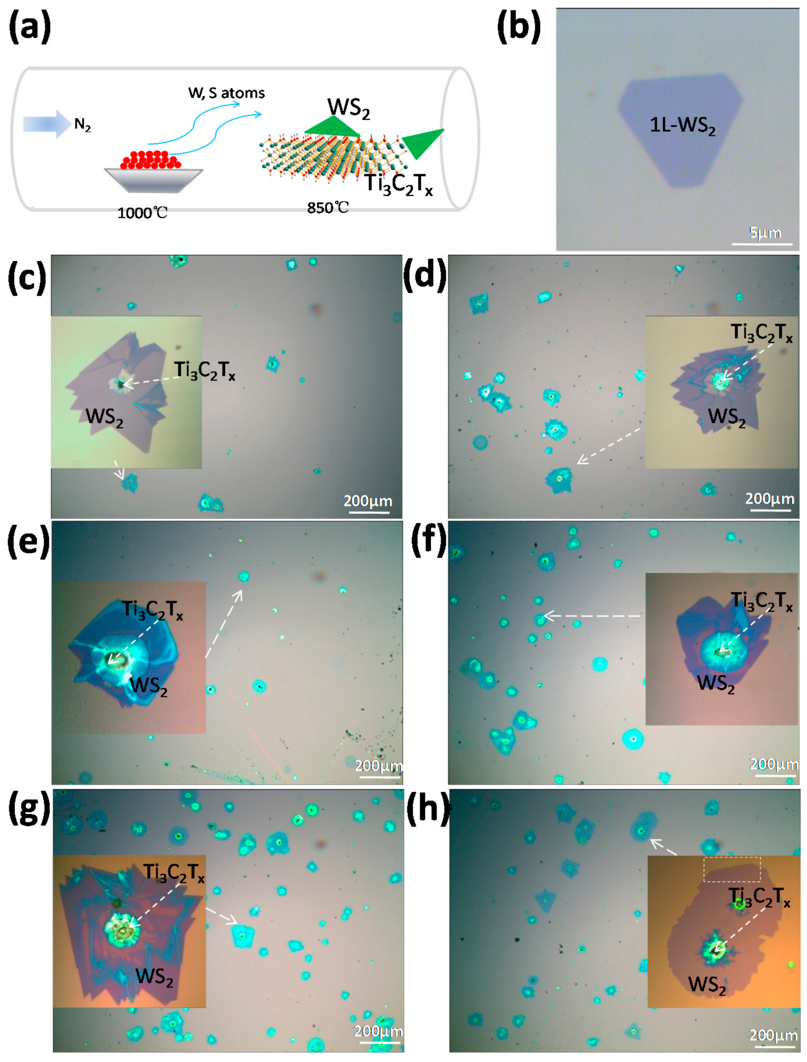
The VT routine was employed to deposit WS2 flakes. A schematic of deposition is shown in Figure 1a. For direct deposition of WS2 on Si/SiO2 (300 nm) substrates, the substrates were cleaned by deionized water, ethanol, and H2O2. For deposition of WS2 on mxene, Ti3C2Tx mxene prepared by standard procedure [16] (with a yield of ~72%) was ultrasonically exfoliated (700 W of ultrasonic power) for 1 h and spin coated on cleaned Si/SiO2 (300 nm) substrates. The typical size of ultrasonically exfoliated Ti3C2Tx mxene flakes on the substrate was 3–5 μm. The WS2 powders and substrates were loaded in a one-zone tube furnace with quartz tube diameter of 1 inch. The WS2 source was put at the center of the heating zone. The substrate was put at the down-steam low temperature area and the source-substrate distance was kept as 12 cm by moving the substrate. The source temperature was raised from room temperature to 1000 °C within 50 min, then held for 60 min, and finally cooled to ambient temperature naturally. Pure nitrogen gas with flow rate of 20 sccm was used as carrier gas.
2.2. Characterization
The optical images of WS2 and Ti3C2Tx mxene were obtained using an optical microscope. Micro Raman and PL measurements were conducted on a home built Raman/PL system, consisting of an inverted microscope (Ti eclipse, Nikon, Tokyo, Japan) and a Raman spectrometer (iHR320, Horiba, Palaiseau, France) attached with a CCD detector (Syncerity, Horiba, Palaiseau, France). A 532 nm laser was focused onto the sample using a 100×, 0.95 NA objective lens. The PL intensity images were recorded by a photoluminescence microscope with excitations of LED (light-emitting diode, central wavelength of 485 nm). The topographic images of samples were measured by an atomic force microscope (Innova, Bruker, Karlsruhe, Germany). Scanning electron microscopy (SEM) images were collected on a Hitachi JSM-6460 SEM (Hitachi, Tokyo, Japan).
Ti3C2Tx mxene has birefringence property [17]. The polarization direction of light reflected from mxene is altered to an angle differing to that of the incident light. However, this cannot occur with dust or WS2. Such an effect allows for the identification of Ti3C2Tx flakes from other objects (i.e., dusts) by using polarization optical microscope. At parallel configuration, i.e., where the polarization directions of two polarizers at incident and out-going light path of the microscope are parallel to each other, both Ti3C2Tx flakes and other objects without birefringence property can be seen (Figure S1a). However, at cross configuration, i.e., where the polarization directions of two polarizers are perpendicular to each other, the reflected light from objects without birefringence is blocked, while only Ti3C2Tx flakes are visible (Figure S1b). This simple method can also be used to distinguish WS2 flakes growing on Ti3C2Tx from those grown on SiO2 and dusts. The 1 L WS2 flakes growing around Ti3C2Tx flakes show light purple contrast at parallel configuration (Figure S1c), while becoming invisible at cross configuration (Figure S1d). However, the Ti3C2Tx flakes still show features similar to Figure S1b, i.e., bright contrast in cross configuration (Figure S1d).
3. Results and Discussion
3.1. Growth of WS2/Ti3C2Tx Mxene
An optical image of a truncated triangular WS2 flake deposited without Ti3C2Tx is shown in Figure 1b. Light purple contrast indicates that this is a 1 L flake, which can be confirmed by its single excitonic band with strong PL intensity (shown in the following sections). The growth of WS2 on Ti3C2Tx mxene strongly depends on the deposition pressure and the sample-source distance (D). The optical images of WS2 deposited with Ti3C2Tx mxene at pressures of 200 Torr and 250 Torr are shown in Figure 1c,d, respectively. At a low pressure of 200 Torr, the size of flake growing around mxene is quite small. Larger flakes with 1 L and few layers can be observed at high pressures as 250 Torr (Figure 1d) and 350 Torr (Figure 1e–h). The growth of WS2 flake also strongly depends on D. Figure 1e–h shows images of flakes with D of 9 cm, 9.5 cm, 10 cm, and 10.5 cm, respectively. At short D (9 cm) (Figure 1e), the WS2 tends to grow into thick flakes, while at long D (10.5–11 cm), 1 L WS2 flakes can be obtained (Figure 1g,h). It should be noted that at even larger D (D > 11 cm), WS2 islands instead of flakes are observed. An AFM topographic image of a 1 L WS2 flake area marked in Figure 1h is shown in Figure S2a. This 1 L WS2 flake is quite flat within the flake area. High density of nanocrystals can be observed at the WS2 flake edge and on the blank SiO2. These nanocrystals, which are usually found during vapor transportation growth [18], can be assigned to WS2. The thickness of 1 L WS2 can determined to be ~0.8 nm from the line profile across the edge (Figure S2b), which agrees well with the reported thickness of a 1 L WS2 flake [19].
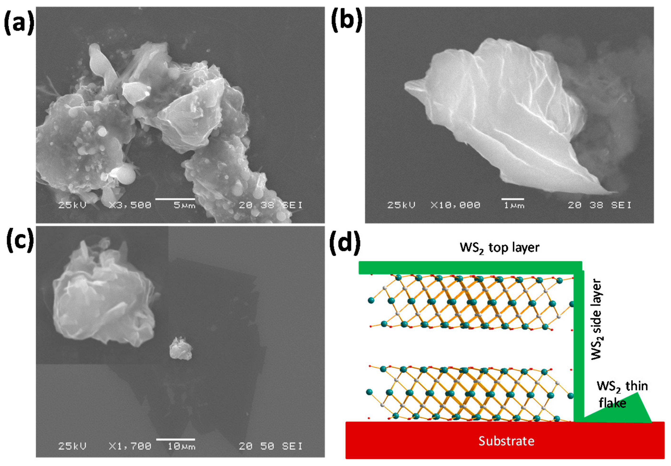
We also investigated the growth of WS2 flakes on the top of mxene flakes. Three typical SEM images are show in Figure 2a–c. Figure 2a shows a situation in which WS2 grows on a flat Ti3C2Tx flake sitting on the substrate. In this case WS2 grows on the top surface of this Ti3C2Tx flake and finally uniformly covers the top surface. This indicates WS2 can nucleate and grow on the surface of Ti3C2Tx flake easily. Figure 2b corresponds to WS2 grows on a Ti3C2Tx flake with terrace-like edges. In this image, the WS2 layer covers both the top surface and the lateral side of terrace-like edges. The disappearance of Ti3C2Tx edges in Figure 2a,b indicates the WS2 covers the whole lateral side. Figure 2c shows a feature slightly differing from Figure 2b: despite the WS2 coated on the lateral side of this Ti3C2Tx flake, many small petals also grow on the top and the lateral side. Based on Figure 2a–c, a possible growth model is proposed, and is schematically shown in Figure 2d. In this simple model, a bilayer Ti3C2Tx flake lies on the substrate. The Ti3C2Tx flake acts as an inhomogeneous nucleation agent, similar to the other precursors such as graphene and BN used in the growth of 1 L MoS2 and WS2 [20,21,22]. In inhomogeneous nucleation procedure, WS2 nucleates much more easily than the homogeneous nucleation owing to the reduced free energy [23]. The seeds of WS2 on the top surface and lateral side grow, and finally merge into a WS2 layer covering the whole surface of Ti3C2Tx mxene. The thickness of the top layer, which can be determined from their Raman and PL spectra (see following section for further discussions), also greatly depends on the growth conditions. Similar to other precursors again, the Ti3C2Tx flake is also a good inhomogeneous nucleation agent for growth of WS2 flakes on SiO2/Si substrate. Triangular flakes nucleating on some sites eat up the small islands surrounding the flake by diffusion and finally grow into a big WS2 flake. The final shape of this flake greatly depends on the number of nucleation sites. For few nucleation sites (such as Figure 1h), simple triangular flakes can be obtained, while for a Ti3C2Tx flake with large number of nucleation sites, a polygon shape flake with a number of corners can be obtained (Figure 1g).
3.2. Optical Characterization of WS2/Ti3C2Tx Mxene
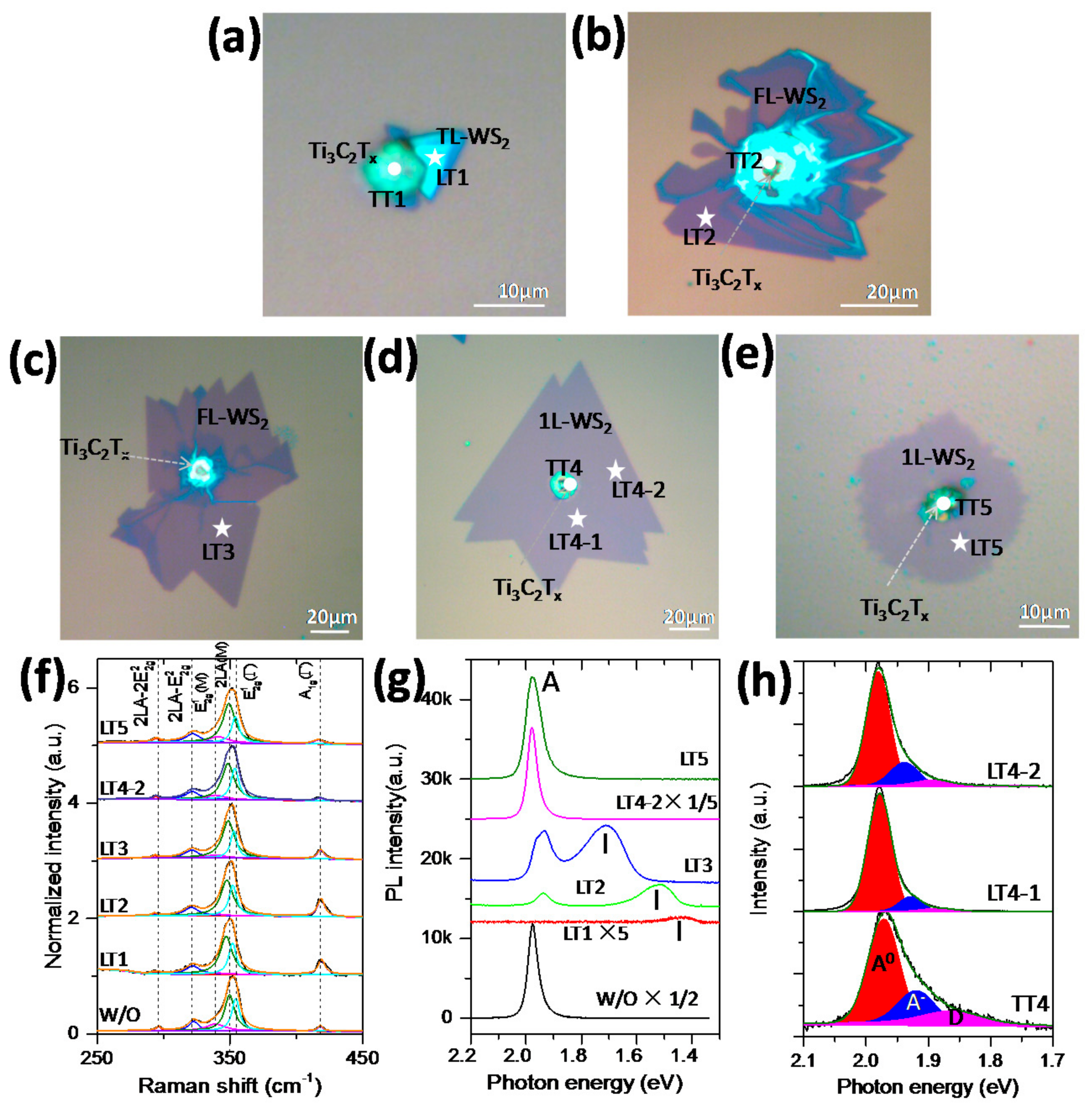
In order to investigate the optical properties of WS2 growing on Ti3C2Tx mxene, five WS2 flakes named by T1–T5 are selected from Figure 1e–h, and their optical images are shown in Figure 3a–e, respectively. From T1 to T5, the optical contrast changes from high contrast (T1, Figure 3a) to deep purple (T2 in Figure 3b and T3 in Figure 3c), and finally light purple (T4 in Figure 3d and T5 in Figure 3e), which indicates T1 is a thick-layer (TL) flake, T2 and T3 are few layer (FL) flakes, while T4 and T5 are 1 L flakes. Raman spectra collected from locations LT1–LT5 marked on flakes T1–T5 are shown in Figure 3f. A Raman spectrum of 1 L WS2 in Figure 1b is also shown for comparison. At a laser excitation wavelength of 532 nm, the Raman spectra of WS2 flakes exhibit features of first-order and second-order blended Raman modes, which are similar to previous reports [19,24]. The Raman peak at 417.8 cm−1 can be assigned to A1g (out-of-plane mode). The peak at 351.3 cm−1 can be assigned to the blended modes of (in-plane mode) and 2LA mode (M point of first Brillion zone). The Raman peaks at 324.1 and 296.2 cm−1 can be assigned to second order Raman modes of and , respectively [19,24]. As the most distinguishable feature, the intensity of A1g peak subsequently decreases from LT1 to LT5. This agrees well with previous reports, and can be attributed to the decreasing layer thickness [25,26]. The shift of A1g peak can also be used to determine the layer thickness [25,26]. The A1g Raman peaks of flakes T1–T5 collected at LT1–LT5 are plotted in Figure S3a. A red shift of A1g peak can be observed with decreasing layer thickness. We further fitted the A1g peak by using a Lorentzian function. The obtained peak positions are shown in Figure S3b. For thick layer flake T1, the peak position of A1g is 419.2 cm−1, corresponding to the peak position of thick layer [25,26].
For flakes T2 and T3, the A1g peak shifts to 418.5 and 418 cm−1, indicating trilayer and bilayer of these two flakes [25,26], respectively. The average peak position of T4, T5, and 1 L flake deposition without mxene is 416.9 cm−1, confirming the 1 L characteristic of these three flakes [25,26].
PL spectra of WS2 flakes growing surrounding the central Ti3C2Tx flake of samples were also collected from locations LT1–LT5, and are shown in Figure 3g. For comparison, the PL spectrum of 1 L WS2 flake in Figure 1b is also shown in Figure 3g. According to the previous reports [3,27], excitons generated by the direct band transition in 1 L WS2 show a single PL peak, while double wavelet PL bands originating from excitonic transitions belonging to the direct band transition (K-K) and indirect band transition are always observed on few layer (layer numbers 2–4) WS2 flakes. In the PL spectrum of 1 L flake in Figure 1b, the strong single PL peak centered at 1.98 eV can be assigned to A exciton band of 1 L WS2. Flake T1 shows a broad PL peak centered at 1.44 eV (marked as I), which fits the indirect excitonic transition energy of thick layer with layer numbers >4 layer [28]. The PL spectrum of T2 exhibits a broad peak at 1.52 eV and a sharp peak at 1.94 eV, which corresponds to the excitonic transition of indirect (I) and direct band (A), respectively [29]. The energy of indirect band transition agrees well with the indirect band transition energy of trilayer WS2 flake [29]. Similar to T2, T3 shows two PL peaks at 1.94 eV and 1.72 eV, which correspond to the direct and the indirect excitonic transition bands, respectively, of bilayer very well [29]. Single excitoic peak feature of T4 and T5 at 1.98 eV agrees well with that of WS2 deposited without mxene and the reported excitonic energy of 1 L WS2, confirming the 1 L nature of T4 and T5 [29,30]. It should be noted that the PL intensity of T5 is only 20% of T4. Meanwhile, its peak width of 68 meV is also larger than that of T4 (47 meV), which possibly be induced by high density of defects in T5 [31].
PL spectra are also measured on the top of Ti3C2Tx flakes coated with WS2 (locations TT1, TT2, TT4, and TT5 marked in Figure 3a,b,d,e), shown in Figure S4. Owing to the growth of WS2 on the top surface, these Ti3C2Tx flake exhibit PL characteristics of WS2 flakes. PL spectra collected from locations TT1 and TT2 show double PL bands, which indicates the WS2 growing on the top surfaces of mxenes in T1 and T2 are thick layers (Figure S4a). Single PL peaks with energies at 1.96 eV and 1.95 eV of locations TT4 and TT5 indicate the WS2 flakes growing on the top surface of mxenes in T4 and T5 are 1 L (Figure S4b). In Figure S4b, the WS2 flake on the top of a Ti3C2Tx flake shows a PL peak much broader (FWHM = 83 meV) than that of 1 L WS2 flake growing around this Ti3C2Tx flake (FWHM = 47 meV). The PL intensity of TT4 is greatly quenched by ~50 times in contrast to that of LT4-1. On the PL spectra of TT4 and TT5, a long PL tail is observed at the low energy side. A further deconvolution of PL spectra collected at locations TT4 and LT4-1 of 1 L WS2 flake T4 was performed using three Gaussian functions, and is shown in Figure 3h. These three functions represent the neutral exciton (A0) at ~1.97 eV, trion (A−) at ~1.92 eV and exciton trapped on defects (D) at ~1.86 eV, respectively. In contrast to PL energy of LT4-1, the A0 exciton energy of TT4 redshifts by ~19 meV. Meanwhile, the normalized PL intensity of A− and D excitons of TT4 are also enhanced. Auger recombination at WS2/Ti3C2Tx interface is the first possible reason quenching the PL intensity of TT4. The PL intensity of MoS2 can be greatly quenched at MoS2/graphene [32] and MoS2/Au [33] contact due to strong Auger recombination. The electric conductivity of Ti3C2Tx is 4.2 × 10⁻⁴ S/m [9], which is comparable to graphene. Similar to the PL quenching observed at graphene/TMD interface, the Auger recombination at WS2/Ti3C2Tx interface can also greatly reduce the PL intensity of WS2 [32]. However, simple Ohmic contact of WS2 to conductor would not cause strongly enhanced D exciton signal [34,35]. Therefore, defects related nonradiative recombination should be considered as the second possible reason inducing PL quenching [36]. According to a study by Kim et al. [30], strong intensity of this PL tail indicates a high density of excitons trapped on defects. High intensity of D exciton peak indicates high density of defects of 1 L WS2 growing on mxene [37]. We suspect that this high density of defects reduces the PL intensity of A0 and A− excitons via the non-recombination process [36]. In our previous study, we found the increasing density of Se adtoms can effectively reduce the band gap of 1 L WSe2 [38], inducing the redshift of excitonic energy. We suspect that observed red shift of A0 exciton of 1 L WS2 growing on Ti3C2Tx mxene is induced by the same factor. The dielectric constant of Ti3C2Tx (εr = 2.5 and εi = 3.5) [39] is slightly larger than that of SiO2 (εr = 2.1 and εi = 0) [40]. According to the study of Lin et al., increasing environmental dielectric constant causes blue shift of excitonic energy [41], which is contrary to red shift of the excitonic energy of WS2 deposited on Ti3C2Tx as comparison to that of WS2 deposited on SiO2. Therefore, the dielectric screening effect can be ruled out.
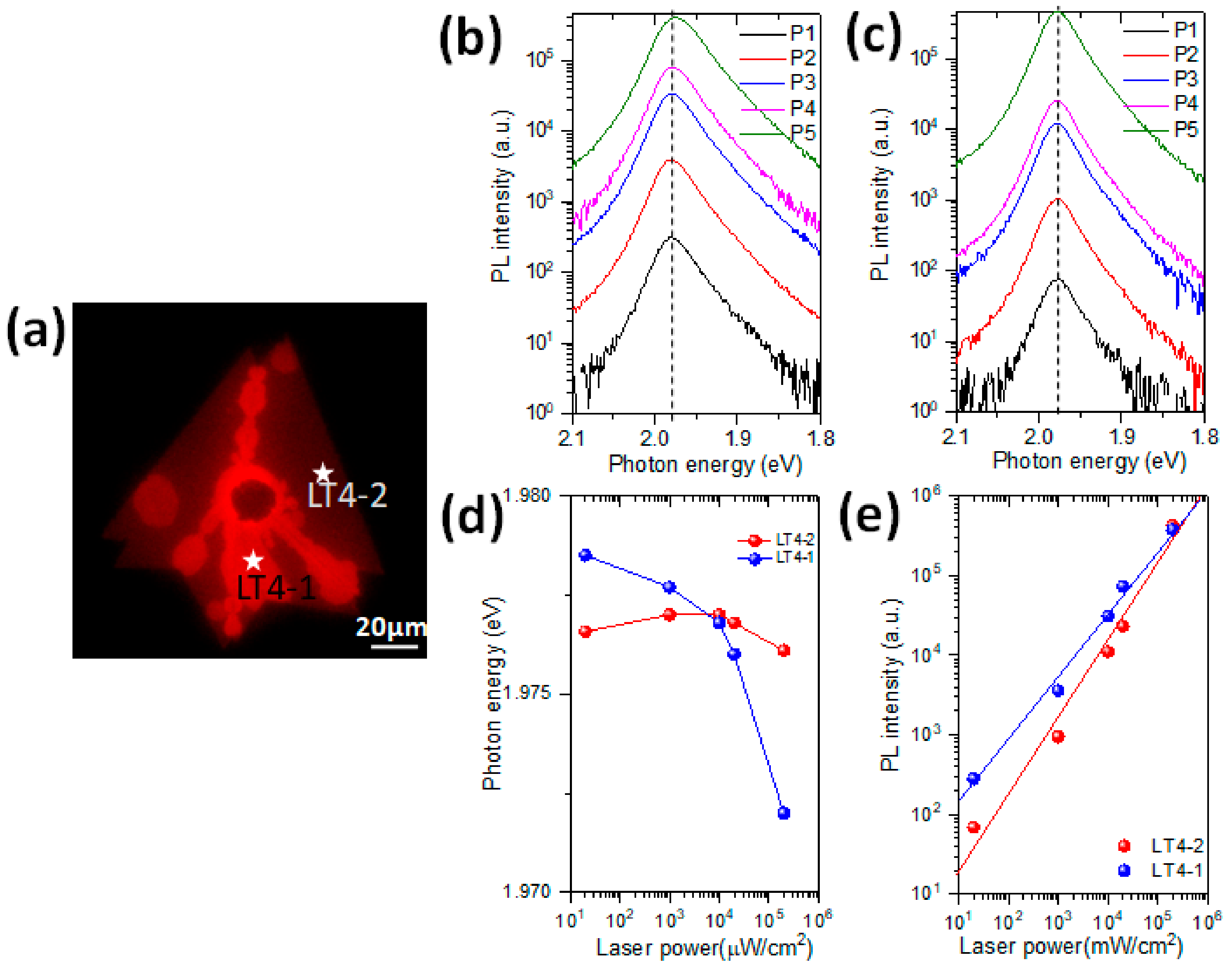
A PL image of the 1 L WS2 flake in Figure 3d is shown in Figure 4a. Although the shape of this flake measured by PL imaging fits that measured by optical image (Figure 3d), the PL intensity varies greatly at different positions. The PL intensity is strong at the grain boundary and the interface between WS2 and Ti3C2Tx, but weak at other points. Normalized PL spectra of LT4-2 as comparison to LT4-1 are shown in Figure 3h. It can be seen the PL spectrum of LT4-1 is broader than LT4-2. Simultaneously, a blue shift of LT4-1 is observed in contrast to LT4-2. We further fit these two PL spectra using three Gaussian peaks, representing three exciton states of A0, A− and D (shown in Figure 3h), respectively. It can be seen the D exciton band of LT4-1 is stronger than that of LT4-2. In previous reports of Kim et al. [30], Gutierrez et al. [3] and Peimyoo et al. [19], different authors observed PL enhancement at edges and grain boundaries of CVD (chemical vapor deposition) deposited 1 L WS2 flakes. They attributed this PL enhancement to the high density of sulphur vacancies at the edges and grain boundaries [3,19,30]. In our study, PL enhancement is observed inside 1 L flake, but absent at its edges (Figure 4a and Figure S5). It should be mentioned that the 1 L flakes shown in Figure 4a and Figure S5 are polycrystalline instead of single crystal. The areas with enhanced PL intensity are almost along the grain boundary. We suspect this is caused by a different distribution of sulphur defects. The presence of Ti3C2Tx mxene induces high density of sulphur vacancies only at grain boundary, but not on the edges, which finally induces the high PL intensity at grain boundaries observed in Figure 4a. Moreover, the PL energy of LT4-1 slightly blue shifted by 3 meV compared to that of LT4-2. Such blueshift is similar to that on defect area of 1 L WS2 observed by Kim et al. [30]. This indicates that the defects on our sample are also similar to the sulphur vacancies existing on samples of Kim et al. [30].
The laser power dependent PL of position LT4-1 and LT4-2 were measured at five different laser powers (0.02 μW, 1 μW, 10 μW, 20 μW, and 200 μW). Their obtained PL spectra are plotted in Figure 4b,c, respectively. At low excitation power (<20 μW), the PL intensity of LT4-1 is higher than that of LT4-2. At high excitation power, the measured PL intensity of LT4-2 becomes slightly stronger than LT4-1. The PL peak position as a function of excitation laser power density is plotted in Figure 4d. At low excitation power density, the PL energy of LT4-1 is higher than LT4-2. With increasing excitation laser power density, the peak energy of LT4-2 hardly shifts, while LT4-1 decreases faster. When the excitation laser power is higher than 10 μW, the PL peak energy of LT4-1 becomes lower than LT4-2. This laser power dependent PL peak shift is very similar to that reported by Kim et al. [30]. In their study, the peak energy versus laser power curves of inner part of 1 L WS2 also intercepts with that of edge at ~10 μW [30]. It should be noted that the edges of WS2 samples used by Kim et al. have a higher density of defects than the inner parts [30]. Peak position versus laser power trend in our study is similar to that of Kim et al., indicating the role of defect at LT4-1 causing such PL energy shift.
As shown in Figure 3h, the intensities of A− and D excitons are much lower than those of A0 exciton. Deconvolution of PL spectra measured at low laser power by using these three excitons always gives large uncertainty. Clear trends of PL intensity of different excitons versus excitation laser power are difficult to be obtained. However, the PL intensity of the whole A band versus laser power is straightforward and can be used for analysis. The PL intensity of A band measured at different laser power is clearly shown by a logarithmic plot (Figure 4f). We further fitted these data using the dependence I = Pm, where I, P and m are PL intensity, laser power density, and numeric power [30,42]. The obtained m for LT4-1 and LT4-2 are 0.8 and 0.94, respectively. This sublinear dependence had been observed by different authors [30,43], indicating the role of defect. With a higher density of defects, more excitons generated at increasing laser power are trapped by defects, inducing low PL intensity increasing with laser power and a smaller m [43].
4. Conclusions
In summary, we deposited WS2 thin flakes on Ti3C2Tx mxene using vapor transportation method. Ti3C2Tx mxene acts as good nucleation seed for WS2. WS2 can easily nucleate and grow on the top surface and lateral edges of Ti3C2Tx mxene. By optimizing growth conditions, multilayer, few layer, and 1 L WS2 flakes can be deposited. A high density of defect is observed on 1 L WS2 flakes growing on the top surface of Ti3C2Tx, which greatly reduced their PL intensity. Our study would benefit the preparation of future 1 L WS2/Ti3C2Tx junctions and their further potential applications in electronics devices.
Supplementary Materials
The following are available online at https://www.mdpi.com/2079-6412/8/8/281/s1, Figure S1: Optical image of a mxene flake at parallel (a) and cross (b) polarization; Optical image of a mxene coated with monolayer WS2 measured at parallel (c) and cross (d) polarization; Figure S2: (a) AFM image of a corner of a monolayer WS2 flake marked in Figure 1h; (b) the height profile of this flake along the dashed line in (a); Figure S3: (a) A1g Raman peaks of different WS2 flakes; (b) The fitted A1g peak positions of different WS2 flakes. W/O denotes the monolayer WS2 flake deposited without mxene; Figure S4: (a) PL spectra collected from locations TT1 and TT2(marked in Figure 3a,b) the top of mxene in T1 and T2; (b) PL spectra collected from locations TT4 and TT5 (marked in Figure 3d,e) the top of mxene in T4 and T5; Figure S5: (a,c) Optical images of two monolayer WS2 flakes and their corresponding PL images (b,d), respectively.
Author Contributions
Conceptualization, W.S.; Methodology, W.S.; Writing—Original Draft Preparation, W.S.; Investigation, S.W., L.F., and F.C.; Formal analysis, K.S., L.Y., and X.H.
Funding
This research was funded by Zhejiang Provincial Natural Science Foundation of China (LY18F040006) and Natural Sciences Foundation of China (No. 61306115, 61775201, and 11404309).
Acknowledgments
The authors acknowledged Shichao Zhao (Hangzhou Dianzi University) for fruitful discussion of data processing.
Conflicts of Interest
The authors declare no conflict of interest.
References
- Chernikov, A.; Berkelbach, T.C.; Hill, H.M.; Rigosi, A.; Li, Y.; Aslan, O.B.; Reichman, D.R.; Hybertsen, M.S.; Heinz, T.F. Exciton binding energy and nonhydrogenic rydberg series in monolayer WS2. Phys. Rev. Lett. 2014, 113, 076802. [Google Scholar] [CrossRef] [PubMed]
- Yuan, L.; Huang, L. Exciton dynamics and annihilation in WS2 2D semiconductors. Nanoscale 2015, 7, 7402–7408. [Google Scholar] [CrossRef] [PubMed]
- Gutierrez, H.R.; Perea-Lopez, N.; Elias, A.L.; Berkdemir, A.; Wang, B.; Lv, R.; Lopez-Urias, F.; Crespi, V.H.; Terrones, H.; Terrones, M. Extraordinary room-temperature photoluminescence in triangular WS2 monolayers. Nano Lett. 2013, 13, 3447–3454. [Google Scholar] [CrossRef] [PubMed]
- Mouri, S.; Miyauchi, Y.; Toh, M.; Zhao, W.; Eda, G.; Matsuda, K. Nonlinear photoluminescence in atomically thin layered WSe2 arising from diffusion-assisted exciton-exciton annihilation. Phys. Rev. B 2014, 90, 155499. [Google Scholar] [CrossRef]
- Sundaram, R.S.; Engel, M.; Lombardo, A.; Krupke, R.; Ferrari, A.C.; Avouris, P.; Steiner, M. Electroluminescence in single layer MoS2. Nano Lett. 2013, 13, 1416–1421. [Google Scholar] [CrossRef] [PubMed]
- He, Y.M.; Clark, G.; Schaibley, J.R.; He, Y.; Chen, M.C.; Wei, Y.J.; Ding, X.; Zhang, Q.; Yao, W.; Xu, X.; et al. Single quantum emitters in monolayer semiconductors. Nat. Nanotechnol. 2015, 10, 497–502. [Google Scholar] [CrossRef] [PubMed] [Green Version]
- Naguib, M.; Come, J.; Dyatkin, B.; Presser, V.; Taberna, P.L.; Simon, P.; Barsoum, M.W.; Gogotsi, Y. Mxene: A promising transition metal carbide anode for lithium-ion batteries. Electrochem. Commun. 2012, 16, 61–64. [Google Scholar] [CrossRef]
- Come, J.; Naguib, M.; Rozier, P.; Barsoum, M.W.; Gogotsi, Y.; Taberna, P.L.; Morcrette, M.; Simon, P. A non-aqueous asymmetric cell with a Ti2C-based two-dimensional negative electrode. J. Electrochem. Soc. 2012, 159, A1368–A1373. [Google Scholar] [CrossRef]
- Han, M.; Yin, X.; Wu, H.; Hou, Z.; Song, C.; Li, X.; Zhang, L.; Cheng, L. Ti3C2 mxenes with modified surface for high-performance electromagnetic absorption and shielding in the x-band. ACS Appl. Mater. Interfaces 2016, 8, 21011–21019. [Google Scholar] [CrossRef] [PubMed]
- Tang, Q.; Zhou, Z.; Shen, P. Are mxenes promising anode materials for li ion batteries? Computational studies on electronic properties and Li storage capability of Ti3C2 and Ti3C2X2 (X = F, OH) monolayer. J. Am. Chem. Soc. 2012, 134, 16909–16916. [Google Scholar] [CrossRef] [PubMed]
- Naguib, M.; Mashtalir, O.; Carle, J.; Presser, V.; Lu, J.; Hultman, L.; Gogotsi, Y.; Barsoum, M.W. Two-dimensional transition metal carbides. ACS Nano 2012, 6, 1322–1331. [Google Scholar] [CrossRef] [PubMed]
- Li, X.; Dai, Y.; Ma, Y.; Liu, Q.; Huang, B. Intriguing electronic properties of two-dimensional MoS2/TM2CO2 (TM = Ti, Zr, or Hf) hetero-bilayers: Type-II semiconductors with tunable band gaps. Nanotechnology 2015, 26, 135703. [Google Scholar] [CrossRef] [PubMed]
- Ma, Z.; Hu, Z.; Zhao, X.; Tang, Q.; Wu, D.; Zhou, Z.; Zhang, L. Tunable band structures of heterostructured bilayers with transition-metal dichalcogenide and mxene monolayer. J. Phys. Chem. C 2014, 118, 5593–5599. [Google Scholar] [CrossRef]
- Wu, Y.; Nie, P.; Jiang, J.; Ding, B.; Dou, H.; Zhang, X. MoS2-nanosheet-decorated 2D titanium carbide (mxene) as high-performance anodes for sodium-ion batteries. Chemelectrochem 2017, 4, 1560–1565. [Google Scholar] [CrossRef]
- Xu, J.; Shim, J.; Park, J.H.; Lee, S. Mxene electrode for the integration of WSe2 and MoS2 field effect transistors. Adv. Funct. Mater. 2016, 26, 5328–5334. [Google Scholar] [CrossRef]
- Naguib, M.; Kurtoglu, M.; Presser, V.; Lu, J.; Niu, J.; Heon, M.; Hultman, L.; Gogotsi, Y.; Barsoum, M.W. Two-dimensional nanocrystals produced by exfoliation of Ti3AlC2. Adv. Mater. 2011, 23, 4248–4253. [Google Scholar] [CrossRef] [PubMed]
- Seyedin, S.; Yanza, E.R.S.; Razal, J.M. Knittable energy storing fiber with high volumetric performance made from predominantly mxene nanosheets. J. Mater. Chem. A 2017, 5, 24076–24082. [Google Scholar] [CrossRef]
- Su, W.; Li, Y.; Jin, L.; Chen, L.; Song, K.; Huang, X.; Hong, X. Deposition of porous few-layer WSe2 flakes with high density of exposed edge sites. Vacuum 2017, 145, 4–10. [Google Scholar] [CrossRef]
- Peimyoo, N.; Shang, J.; Cong, C.; Shen, X.; Wu, X.; Yeow, E.K.L.; Yu, T. Nonblinking, intense two-dimensional light emitter: Mono layer WS2 triangles. ACS Nano 2013, 7, 10985–10994. [Google Scholar] [CrossRef] [PubMed]
- Okada, M.; Sawazaki, T.; Watanabe, K.; Taniguch, T.; Hibino, H.; Shinohara, H.; Kitaura, R. Direct chemical vapor deposition growth of WS2 atomic layers on hexagonal boron nitride. ACS Nano 2014, 8, 8273–8277. [Google Scholar] [CrossRef] [PubMed]
- Ling, X.; Lee, Y.H.; Lin, Y.; Fang, W.; Yu, L.; Dresselhaus, M.S.; Kong, J. Role of the seeding promoter in MoS2 growth by chemical vapor deposition. Nano Lett. 2014, 14, 464–472. [Google Scholar] [CrossRef] [PubMed]
- Shi, Y.; Zhou, W.; Lu, A.Y.; Fang, W.; Lee, Y.H.; Hsu, A.L.; Kim, S.M.; Kim, K.K.; Yang, H.Y.; Li, L.J.; et al. Van der waals epitaxy of MoS2 layers using graphene as growth templates. Nano Lett. 2012, 12, 2784–2791. [Google Scholar] [CrossRef] [PubMed]
- Zhang, D.; Wu, R. Fundamentals of Materials Science; Peking University Press: Beijing, China, 2011; Volume 1. (In Chinese) [Google Scholar]
- He, Z.; Wang, X.; Xu, W.; Zhou, Y.; Sheng, Y.; Rong, Y.; Smith, J.M.; Warner, J.H. Revealing defect-state photoluminescence in monolayer WS2 by cryogenic laser processing. ACS Nano 2016, 10, 5847–5855. [Google Scholar] [CrossRef] [PubMed]
- Berkdemir, A.; Gutierrez, H.R.; Botello-Mendez, A.R.; Perea-Lopez, N.; Elias, A.L.; Chia, C.I.; Wang, B.; Crespi, V.H.; Lopez-Urias, F.; Charlier, J.C.; et al. Identification of individual and few layers of WS2 using Raman spectroscopy. Sci. Rep. 2013, 3, 1755. [Google Scholar] [CrossRef]
- Staiger, M.; Gillen, R.; Scheuschner, N.; Ochedowski, O.; Kampmann, F.; Schleberger, M.; Thomsen, C.; Maultzsch, J. Splitting of monolayer out-of-plane A1’ Raman mode in few-layer WS2. Phys. Rev. B 2015, 91, 195419. [Google Scholar] [CrossRef]
- Zhang, Y.; Zhang, Y.; Ji, Q.; Ju, J.; Yuan, H.; Shi, J.; Gao, T.; Ma, D.; Liu, M.; Chen, Y.; et al. Controlled growth of high-quality monolayer WS2 layers on sapphire and imaging its grain boundary. ACS Nano 2013, 7, 8963–8971. [Google Scholar] [CrossRef] [PubMed]
- Zeng, H.; Liu, G.B.; Dai, J.; Yan, Y.; Zhu, B.; He, R.; Xie, L.; Xu, S.; Chen, X.; Yao, W.; et al. Optical signature of symmetry variations and spin-valley coupling in atomically thin tungsten dichalcogenides. Sci. Rep. 2013, 3, 1608. [Google Scholar] [CrossRef] [PubMed] [Green Version]
- Zhao, W.; Ghorannevis, Z.; Chu, L.; Toh, M.; Kloc, C.; Tan, P.H.; Eda, G. Evolution of electronic structure in atomically thin sheets of WS2 and WSe2. ACS Nano 2013, 7, 791–797. [Google Scholar] [CrossRef] [PubMed]
- Kim, M.S.; Yun, S.J.; Lee, Y.; Seo, C.; Han, G.H.; Kim, K.K.; Lee, Y.H.; Kim, J. Biexciton emission from edges and grain boundaries of triangular WS2 monolayers. ACS Nano 2016, 10, 2399–2405. [Google Scholar] [CrossRef] [PubMed]
- McCreary, A.; Berkdemir, A.; Wang, J.; Minh An, N.; Elias, A.L.; Perea-Lopez, N.; Fujisawa, K.; Kabius, B.; Carozo, V.; Cullen, D.A.; et al. Distinct photoluminescence and Raman spectroscopy signatures for identifying highly crystalline WS2 monolayers produced by different growth methods. J. Mater. Res. 2016, 31, 931–944. [Google Scholar] [CrossRef]
- Shih, C.J.; Wang, Q.H.; Son, Y.; Jin, Z.; Blankschtein, D.; Strano, M.S. Tuning on-off current ratio and field-effect mobility in a MoS2-graphene heterostructure via Schottky barrier modulation. ACS Nano 2014, 8, 5790–5798. [Google Scholar] [CrossRef] [PubMed]
- Bhanu, U.; Islam, M.R.; Tetard, L.; Khondaker, S.I. Photoluminescence quenching in gold-MoS2 hybrid nanoflakes. Sci. Rep. 2014, 4, 5575. [Google Scholar] [CrossRef] [PubMed]
- Su, W.; Kumar, N.; Mignuzzi, S.; Crain, J.; Roy, D. Nanoscale mapping of excitonic processes in single-layer MoS2 using tip-enhanced photoluminescence microscopy. Nanoscale 2016, 8, 10564–10569. [Google Scholar] [CrossRef] [PubMed]
- Kim, J.Y.; Kim, J.; Joo, J. Surface-enhanced Raman scattering for 2-D WSe2 hybridized with functionalized gold nanoparticles. Opt. Express 2016, 24, 27546–27553. [Google Scholar] [CrossRef] [PubMed]
- Su, W.; Jin, L.; Qu, X.; Huo, D.; Yang, L. Defect passivation induced strong photoluminescence enhancement of rhombic monolayer MoS2. Phys. Chem. Chem. Phys. 2016, 18, 14001–14006. [Google Scholar] [CrossRef] [PubMed]
- Chow, P.K.; Jacobs-Gedrim, R.B.; Gao, J.; Lu, T.M.; Yu, B.; Terrones, H.; Koratkar, N. Defect-induced photoluminescence in mono layer semiconducting transition metal dichalcogenides. ACS Nano 2015, 9, 1520–1527. [Google Scholar] [CrossRef] [PubMed]
- Su, W.; Li, Y.; Chen, L.; Huo, D.; Song, K.; Huang, X.; Shu, H. Nonstoichiometry induced broadband tunable photoluminescence of monolayer WSe2. Chem. Commun. 2018, 54, 743–746. [Google Scholar] [CrossRef] [PubMed]
- Berdiyorov, G.R. Optical properties of functionalized Ti3C2T2 (T = F, O, OH) mxene: First-principles calculations. AIP Adv. 2016, 6, 055105. [Google Scholar] [CrossRef]
- Palik, E.D. Handbook of Optical Constants of Solids, 1st ed.; Academic Press: London, UK, 1998. [Google Scholar]
- Lin, Y.; Ling, X.; Yu, L.; Huang, S.; Hsu, A.L.; Lee, Y.H.; Kong, J.; Dressehaus, M.S.; Palacios, T. Dielectric screening of excitons and trions in single-layer MoS2. Nano Lett. 2014, 14, 5569–5576. [Google Scholar] [CrossRef] [PubMed]
- Suh, J.; Tan, T.L.; Zhao, W.; Park, J.; Lin, D.Y.; Park, T.E.; Kim, J.; Jin, C.; Saigal, N.; Ghosh, S.; et al. Reconfiguring crystal and electronic structures of MoS2 by substitutional doping. Nat. Commun. 2018, 9, 199. [Google Scholar] [CrossRef] [PubMed]
- Carozo, V.; Wang, Y.; Fujisawa, K.; Carvalho, B.R.; McCreary, A.; Feng, S.; Lin, Z.; Zhou, C.; Perea-Lopez, N.; Laura Elias, A.; et al. Optical identification of sulfur vacancies: Bound excitons at the edges of monolayer tungsten disulfide. Sci. Adv. 2017, 3, e1602813. [Google Scholar] [CrossRef] [PubMed]
Figure 1.
(a) Schematic of vapor transportation setup used in this study; (b) optical image of a WS2 1 L flake deposited without Ti3C2Tx mxene; Optical image of WS2 flakes deposited at (c) 200 Torr and (d) 250 Torr. Optical images of WS2 growing at 350 Torr and different substrate-source distance (e) 10 cm, (f) 10.5 cm, (g) 11 cm and (h) 11.5 cm. The insets give magnified images of the marked flakes.

Figure 2.
Morphology of WS2 flakes growing on different Ti3C2Tx flakes (a–c); (d) Schematic of possible growth mechanism of WS2 on Ti3C2Tx flakes. The inset of Figure 2c shows the magnified SEM image of WS2 petals on Ti3C2Tx. Note the flakes in (a–c) are chosen from samples deposited at 350 Torr.
Figure 2.
Morphology of WS2 flakes growing on different Ti3C2Tx flakes (a–c); (d) Schematic of possible growth mechanism of WS2 on Ti3C2Tx flakes. The inset of Figure 2c shows the magnified SEM image of WS2 petals on Ti3C2Tx. Note the flakes in (a–c) are chosen from samples deposited at 350 Torr.

Figure 3.
(a–e): optical images of five WS2 flakes (T1–T5) with different thickness deposited with Ti3C2Tx mxene; (f) Raman and (g) PL spectra of collected on locations LT1–LT5 on WS2 flake T1–T5; (h) Deconvolution of PL spectra collected from different locations TT4, LT4-1 and LT4-2 (marked in (d)) of WS2 flake T4. Note that the PL intensities of some flakes are divided by a factor for clear comparison. The Raman spectra are normalized for clear comparison. The Raman and PL spectra of 1 L-WS2 deposited without mxene (W/O) in Figure 1b are also shown in (f,g), respectively, for comparison.

Figure 4.
(a) Photoluminescence microscopy image of a WS2 1 L flake (flake T4 in Figure 3d), measured with LED irradiation, corresponding to low power); (b,c), PL spectra of points LT4-1 and LT4-2 with different laser power, respectively; (d) PL A band positions of points LT4-1 and LT4-2 at different excitation laser power density; (e) PL A band intensities of points LT4-1 and LT4-2 as a function of different laser power densities (symbols), fitting using a function of I = Pm (solid line). Note that in (b,c), the PL intensities are plotted in logarithmic scale to clearly show the PL intensity change. The laser powers are P1 = 0.02 μW, P2 = 1 μW, P3 = 10 μW, P4 = 20 μW and P5 = 200 μW.
© 2018 by the authors. Licensee MDPI, Basel, Switzerland. This article is an open access article distributed under the terms and conditions of the Creative Commons Attribution (CC BY) license (http://creativecommons.org/licenses/by/4.0/).
Share and Cite
MDPI and ACS Style
Su, W.; Wang, S.; Fu, L.; Chen, F.; Song, K.; Huang, X.; Yang, L. Growth of WS2 flakes on Ti3C2Tx Mxene Using Vapor Transportation Routine. Coatings 2018, 8, 281. https://doi.org/10.3390/coatings8080281
AMA Style
Su W, Wang S, Fu L, Chen F, Song K, Huang X, Yang L. Growth of WS2 flakes on Ti3C2Tx Mxene Using Vapor Transportation Routine. Coatings. 2018; 8(8):281. https://doi.org/10.3390/coatings8080281
Chicago/Turabian StyleSu, Weitao, Shenguang Wang, Li Fu, Fei Chen, Kaixin Song, Xiwei Huang, and Li Yang. 2018. "Growth of WS2 flakes on Ti3C2Tx Mxene Using Vapor Transportation Routine" Coatings 8, no. 8: 281. https://doi.org/10.3390/coatings8080281
Note that from the first issue of 2016, this journal uses article numbers instead of page numbers. See further details here.