Electrochemical Performance of Few-Layer Graphene Nano-Flake Supercapacitors Prepared by the Vacuum Kinetic Spray Method


School of Mechanical Engineering, University of Ulsan, Ulsan 44610, Korea
*
Author to whom correspondence should be addressed.
Coatings 2018, 8(9), 302; https://doi.org/10.3390/coatings8090302
Submission received: 1 July 2018
/
Revised: 16 August 2018
/
Accepted: 24 August 2018
/
Published: 27 August 2018
(This article belongs to the Special Issue Thin Films for Energy Harvesting, Conversion, and Storage)
Abstract
:A few-layer graphene nano-flake thin film was prepared by an affordable vacuum kinetic spray method at room temperature and modest low vacuum conditions. In this economical approach, graphite microparticles, a few layers thick, are deposited on a stainless-steel substrate to form few-layer graphene nano-flakes using a nanoparticle deposition system (NPDS). The NPDS allows for a large area deposition at a low cost and can deposit various metal oxides at room temperature and low vacuum conditions. The morphology and structure of the deposited thin films are alterable by changing the scan speed of the deposition. These changes were verified by field emission scanning electron microscopy (FE-SEM), transmission electron microscopy (TEM), X-ray diffraction (XRD), and Raman spectroscopy. The electrochemical performances of the supercapacitors, fabricated using the deposited films and H3PO4–PVA gel electrolytes with different concentrations, were measured using a 2-electrode cell. The electrochemical performance was evaluated by cyclic voltammetry, galvanostatic Charge–discharge, and electrochemical impedance spectroscopy. The proposed affordable fabricated supercapacitors show a high areal capacitance and a small equivalent series resistance.
1. Introduction
Supercapacitors, also called ultracapacitors, are promising electrochemical storage devices due to their high-power density, fast charge/discharge rates, and long Charge–discharge cycles [1,2,3,4]. Supercapacitors have the potential to supplement or replace the use of batteries for energy storage applications, namely those for wearable and portable electronics, energy storage systems, and electrical and hybrid vehicles [5]. There are two representative types of supercapacitor: (1) the electric double layer capacitor (EDLC); and (2) the pseudocapacitor. EDLCs store energy via ion adsorption/desorption on the electrode surface, exhibit an excellent cycle life and power density, but are restrained by limited adsorption capacity, which adversely impacts their energy density [6]. Carbon materials with a large specific surface area and excellent electrical conductivity, such as active carbon (AC), carbon nanotubes (CNTs), and graphene, have been used for EDLCs. In contrast, pseudocapacitors store energy via fast and reversible surface redox reactions. Typical pseudo-capacitive materials include transition metal oxides/hydroxides and conducting polymers. Pseudocapacitors hold a much higher energy density but have unsatisfactory cycle stability and rate capability, so their power density is generally low [6]. Graphene is a 2D plane of sp2 bonded carbon atoms, organized in a honeycomb lattice. There are two reasons why graphene is a particularly suitable material for storage devices. The first reason is that graphene has good electrical conductivity. The electrical conductivity is a result of graphene’s unique electronic properties, which include a massless Dirac fermion, an ambipolar electric field effect, and an extremely high carrier mobility [7]. These properties arise from the unique electronic band structure of graphene, which is considered a zero-gap conductor [8]. Moreover, due to the high quality of its 2D crystal structure, graphene exhibits fast transport properties, which also results in a low defect density, allowing graphene to behave like a metal with a high constant mobility [9]. The second reason for graphene’s suitability for electronic storage is its high surface area. The theoretical calculation of the specific surface area of graphene yields a value of 2630 m2/g. This is a high specific surface area even compared with the graphite (~10 m2/g) [1] or CNTs (1315 m2/g) [10]. These advantages make the graphene and their composites suitable for many applications, such as all-solid-state laser scribed flexible graphene supercapacitor [11], flexible and durable graphene oxide fabricated on cotton textile [12], electrochemically doped graphene [13], graphene/polyaniline nanofiber composite [14], and activation of microwave exfoliated GO (MEGO) and thermally exfoliated GO (TEGO) by KOH [15] for supercapacitor applications, in addition to cuprous oxide/reduced graphene oxide (CuO2/rGO) nanocomposites for light-controlled conductive switching [16]. Also CuO2/rGO exhibits excellent photocatalytic activity [17], and AgInZnS-graphene oxide (GO) nanocomposites can be used as active biomarkers for noninvasive biomedical imaging [18]. Besides that, there are other properties about graphene and their composites such as the excellent mechanical properties and chemical tunability of graphene oxide paper reported by Dikin et al. [19]. However, there is drawback which limits the use of graphene in some applications. The measured values of the graphene specific surface area are much lower than the theoretical value, in the range of 1000–1800 m2/g [20]. The lower specific surface area is a result of graphene agglomeration during fabrication of the electrode material, resulting in a loss of surface area [21]. In 2004, Geim and co-workers synthesized the first graphene single layers by mechanical exfoliation using the Scotch tape method [22]. Because of the manual operation, this method has a very small yield, but the graphene obtained by this method was useful for fundamental studies. This method is neither scalable nor can it be adapted for mass production [22,23]. There are two major approaches for producing single layer graphene: the top-down and bottom-up approaches. The purpose of the top-down approach is to reduce the graphite to single or few-layer graphene platelets. Graphite conversion into graphite oxide is a common method in the top-down strategies [19,24]. This familiar top-down approach often requires strong reaction conditions, such as high reduction temperatures, while using concentrated sulfuric acid with highly hazardous procedures [25,26,27]. Moreover, the obtained graphene always suffers from many defects in the structure, rendering its actual electric conductivity poor, thus restricting its applications [28]. The electrochemical exfoliation method has been reported to be promising for the large-scale production of high-quality graphene, however, this approach consumes a large amount of electric energy and the use of high voltages also facilitates the generation of oxygen groups, as well as structural damage of the graphene [25,29]. Also, liquid-phase exfoliation [30] and graphite intercalation compounds (GICs) [31] are all included in the top-down approaches. The advantages of these approaches are that they produce a large area, with a low cost of fabrication. However, many defects are formed through the exfoliation, so it is impossible to get high-quality single-layer graphene [32]. The bottom-up methods require atom by atom growth, which includes growth on SiC, molecular beam epitaxy, chemical vapor deposition, and chemical synthesis [33]. CVD is a method in which graphene is grown directly on a transition metal substrate through saturation of carbon upon exposure to a hydrocarbon gas at a high temperature [34,35,36,37,38,39,40]. One of the major advantages of the CVD technique is its high compatibility with the current complementary metal–oxide–semiconductor (CMOS) technology. However, controlling the film thickness is difficult, and the formation of secondary crystals cannot be avoided [41]. Another disadvantage of the CVD method is that it requires expensive substrate materials for graphene growth, which limits the applications for large-scale production. Further, the transfer to another substrate is a complex process. To avoid the disadvantages of the previous strategies, a promising vacuum kinetic spray method was used to deposit few-layer graphene nanoflakes from graphite microparticles, while under room temperature and low vacuum pressure conditions. This vacuum kinetic spray method is known as a nanoparticle deposition system (NPDS). Previously, a NPDS was developed to deposit metals and ceramics, such as tin, nickel, Al2O3, TiO2, and WO3, at a low temperature. Additionally, few-layer graphene nanoflake layers have been successfully deposited [42,43,44,45,46,47]. The NPDS uses relatively low pressure compressed air as a carrier gas and a low vacuum pressure (around 0.04 MPa), for low equipment and processing costs. The impact velocity of the micro-sized graphite particles deposited by NPDS is one of the critical process parameters, and its importance was studied with regard the formation of few-layer graphene flakes on copper foil without binders by Nasim and Chun [46]. Further, these researchers carried out computational fluid dynamics (CFD) simulations to study the relationship between the stand-off distance and the impact velocity. The CFD analysis predicts the critical velocity for fragmentation and interlayer separation of graphite particles for the deposition of a few-layer graphene flake structure on copper, without the presence of unfragmented graphite particles [46]. Another important factor that can affect the deposition of micro-sized graphite particles is the substrate hardness. The substrate-dependent behavior of deposition showed that the degree of fragmentation and interlayer separation increase with an increase in the substrate hardness. By using the NPDS, thick and fragmented graphite particles were deposited on soft substrates, while the deposition on the hard substrates result in a few-layer graphene flake structure [47].
This research introduced a new deposition method for few layered graphene nano-flakes thin film from micro-sized graphite powders without any additives or chemicals, so that this deposition method can be low-cost, and eco-friendly manufacturing technique. The few layered graphene nano-flakes thin film prepared by the NPDS was applied for supercapacitor applications. Herein, the effect of the scan speed on the formation of a few-layer graphene flake structure was studied, and graphite microparticles were deposited on stainless steel using the NPDS for application in relatively low-cost supercapacitors. The surface morphology of the formed films was analyzed by a field-emission scanning electron microscope (FE-SEM), X-ray diffraction (XRD), and Raman spectroscopy. Then, the few-layer graphene nanoflake thin film was used as an electrode of a supercapacitor, with a polyvinyl alcohol with phosphoric acid (PVA–H3PO4) gel electrolyte serving as a separator and binding material [48]. A polymer gel electrolyte is often used to provide anions and cations, which participate in the surface process, contributing to the electrochemical capacitance [49]. The electrochemical performance was evaluated in a 2-electrode system using cyclic voltammetry (CV), galvanostatic Charge–discharge, and electrochemical impedance spectroscopy (EIS).
2. Materials and Methods
2.1. Materials
Commercially available graphite powder (MGF 10 995A, Samjung C&G, Gyeongsan, Korea) with a particle size of 10 μm or larger was used in this research for deposition on a stainless steel substrate (SUS304, Nilaco Corporation, Tokyo, Japan), with a thickness of 0.5 mm. Additionally, polyvinyl alcohol (PVA) with an average molecular weight of 88,000 g/mol (#6716-1405, Daejung Chemicals & Metals Co., Ltd., Siheung, Korea), and phosphoric acid (H3PO4) with 85% purity (#7664-38-2, Daejung Chemicals & Metals Co., Ltd., Siheung, Korea) were used in the preparation of the supercapacitors.
2.2. Graphene Electrode Preparation
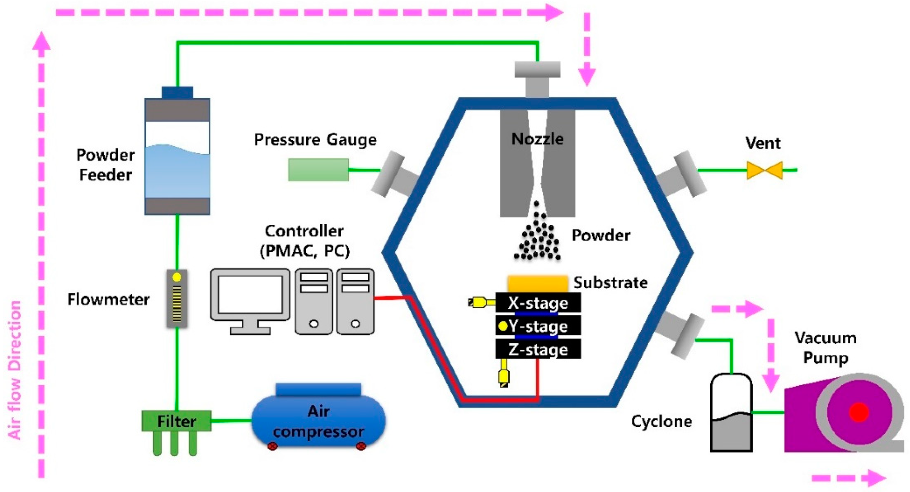
The NPDS consists of a compressor, cylindrical powder feeder, nozzle, vacuum chamber, vacuum pump, vibrator, and controller, as shown in Figure 1. The compressor supplies a compressed air of pressure 0.2 MPa to carry the micro-sized graphite powder from the cylindrical powder feeder to the nozzle which is inside the vacuum chamber. In this research, a slit converging-diverging nozzle of dimensions 50 × 0.2 mm2 was used to accelerate the powder for a large area deposition. A vibrator was used to shake the powder feeder to carry the powder easily to the nozzle. The distance between the nozzle and the stainless-steel substrate was set to be 5 mm. The y-stage is connected to a permanent magnet AC (PMAC) motor to control the scan speed of the substrate. In this study the deposition was carried out directly on a stainless-steel substrate by three different scan speeds without any additional chemical or binders, as shown in Table 1.
2.3. Characterization
The morphology and structure of the deposited film are characterized by field emission scanning electron microscopy (FE-SEM) (JSM-6500F, JEOL, Tokyo, Japan). The crystalline structures of the as-purchased graphite powder and the deposited film on a stainless-steel substrate were examined by XRD (Ultra 4, Rigaku, Tokyo, Japan). Raman Spectra were recorded using Raman spectroscopy (Alpha 300R, WITec GmbH, Ulm, Germany) with a 532 nm wavelength laser operating at 1 mW as an excitation source. Focused ion beam (FIB) (Helios NanoLab 450, FEI, Eindhoven, The Netherlands) milling was carried out to prepare the high-resolution transmission electron microscopy (HR-TEM) sample. A FIB lift-out TEM grid (FIB lift-out Cu TEM grid with 3 posts, Omniprobe, Inc., Dallas, TX, USA) was used to hold the milled HR-TEM sample. Finally, the sample prepared by the FIB was used for HR-TEM (JEM-2100F, JEOL, Tokyo, Japan).
2.4. Preparation of the Polymer Gel Electrolyte
The polymer gel electrolyte was prepared as follows. 1 g of PVA was stirred in 10 mL of deionized water at 80 °C for 2 hours until completely dissolved. After cooling, 0.03 mol (2.94 gm) of H3PO4 were added to the PVA and stirring was continued until the solution became a viscous gel. The sane procedure was followed to prepare 0.06 and 0.09 mol of H3PO4–PVA gel electrolyte by adding 5.88 and 8.82 gm of H3PO4 to the 1 gm of PVA respectively.
2.5. Assembly of Supercapacitor Device
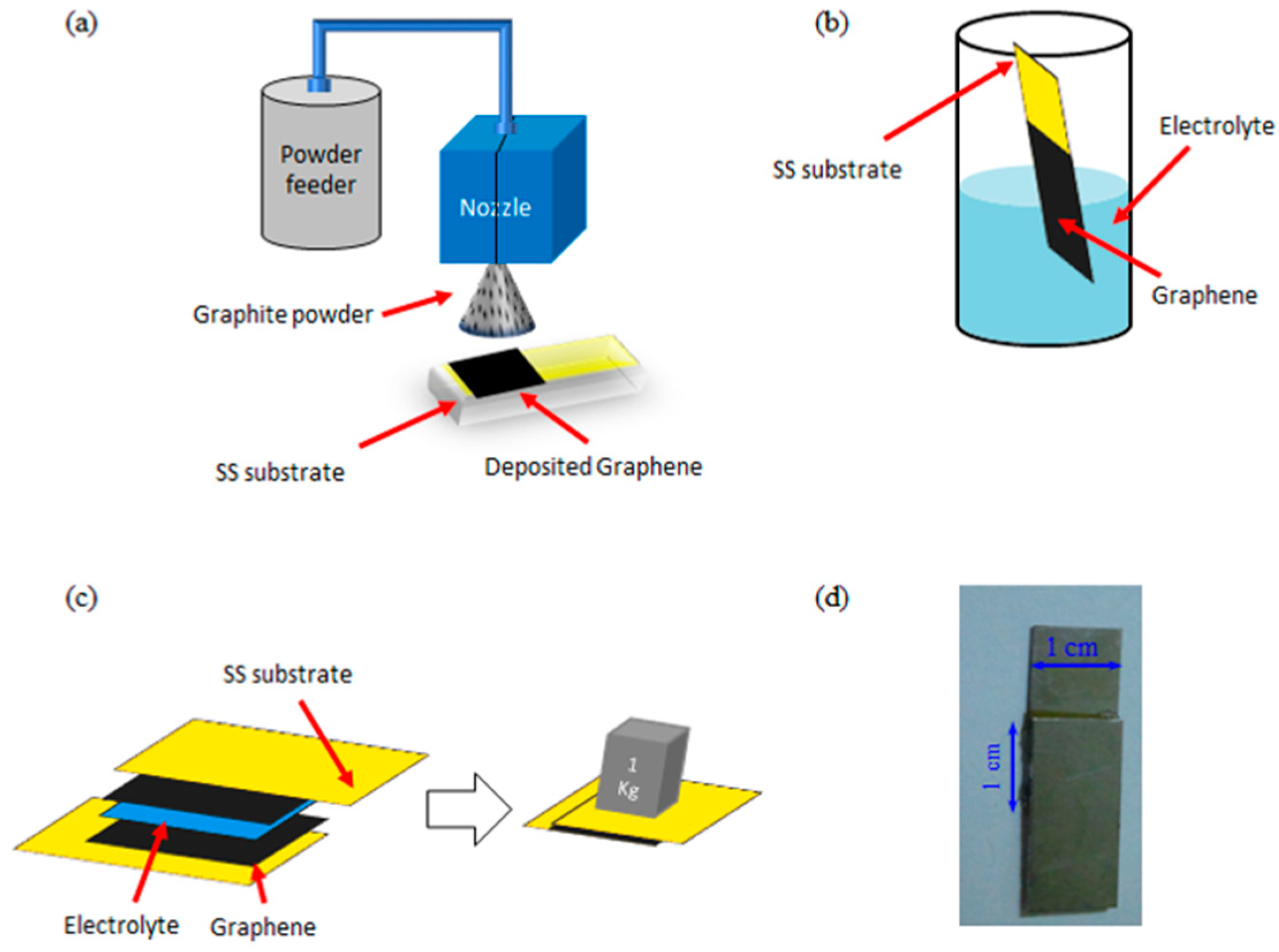
The graphene thin film was deposited on the stainless-steel with area 10 × 10 mm2. To fabricate a supercapacitor, the deposited area was dipped on the H3PO4–PVA gel electrolyte for a minute, the electrolyte on the electrode was left in air overnight to dry. After this, the two identical electrodes with the dried electrolytes were sandwiched together by applying a 1 kg weight, resting on the top, to ensure a full contact. The fabrication process is shown in Figure 2.
2.6. Electrochemical Measurements
The electrochemical properties were measured using a 2-electrode cell. The electrochemical performance was measured using a CorrTest electrochemical workstation (C350, Wuhan Corrtest Instruments Corp. Ltd., Wuhan, China), using cyclic voltammetry, galvanostatic Charge–discharge, and electrochemical impedance spectroscopy. The cyclic voltammetry measurement was scanned between 0 and 1 V with different scan rates between 2 and 100 mV/s. The galvanostatic Charge–discharge tests were performed at different current densities. Impedance data was collected, ranging from 1 MHz to 1 Hz, with an open circuit potential (OCP), with an AC signal 10 mV in amplitude.
3. Results and Discussion
3.1. Morphology Properties
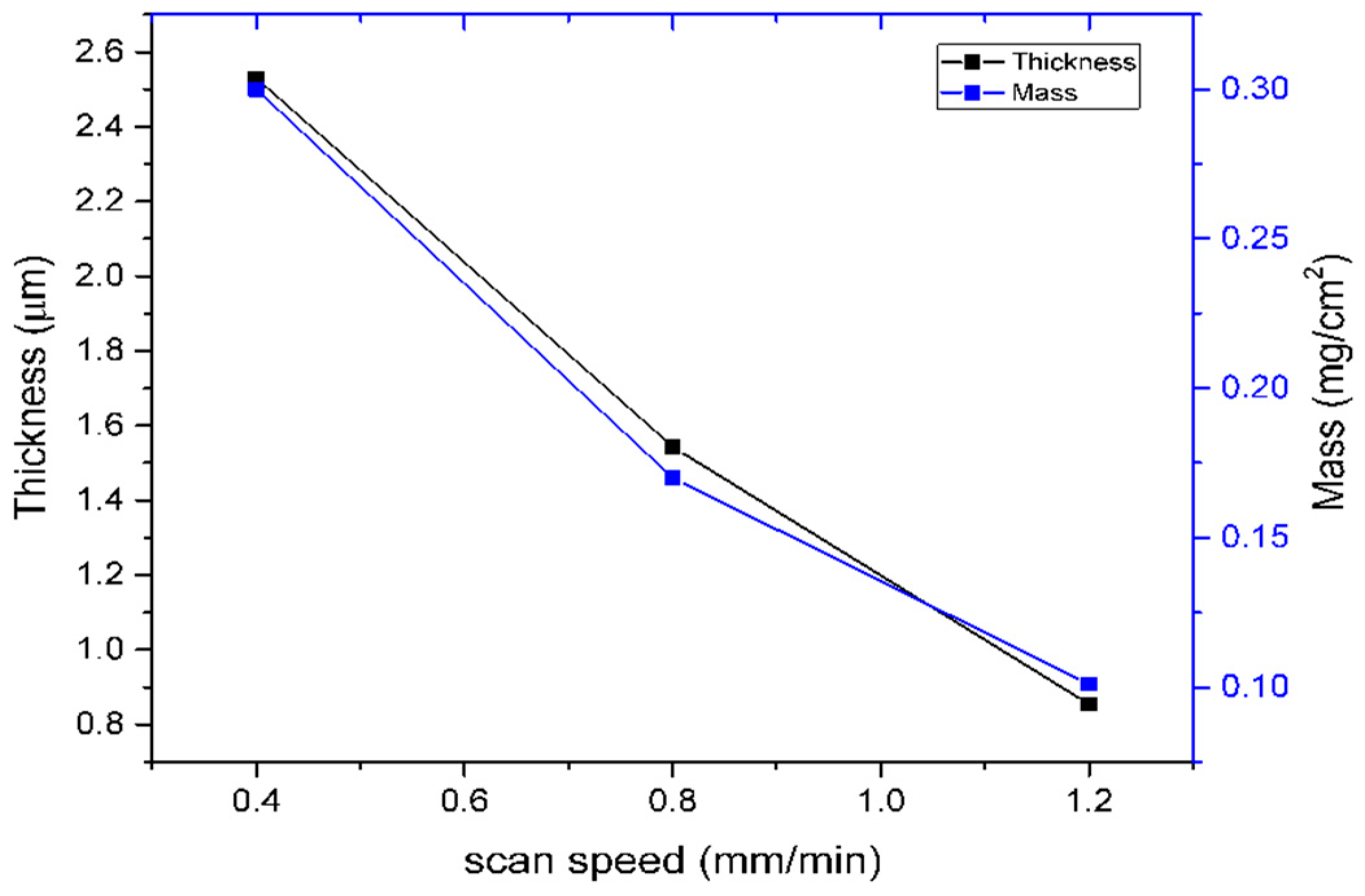
After deposition, the masses per unit area and thicknesses of the deposited films with different scan speeds were calculated. The mass per unit area of the deposited films decreased as the scan speed increased from 0.4 to 0.8 and 1.2 mm/min. The thickness of each deposited film was measured by confocal microscopy, showing that as the scan speed changed from 0.4 to 1.2 mm/min the thickness decreased. The values of mass per unit area and the corresponding thicknesses are shown in Table 2 and Figure 3.
The surface morphology of the original graphite powder and the deposited thin film, on a stainless-steel substrate, was observed with an FE-SEM. Figure 4a is the FE-SEM image of the original graphite powder, showing that the sizes of the original powder particles are around 6 µm and the shapes are irregular. Figure 4b–g shows the surface morphology of the deposited films on stainless steel, by comparing Figure 4a with Figure 4b,c, we can see that most of the graphite powder fragmented to small particles; some of these particles are still in microscale graphite form, but most of the other particles are converted to very small flakes. As seen in Figure 4d–g, as the scan speed increased, the relative proportion of the microscale graphite particles on the deposited films become smaller relative to the slow scan speed case (0.4 mm/min). For 1.2 mm/min scan speed of deposition, the sizes of most of the fragmented particles ranged from about 100–180 nm, however, there were some fragmented particles with much smaller size. In Figure 4c,e,g, red arrows indicate some of the graphene nano-flakes. The thin layers of graphite were separated during the NPDS deposition due to their high impact velocity. The orientation of the particle may be random during deposition, and particles with different orientations collided with the substrate. Due to the high-velocity impact, interlayer sliding and interlayer separation occurred and very thin structures were deposited on the stainless-steel substrate. In addition, large particles broke into small pieces to make nano-sized, thin structures.
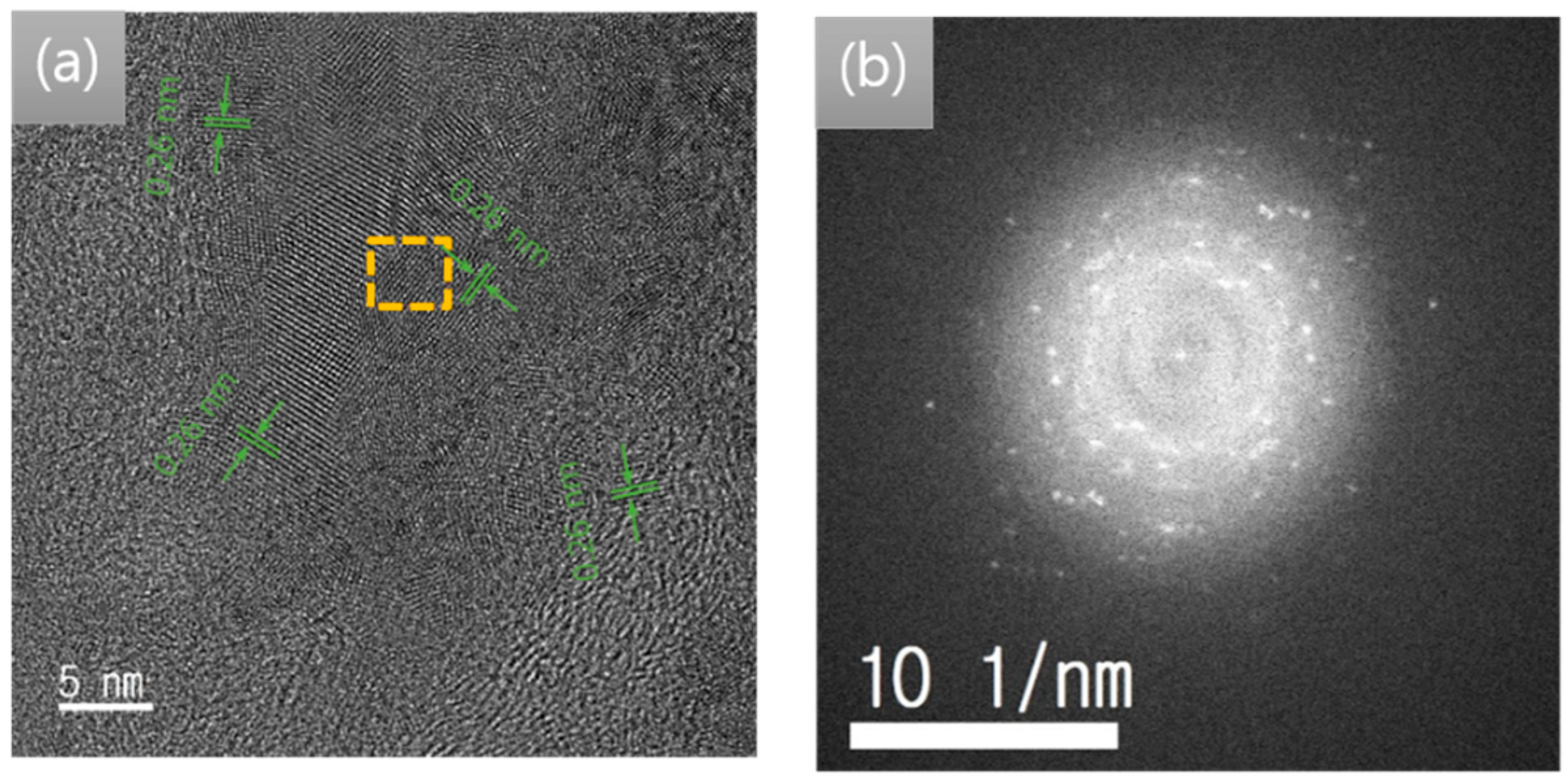
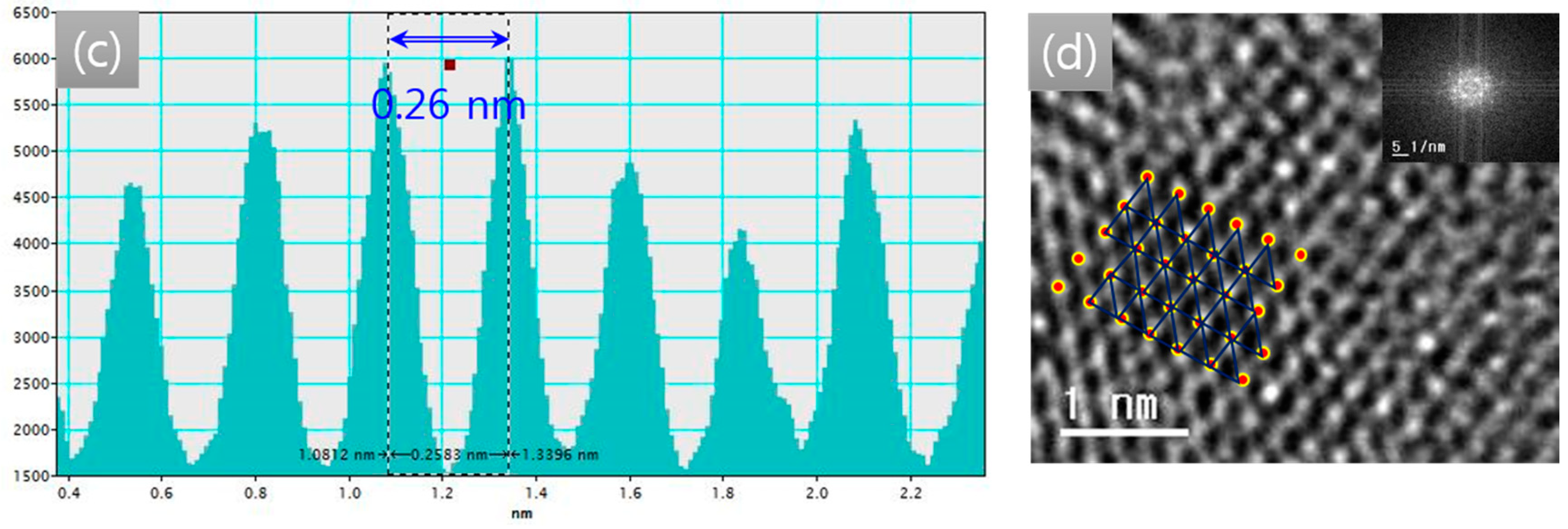
Figure 5 shows the TEM image of the deposited film with a scan speed of 1.2 mm/min. The HR-TEM image shown in Figure 5a indicates the crystalline structure of randomly oriented graphene nano-flakes with some areas of amorphous structure. The Fast Fourier transformer (FFT) of the HR-TEM image in Figure 5b shows a polycrystalline structure which has arisen from the short-range randomly oriented graphene flakes. The obtained histogram plot is shown in Figure 5c at the surrounded position by the yellow rectangle in Figure 5a indicates an in-plane lattice spacing of 0.26 nm corresponding to the graphene lattice spacing [50,51]. Other crystalline areas showed the same lattice spacing of 0.26 nm, as all positions were measured using the histogram plot. This suggests that all crystalline areas are graphene structured. In Figure 5d, the highly magnified image of the surrounded position by the yellow rectangle in Figure 5a shows a triangular sublattice pattern of carbon atoms instead of a hexagonal pattern. This triangular pattern may come from few-layer graphene flake structures [52,53]. The corresponding FFT clearly shows a hexagonal pattern of the graphene structure corresponding to the (100) plane.
3.2. X-ray Diffraction Analysis
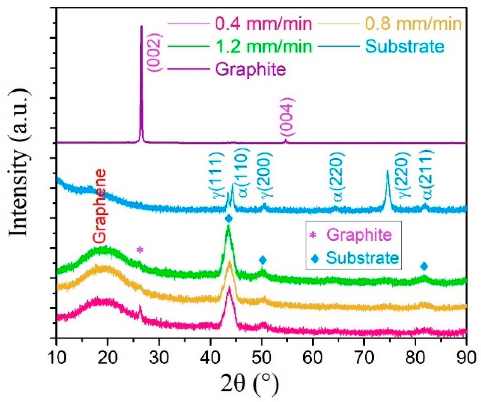
The structural properties of original graphite powder, and the deposited films with different scan speeds (0.4, 0.8, and 1.2 mm/min) and stainless-steel substrate were characterized using XRD analysis. Figure 6 shows the XRD spectrum of the original graphite powder, the sharp and high amplitude peak (002) at 2θ = 26.5°, which is the strongest peak obtained in the diffraction pattern in the direction perpendicular (c-axis) to the graphite hexagonal plates, indicates a highly organized layered structure with an interplanar spacing of 0.365 nm. The XRD spectrum of the deposited films shows peaks γ(111), γ(200), and α(211) at 43.6°, 50.5°, and 82° corresponding to the stainless steel substrate. In the of 0.4 mm/min case, there is (002) graphite peak at 26.3°. This peak disappeared when the scan speed was increased to 0.8 and 1.2 mm/min, which means that the graphene/graphite structure in case of 0.4 mm/min scan speed of deposition transformed to graphene structure as the scan speed increased. Also, the deposited films show a broad carbon (002) peak between 15° and 25°, the broadness of the (002) peak and the shift to a smaller angle indicates a decrease in the particle size due to defragmentation of graphite microparticles to graphene nano-flakes and an increase in the interplanar spacing.
3.3. Raman Spectroscopy
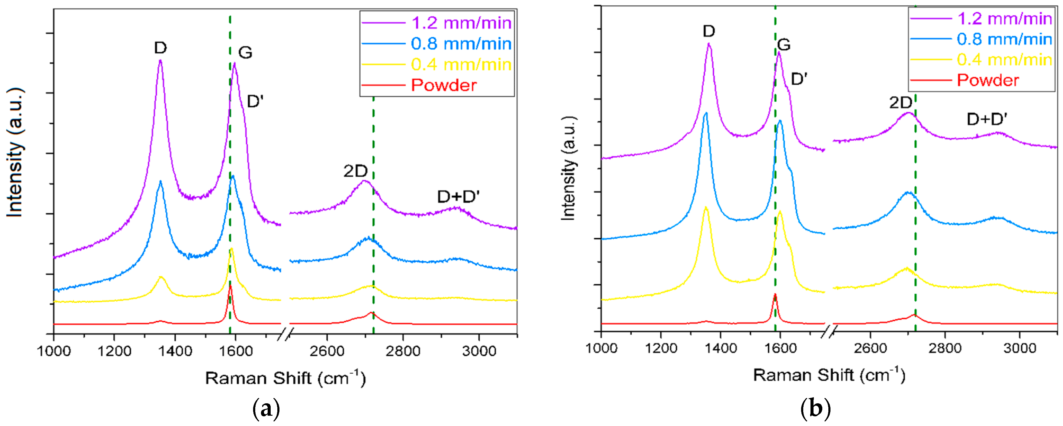
The Raman spectroscopy results of the original graphite powder and deposited films are shown in Figure 7. It is obvious that the graphite powder has mainly three bands, D, G, and 2D, at 1352.4, 1582.1, and 2720.77 cm−1, respectively. The G peak is due to the doubly degenerate zone center E2g mode [54]. The G band has the most intense peak and the D band has negligible intensity. The negligible intensity of the D band suggests a crystalline structure with almost no disorder. The 2D band for graphite consists of two bands 2D1 and 2D2, as shown in the enlarged view of the 2D peak, the double band structure of the 2D peak was explained by other researchers [55,56,57,58,59,60]. For all of the deposited films under all scan speeds (0.4, 0.8 and 1.2 mm/min), the deposited film on stainless steel substrate showed two different behaviors. During measurement, the laser beam was focused in two different positions for a more accurate measurement. When the laser beam was focused on a larger size, fewer fragmented particles were produced, as shown in Figure 7a. In this case, the D peak was located at 1352.4 cm−1 for all deposited films, the G peak positions, for the slower to faster scan speeds, were at 1586, 1592 and 1596 cm−1. We can observe that the ratio of ID/IG, as shown in Table 3, becomes higher when the scan speed of deposition increases, which confirms that the amount of graphite structure on the deposited films decreases as the scan speed of the deposition is increases. 2D peaks appear around 2718, 2708 and 2699 cm−1, respectively for the different scan speeds of deposition. The shift of the G band to a higher energy compared to the graphite powder, the sharpness of 2D peak, and the shift in the 2D band to a lower energy, all indicate that while increasing the scan speed of deposition, more of micro-sized graphite particles gradually transform from graphite to a few-layer graphene structure.
When the laser beam was focused on the fragmented particles, the Raman spectrum of the deposited thin films under all scan speeds (0.4, 0.8 and 1.2 mm/min) has a different interesting behavior; as seen in Figure 7b, the intensity of D band peaks at 1352.4, 1352.4, and 1350.8 cm−1 respectively, which represents the disorder was higher than the G band appears around 1598.5, 1597, and 1595 cm−1, respectively, for the different scan speeds of deposition, which means that the ID/IG for the deposited film is much higher than that of the graphite powder. This increase in ID/IG can be described because of the fragmentation of the micro-sized graphite particles to graphene nano-flakes, which increase the edge defects and disorder of the graphene. The G band is shifted to a higher energy compared to the graphite powder, as shown in Figure 7b. The G band has a shoulder at 1654 cm−1 (D´ band). Also, the 2D band, which appears around 2698 cm−1, for all deposited films, is shifted to lower energy compared to the graphite powder. The 2D band of the deposited film is sharper than that of the original powder. Moreover, the shift in the 2D band indicates that the thickness of the deposited film is decreases after deposition of the original graphite powder on stainless steel using the NPDS. Based on the shifts in the G and 2D peaks, we concluded that the layers of micron-sized graphite powder were separated due to the high impact velocity during deposition, and that few-layer graphene structures have formed on the stainless steel [55,61]. Furthermore, the strong and sharp D band peak and D´ band peak suggest a nanocrystalline structure, as well as the presence of graphene edges and defects [62,63,64]. These graphene edges may appear due to fragmented graphene flake structures. Furthermore, defects may have occurred during the high impact velocity deposition, or by interactions between the stainless steel and graphene, which may have produced vacancies, dislocation, and/or dangling bonds [65]. The positions of the D, G, and 2D peaks for the graphite powder and deposited films are shown in Table 3.
3.4. Electrochemical Properties
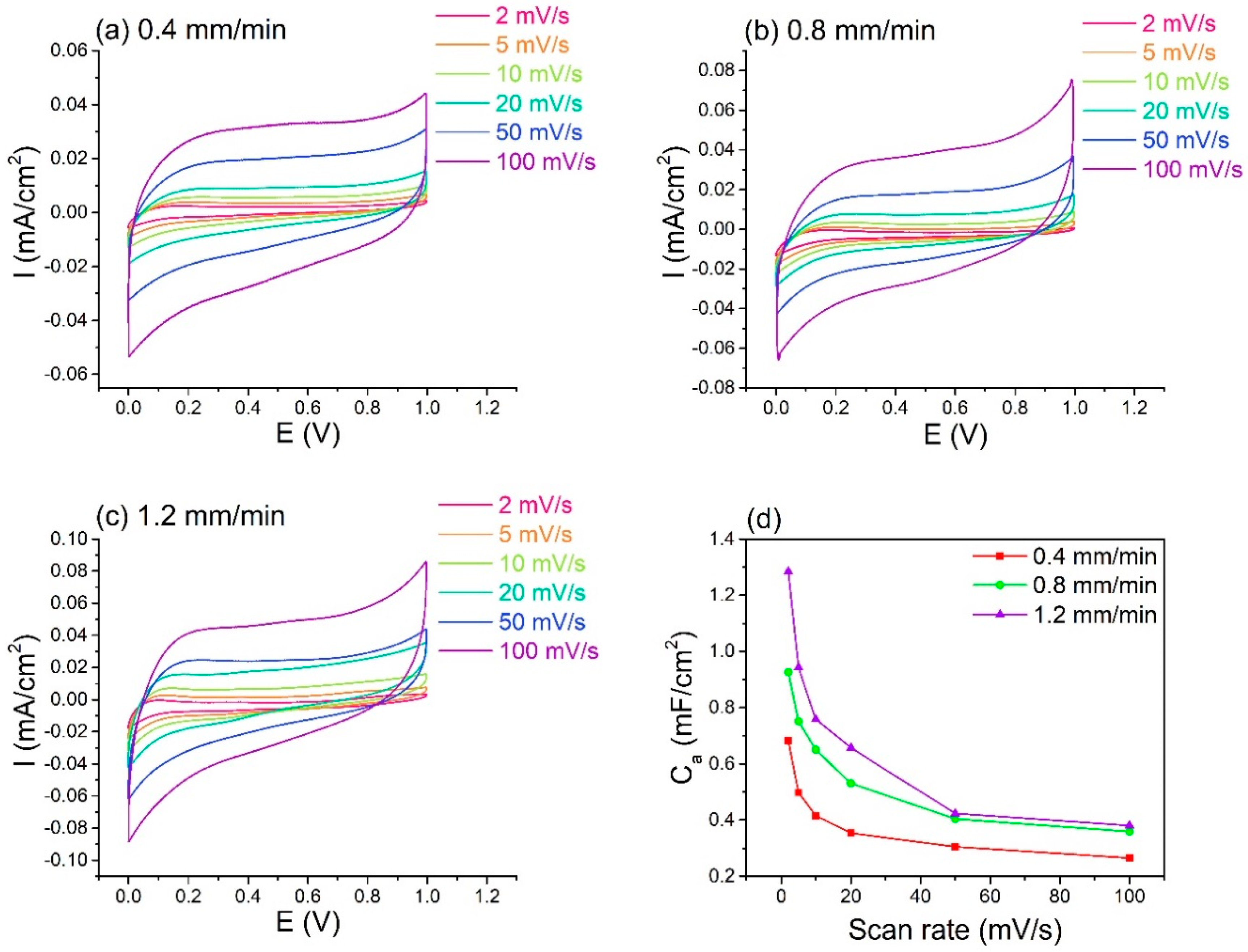
The electrochemical performance of graphene supercapacitors, fabricated from the deposited films (0.4, 0.8 and 1.2 mm/min scan speeds), with the addition of 0.03 mol of H3PO4–PVA gel electrolyte, were investigated as part of a 2-electrode system. Figure 8a–c shows the cyclic voltammetry curves measured at the scan rates 2–100 mV/s and potential window 0–1 V. The areal capacitance calculated from the CV curves using the formula
where I is the response current, s is the scan rate, ΔV is the potential window and A is the area of graphene electrode in contact with the electrolyte. The CV curves of graphene supercapacitor are symmetrical and have a near-rectangular shape over the 1 V potential window, which is typical of an ideal capacitor. The value of areal capacitance was increased from 0.68 mF/cm2 at 2 mV/s for 0.4 mm/min scan speed to 1.28 mF/cm2 at 2 mV/s for 1.2 mm/min scan speed, as shown in Figure 8d, two factors explain this improvement of the capacitance: In case of a fast scan speed, after the graphite particles were accelerated to supersonic speeds through the converging-diverging nozzle, the graphite particles impact with the stainless steel substrate, which has relatively high hardness, so a thin layer of graphene will be formed on the substrate, the deposition quickly will cover another location until it covers the required area of substrate. On the other hand, for the slow scan speed, after the acceleration of graphite powder, the impact takes place at first between the powder and stainless-steel substrate. As in the case of a fast scan speed, a thin graphene layer will form over the substrate, but due to the slow scan speed the impact will happen between the graphite powder and the deposited film, which has a lower hardness than the stainless steel. Therefore, the amount of fragmentation of graphite powders becomes lower than that which occurs with a fast deposition scan speed. This is clear from the (002) graphite peak intensity found in the XRD analysis, which decreased as the scan speed increased. Also, this is clear from the Raman spectroscopy, as previously mentioned. In summary, a slow scan speed shows graphene/graphite structure that has a smaller surface area and lower conductivity than graphene structure in the fast scan speed. As such, the improvement of the capacitance can be explained as a result of two reasons. The first reason is that the graphite structure of the deposited film forms more readily with a slow scan speed deposition, such that the specific surface area becomes higher than in the case of a fast scan speed deposition and allow more charge transfer on the surface of the electrode [66]. The second reason is that the number of graphene layers is decreases with an increase in the scan speed, since the value of ID/IG for a fast scan speed is larger than that of low scan speed and the decreased number of graphene layers can improve the charge transfer inside the electrode material [67,68].
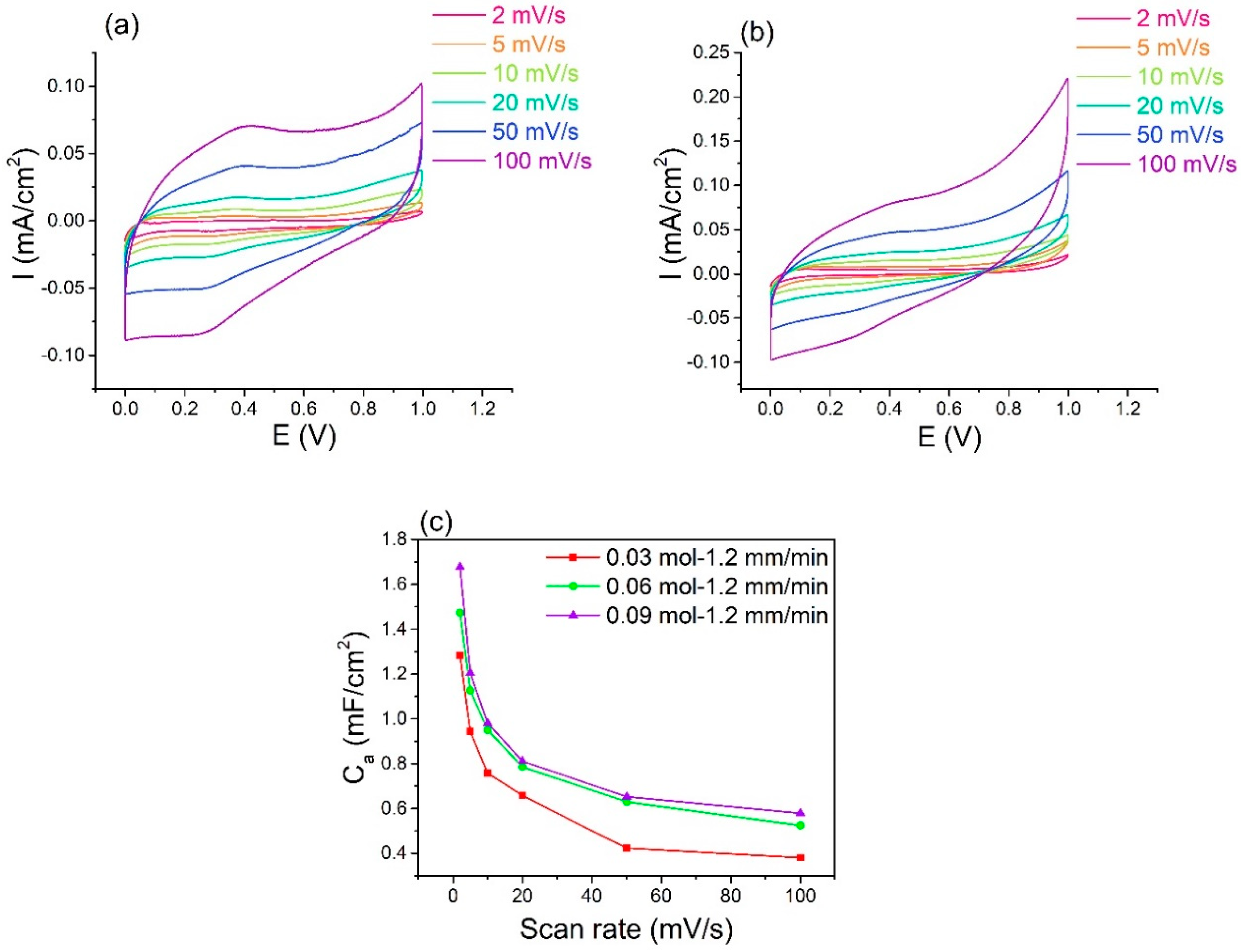
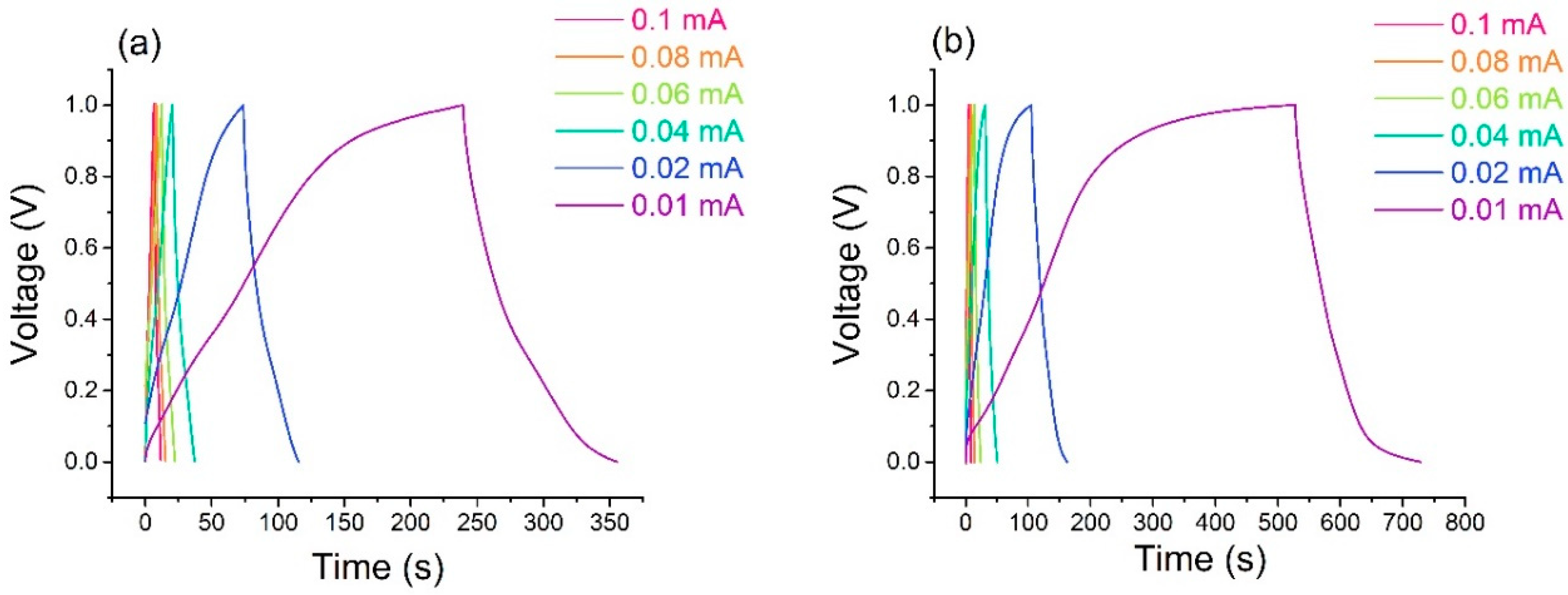
In Figure 9, the cyclic voltammetry was measured again for the deposited films using 0.06 and 0.09 mol H3PO4–PVA gel electrolytes. Both electrolytes have quasi-rectangular CV curves and the areal capacitance was 1.28 mF/cm2 at 2 mV/s for the case of a 1.2 mm/min scan speed with 0.03 mol of H3PO4–PVA gel electrolyte. This value became 1.47 mF/cm2 at 2 mV/s when the concentration of H3PO4 was increased to 0.06 mol and increased to 1.67 mF/cm2 at 2 mV/s for the case of 0.09 mol of H3PO4. It appears that the areal capacitance increases gradually while increasing the concentration in the range of 0.03–0.09 mol. These results confirm the assumption that the high ion concentration cloud improves the areal capacitance value, which also agrees with previous research [69,70]. The capacitance of graphene electrode is mainly due to the diffusion of ions from the electrolyte to the surface of the electrode, and the rate of the whole electrode reaction will be enhanced if the diffusion resistance is decreased. In this sense, a high concentration of H3PO4–PVA gel electrolyte with a high ionic conductivity will provide a low diffusion resistance. The diffusion resistance (Rct: charge transfer resistance) can be seen in the Nyquist plot. Previous studies have also found that there is a relationship between the specific capacitance of the activated carbons and the electrolyte conductivity, i.e., the specific capacitance increased with increasing electrolyte conductivity [71]. For 0.06 mol of H3PO4, the oxidation and reduction peak at ~0.4 and 0.25 V in Figure 9a are corresponding to the pseudocapacitance after phosphorus-doping in graphene layers [72,73,74]. The doping of phosphorus may be happened during the electrochemical measurement due to the porous structure of the carbon atoms. The existence of phosphorus atoms introduces a positive charge on the neighboring carbon atoms and creates centers for oxygen reduction reaction [73]. Also, in case of 0.09 mol of H3PO4, there is a small oxidation and reduction humps at the same potentials due to the same reason. The samples with relatively low concentration of H3PO4 (0.03 mol) did not show the oxidation and reduction peak in the CV curves. Therefore, a relatively high concentration of H3PO4 may easily create the doping of phosphorus during the electrochemical measurement. The reactions related to pseudocapacitance can be considered as follows [75,76]:
The redox reaction attributed to the reversible quinone/hydroquinone pair.
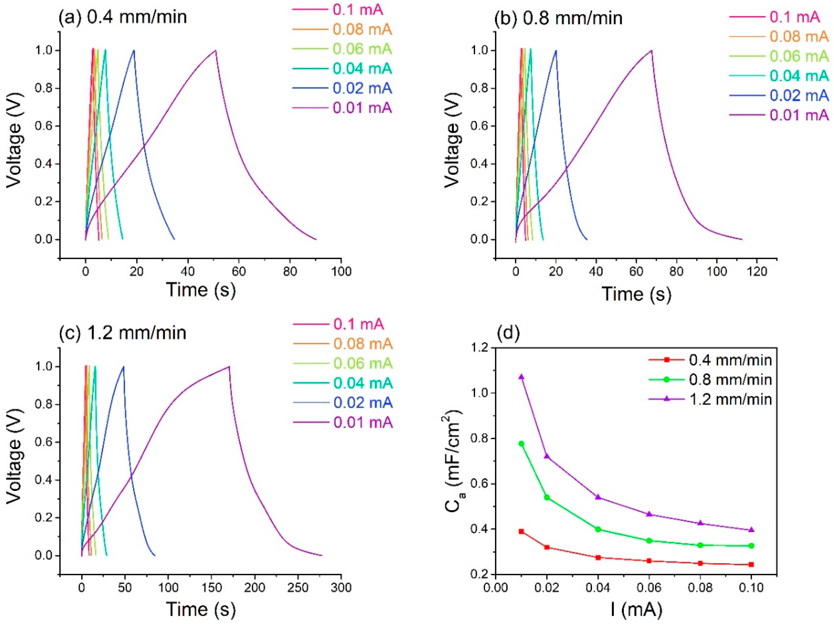
The galvanostatic Charge–discharge curves for the supercapacitors assembled from the deposited films, with different scan speeds (0.4, 0.8 and 1.2 mm/min), in Figure 10a–c, and 0.03, 0.06 and 0.09 mol of H3PO4–PVA gel electrolyte, in Figure 11, were investigated at current densities 0.01–0.1 mA. The areal capacitance was calculated from the CV curves using the formula
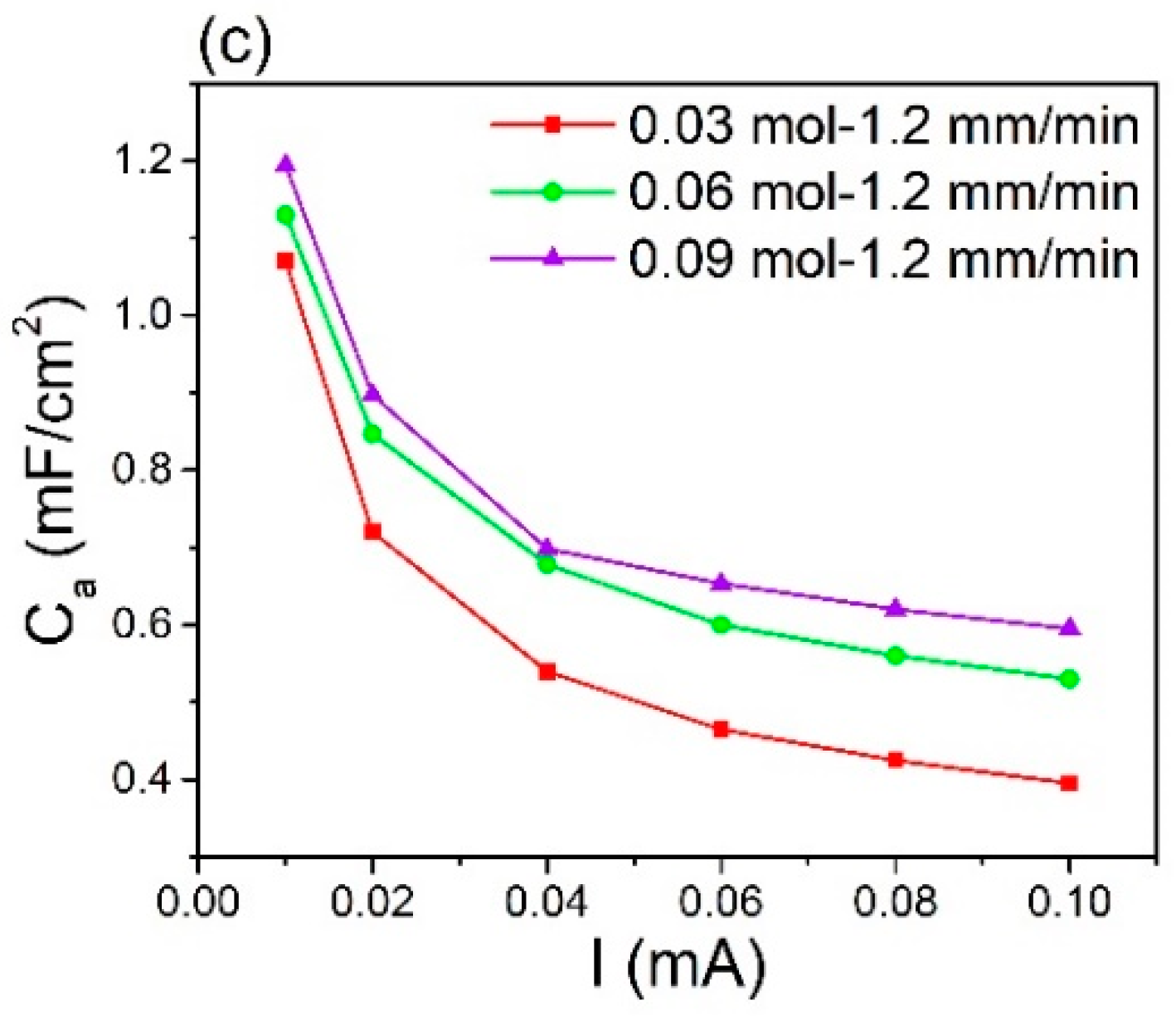
where I is the current density and dV/dt is the slope of discharge curve after the IR drop, where R is the internal resistance of the supercapacitor. Figure 10a–c shows the galvanostatic Charge–discharge curves for all supercapacitors, linear charge and discharge curves with a neglectable IR drop, indicating that the electrodes have a lower internal resistance, which leads to better EDL performance. The areal capacitance calculated from discharge curves is shown in Figure 10d. The results are in agreement with cyclic voltammetry, where the areal capacitance is increased by controlling the thickness of the deposited films by the scan speed of the deposition, for 0.03 mol of H3PO4–PVA gel electrolyte the areal capacitance was 0.39 mF/cm2 for the case of a 0.4 mm/min scan speed. This value increased to 1.07 mF/cm2 when the thickness of the deposited film decreased by increasing the scan speed to 1.2 mm/min. Also increasing the concentration of H3PO4 in the gel electrolyte from 0.03 to 0.09 mol improves the areal capacitance, which increased to 1.2 mF/cm2 for the case of a 1.2 mm/min scan speed with 0.09 mol of H3PO4–PVA gel electrolyte. All areal capacitances are calculated from galvanostatic Charge–discharge at 0.01 mA of current.
Other researchers previously have reported areal capacitances of 3.7 and 2.13 mF/cm2 by CVD [48] and CVD with chemical treatment [77]. The supercapacitor prepared by NPDS shows an areal capacitance 1.67 mF/cm2; even though the value is smaller than those found by other researchers, but the fabrication process is much easier, cheaper, and it can be easily applied in industry because it allows a large area deposition in a small amount of time. The supercapacitor prepared by NPDS is superior to those produced by many other, techniques such as LBL (394 µF/cm2) [78], electrochemical reduction of GO (487 µF/cm2) [45], vertically oriented graphene (0.087 mF/cm2) [79], graphene–CNT carpets (0.23 mF/cm2) [45,80], and graphene–PEDOT: PSS hybrid films (0.179 mF/cm2) [45,81].
Electrochemical impedance spectroscopy (EIS) measurements were carried out to understand the electrochemical details in the frequency range from 1 Hz to 1 MHz with an open-circuit voltage and an AC amplitude of 10 mV.
As shown in Figure 12a, the fabricated supercapacitors from the three electrodes deposited with different scan speed (0.4, 0.8 and 1.2 mm/min) and 0.03 mol H3PO4–PVA all exhibited typical AC impedance characteristics of supercapacitors [82]. In the high-frequency region (Figure 12a enlarge view), the intercept with a real impedance (Z´) represents an equivalent series resistance (Rs), which includes the resistance of electrode materials, ionic resistance of electrolyte, and contact resistance between the electrode and current collector; the radius of semicircle is indicative of the electrode conductivity and the charge-transfer resistance (Rct) of electrode materials. Rs is estimated to be around 1.1 Ω for a 0.4 mm/min scan speed electrode, which was larger than that given by a 0.8 mm/min electrode scan speed (0.97 Ω) and 1.2 mm/min scan speed electrode (0.85 Ω). The semicircle diameter represents the value of Rct obtained for the three electrodes and has a small diameter. This may be due to the formation of graphene-graphite structures on the surface of the 0.4 mm/min scan speed electrode; the amount of this formation may have decreased when the scan speed is increased to 0.8 and 1.2 mm/min, thus improving the impedance of the electrodes. In the intermediate frequency region, the slope of the 45° portion of the curves is the Warburg resistance, which represents the ion diffusion/transport in the electrolyte. In the low-frequency region, the capacitive behavior of the 1.2 mm/min scan speed electrode is evident in the curve. The curve is slightly bent but overall exhibits a good capacitive performance.
Nyquist plots of the three typical 1.2 mm/min scan speed electrodes with 0.03, 0.06 and 0.09 mol H3PO4–PVA electrolytes were measured, as shown in Figure 12b. Rs values were 0.85, 0.62, and 0.42 Ω respectively, the supercapacitor fabricated with 0.09 mol H3PO4–PVA electrolyte exhibits a lower internal resistance and a smaller semicircular diameter at high frequencies, indicating a better interface between the electrolyte and electrode. The conductivity is dependent on the concentration of the H3PO4 in the gel electrolyte; as the H3PO4 concentration increases, the conductivity also increases, meaning the value of Rs decreases as the concentration increases. As a result of increasing the conductivity, mobility of the H3PO4 is increased; this can consequently decrease the value of Rct, which is represented by the radius of semicircle. This result agrees with previous reports [48,83].
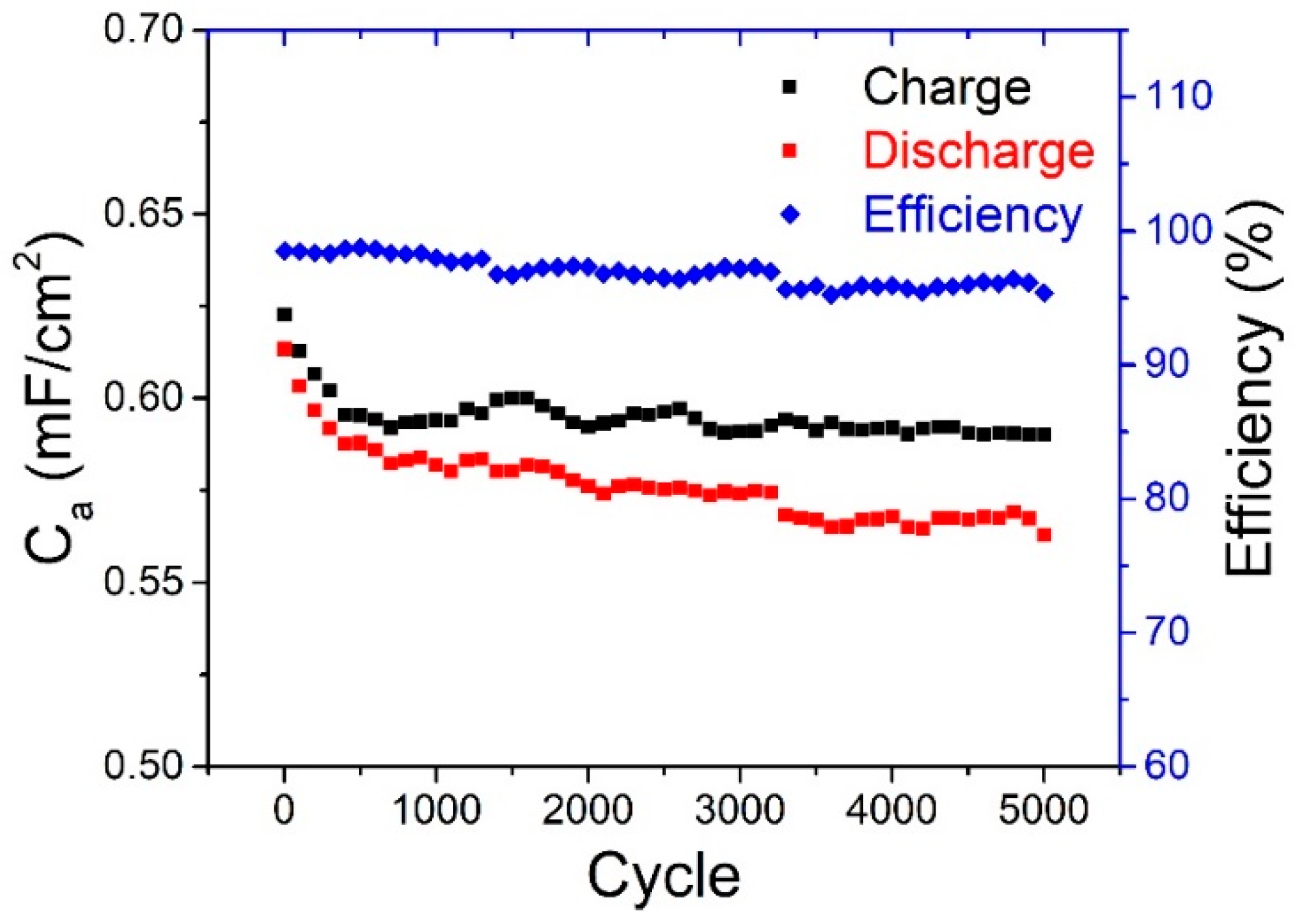
The cyclic stability of the deposited film with a 1.2 mm/min scan speed and 0.09 mol of H3PO4–PVA was investigated at current 0.06 mA, repeating the galvanostatic charge/discharge measurement ranging from 0 to 1 V. As shown in Figure 13, the supercapacitor has a coulombic efficiency of 98% at the beginning, which decreased to 95% after 5000 cycles. The good cycling performance of the electrode material indicated a good stability and strong adherence to the stainless-steel substrate. The good cycling stability can be attributed to two reasons. The first reason is that the few-layer graphene nanoflake structure is randomly oriented on the substrate, which allows the electrolyte ions to diffuse through the graphene layers, leading to a good improvement in the electrochemical performance of the supercapacitor. The second reason is the mechanical stability caused by the strong adherence of the few-layer graphene nanoflake structures on the stainless-steel substrate. The degradation in the coulombic efficiency after 5000 cycles is likely due to the consumption of the electrolyte as a result of irreversible reactions between the graphene electrode and the H3PO4–PVA gel electrolyte.
4. Conclusions
In this research, a vacuum kinetic spray was used to deposit micro-sized graphite powder on stainless steel substrate at room temperature and low-pressure conditions. The NPDS results in the formation of randomly oriented few-layer graphene nano-flakes; as confirmed by FE-SEM, HR-TEM, XRD, and Raman spectroscopy. Some of the graphite particles fragmented to graphene nano-flakes and some particles did not fragment and were converted to graphite particles with a smaller size than the particles in the original graphite powder. The amount of graphite structure on the deposited films decreases with an increase in the deposition scan speed.
The electrochemical capacitive behavior of the supercapacitors assembled from the deposited films using NPDS, with 0.03 mol PVA-H3PO4, showed an areal capacitance comparable to other research, and it was improved by increasing the scan speed of the deposition. Also, increasing the amount of H3PO4 in the PVA gel electrolyte can improve the areal capacitance. The very affordably fabricated supercapacitor with 0.09 mol H3PO4–PVA gel electrolyte, produced with a 1.2 mm/min deposition scan speed, showed a good stability over 5000 cycles.
Author Contributions
Conceptualization, D.-M.C. and M.M.M.M.; Methodology, M.M.M.M.; Formal Analysis, M.M.M.M.; Investigation, M.M.M.M.; Resources, D.-M.C.; Data Curation, M.M.M.M.; Writing–Original Draft Preparation, M.M.M.M.; Writing–Review & Editing, D.-M.C. and M.M.M.M.; Visualization, M.M.M.M.; Supervision, D.-M.C.; Project Administration, D.-M.C.; Funding Acquisition, D.-M.C.
Funding
This research was supported by a National Research Foundation of Korea (NRF) (NRF-2018R1A2B6004012), Nano-Convergence Foundation (www.nanotech2020.org), and the Ministry of Science and ICT (MSIT, Korea) & Ministry of Trade, Industry and Energy (MOTIE, Korea) (Project name: Establishment of Battery/Ess-Based Energy Industry Innovation Ecosystem).
Conflicts of Interest
The authors declare no conflicts of interest.
References
- Miller, J.R.; Simon, P. Electrochemical capacitors for energy management. Science 2008, 321, 651–652. [Google Scholar] [CrossRef] [PubMed] [Green Version]
- Simon, P.; Gogotsi, Y. Materials for electrochemical capacitors. Nat. Mater. 2008, 7, 845–854. [Google Scholar] [CrossRef] [PubMed]
- Liu, C.; Li, F.; Ma, L.-P.; Cheng, H.-M. Advanced materials for energy storage. Adv. Mater. 2010, 22, E28–E62. [Google Scholar] [CrossRef] [PubMed]
- Kötz, R.; Carlen, M. Principles and applications of electrochemical capacitors. Electrochim. Acta 2000, 45, 2483–2498. [Google Scholar] [CrossRef]
- Kaempgen, M.; Chan, C.K.; Ma, J.; Cui, Y.; Gruner, G. Printable thin film supercapacitors using single-walled carbon nanotubes. Nano Lett. 2009, 9, 1872–1876. [Google Scholar] [CrossRef] [PubMed]
- Shakir, I. High energy density based flexible electrochemical supercapacitors from layer-by-layer assembled multiwall carbon nanotubes and graphene. Electrochim. Acta 2014, 129, 396–400. [Google Scholar] [CrossRef]
- Geim, A.K.; Novoselov, K.S. The rise of graphene. Nat. Mater. 2007, 6, 183–191. [Google Scholar] [CrossRef] [PubMed]
- Geim, A.K. Graphene: Status and prospects. Science 2009, 324, 1530–1534. [Google Scholar] [CrossRef] [PubMed]
- Novoselov, K.S.; Geim, A.K.; Morozov, S.V.; Jiang, D.; Katsnelson, M.I.; Grigorieva, I.V.; Dubonos, S.V.; Firsov, A.A. Two-dimensional gas of massless Dirac fermions in graphene. Nature 2005, 438, 197–200. [Google Scholar] [CrossRef] [PubMed] [Green Version]
- Peigney, A.; Laurent, C.; Flahaut, E.; Bacsa, R.R.; Rousset, A. Specific surface area of carbon nanotubes and bundles of carbon nanotubes. Carbon 2001, 39, 507–514. [Google Scholar] [CrossRef] [Green Version]
- El-Kady, M.F.; Strong, V.; Dubin, S.; Kaner, R.B. Laser scribing of high-performance and flexible graphene-based electrochemical capacitors. Science 2012, 335, 1326–1330. [Google Scholar] [CrossRef] [PubMed]
- Abdelkader, A.M.; Karim, N.; Vallés, C.; Afroj, S.; Novoselov, K.S.; Yeates, S.G. Ultraflexible and robust graphene supercapacitors printed on textiles for wearable electronics applications. 2D Mater. 2017, 4, 035016. [Google Scholar] [CrossRef] [Green Version]
- Abdelkader, A.M.; Fray, D.J. Controlled electrochemical doping of graphene-based 3D nanoarchitecture electrodes for supercapacitors and capacitive deionisation. Nanoscale 2017, 9, 14548–14557. [Google Scholar] [CrossRef] [PubMed]
- Wu, Q.; Xu, Y.; Yao, Z.; Liu, A.; Shi, G. Supercapacitors based on flexible graphene/polyaniline nanofiber composite films. ACS Nano 2010, 4, 1963–1970. [Google Scholar] [CrossRef] [PubMed]
- Zhu, Y.; Murali, S.; Stoller, M.D.; Ganesh, K.; Cai, W.; Ferreira, P.J.; Pirkle, A.; Wallace, R.; Cychosz, K.A.; Thommes, M.; et al. Carbon-based supercapacitors produced by activation of graphene. Science 2011, 332, 1537–1541. [Google Scholar] [CrossRef] [PubMed]
- Wei, J.; Zang, Z.; Zhang, Y.; Wang, M.; Du, J.; Tang, X. Enhanced performance of light-controlled conductive switching in hybrid cuprous oxide/reduced graphene oxide (Cu2O/rGO) nanocomposites. Opt. Lett. 2017, 42, 911–914. [Google Scholar] [CrossRef] [PubMed]
- Huang, H.; Zhang, J.; Jiang, L.; Zang, Z. Preparation of cubic Cu2O nanoparticles wrapped by reduced graphene oxide for the efficient removal of rhodamine B. J. Alloys Compd. 2017, 718, 112–115. [Google Scholar] [CrossRef]
- Zang, Z.; Zeng, X.; Wang, M.; Hu, W.; Liu, C.; Tang, X. Tunable photoluminescence of water-soluble AgInZnS–graphene oxide (GO) nanocomposites and their application in-vivo bioimaging. Sens. Actuators B Chem. 2017, 252, 1179–1186. [Google Scholar] [CrossRef]
- Dikin, D.A.; Stankovich, S.; Zimney, E.J.; Piner, R.D.; Dommett, G.H.B.; Evmenenko, G.; Nguyen, S.T.; Ruoff, R.S. Preparation and characterization of graphene oxide paper. Nature 2007, 448, 457–460. [Google Scholar] [CrossRef] [PubMed]
- Segal, M. Selling graphene by the ton. Nat. Nanotechnol. 2009, 4, 612–614. [Google Scholar] [CrossRef] [PubMed]
- Wu, Z.-S.; Wang, D.-W.; Ren, W.; Zhao, J.; Zhou, G.; Li, F.; Cheng, H.-M. Anchoring hydrous RuO2 on Graphene sheets for high-performance electrochemical capacitors. Adv. Funct. Mater. 2010, 20, 3595–3602. [Google Scholar] [CrossRef]
- Novoselov, K.S.; Geim, A.K.; Morozov, S.V.; Jiang, D.; Zhang, Y.; Dubonos, S.V.; Grigorieva, I.V.; Firsov, A.A. Electric Field effect in atomically thin carbon films. Science 2004, 306, 666–669. [Google Scholar] [CrossRef] [PubMed]
- Singh, V.; Joung, D.; Zhai, L.; Das, S.; Khondaker, S.I.; Seal, S. Graphene based materials: Past, present and future. Prog. Mater. Sci. 2011, 56, 1178–1271. [Google Scholar] [CrossRef]
- Park, S.; Ruoff, R.S. Chemical methods for the production of graphenes. Nat. Nanotechnol. 2009, 4, 217–224. [Google Scholar] [CrossRef] [PubMed]
- Ambrosi, A.; Pumera, M. Electrochemically exfoliated graphene and graphene oxide for energy storage and electrochemistry applications. Chem. A Eur. J. 2016, 22, 153–159. [Google Scholar] [CrossRef] [PubMed]
- Chen, C.-H.; Yang, S.-W.; Chuang, M.-C.; Woon, W.-Y.; Su, C.-Y. Towards the continuous production of high crystallinity graphene via electrochemical exfoliation with molecular in situ encapsulation. Nanoscale 2015, 7, 15362–15373. [Google Scholar] [CrossRef] [PubMed]
- Abdelkader, A.M.; Cooper, A.J.; Dryfe, R.A.W.; Kinloch, I.A. How to get between the sheets: A review of recent works on the electrochemical exfoliation of graphene materials from bulk graphite. Nanoscale 2015, 7, 6944–6956. [Google Scholar] [CrossRef] [PubMed]
- Ossonon, B.D.; Bélanger, D. Functionalization of graphene sheets by the diazonium chemistry during electrochemical exfoliation of graphite. Carbon 2017, 111, 83–93. [Google Scholar] [CrossRef]
- Yang, S.; Brüller, S.; Wu, Z.-S.; Liu, Z.; Parvez, K.; Dong, R.; Richard, F.; Samorì, P.; Feng, X.; Müllen, K. Organic Radical-assisted electrochemical exfoliation for the scalable production of high-quality graphene. J. Am. Chem. Soc. 2015, 137, 13927–13932. [Google Scholar] [CrossRef] [PubMed]
- Hernandez, Y.; Nicolosi, V.; Lotya, M.; Blighe, F.M.; Sun, Z.; De, S.; McGovern, I.T.; Holland, B.; Byrne, M.; Gun’Ko, Y.K.; et al. High-yield production of graphene by liquid-phase exfoliation of graphite. Nat. Nanotechnol. 2008, 3, 563–568. [Google Scholar] [CrossRef] [PubMed] [Green Version]
- Behabtu, N.; Lomeda, J.R.; Green, M.J.; Higginbotham, A.L.; Sinitskii, A.; Kosynkin, D.V.; Tsentalovich, D.; Parra-Vasquez, A.N.G.; Schmidt, J.; Kesselman, E.; et al. Spontaneous high-concentration dispersions and liquid crystals of graphene. Nat. Nanotechnol. 2010, 5, 406–411. [Google Scholar] [CrossRef] [PubMed]
- Sun, Y.; Wu, Q.; Shi, G. Graphene based new energy materials. Energy Environ. Sci. 2011, 4, 1113–1132. [Google Scholar] [CrossRef]
- Ferrari, A.C.; Bonaccorso, F.; Fal’ko, V.; Novoselov, K.S.; Roche, S.; Boggild, P.; Borini, S.; Koppens, F.H.L.; Palermo, V.; Pugno, N.; et al. Science and technology roadmap for graphene, related two-dimensional crystals, and hybrid systems. Nanoscale 2015, 7, 4598–4810. [Google Scholar] [CrossRef] [PubMed] [Green Version]
- Reina, A.; Jia, X.; Ho, J.; Nezich, D.; Son, H.; Bulovic, V.; Dresselhaus, M.S.; Kong, J. Large area, few-layer graphene films on arbitrary substrates by chemical vapor deposition. Nano Lett. 2009, 9, 30–35. [Google Scholar] [CrossRef] [PubMed]
- Bae, S.; Kim, H.; Lee, Y.; Xu, X.; Park, J.-S.; Zheng, Y.; Balakrishnan, J.; Lei, T.; Kim, H.R.; Song, Y.I.; et al. Roll-to-roll production of 30-inch graphene films for transparent electrodes. Nat. Nanotechnol. 2010, 5, 574–578. [Google Scholar] [CrossRef] [PubMed] [Green Version]
- Cai, W.; Moore, A.L.; Zhu, Y.; Li, X.; Chen, S.; Shi, L.; Ruoff, R.S. Thermal transport in suspended and supported monolayer graphene grown by chemical vapor deposition. Nano Lett. 2010, 10, 1645–1651. [Google Scholar] [CrossRef] [PubMed]
- Cai, W.; Piner, R.D.; Zhu, Y.; Li, X.; Tan, Z.; Floresca, H.C.; Yang, C.; Lu, L.; Kim, M.J.; Ruoff, R.S. Synthesis of isotopically-labeled graphite films by cold-wall chemical vapor deposition and electronic properties of graphene obtained from such films. Nano Res. 2009, 2, 851. [Google Scholar] [CrossRef]
- Fallahazad, B.; Hao, Y.; Lee, K.; Kim, S.; Ruoff, R.S.; Tutuc, E. Quantum hall effect in Bernal stacked and twisted bilayer graphene grown on Cu by chemical vapor deposition. Phys. Rev. B 2012, 85, 201408. [Google Scholar] [CrossRef]
- Li, X.; Magnuson, C.W.; Venugopal, A.; Tromp, R.M.; Hannon, J.B.; Vogel, E.M.; Colombo, L.; Ruoff, R.S. Large-area graphene single crystals grown by low-pressure chemical vapor deposition of methane on copper. J. Am. Chem. Soc. 2011, 133, 2816–2819. [Google Scholar] [CrossRef] [PubMed]
- Suk, J.W.; Kitt, A.; Magnuson, C.W.; Hao, Y.; Ahmed, S.; An, J.; Swan, A.K.; Goldberg, B.B.; Ruoff, R.S. Transfer of CVD-grown monolayer graphene onto arbitrary substrates. ACS Nano 2011, 5, 6916–6924. [Google Scholar] [CrossRef] [PubMed]
- Allen, M.J.; Tung, V.C.; Kaner, R.B. Honeycomb carbon: A review of graphene. Chem. Rev. 2010, 110, 132–145. [Google Scholar] [CrossRef] [PubMed]
- Chun, D.M.; Kim, M.H.; Lee, J.C.; Ahn, S.H. TiO2 coating on metal and polymer substrates by nano-particle deposition system (NPDS). CIRP Ann. Manuf. Technol. 2008, 57, 551–554. [Google Scholar] [CrossRef]
- Chun, D.-M.; Kim, M.-H.; Lee, J.-C.; Ahn, S.-H. A nano-particle deposition system for ceramic and metal coating at room temperature and low vacuum conditions. Int. J. Precis. Eng. Manuf. 2008, 9, 51–53. [Google Scholar]
- Jung, K.; Song, W.; Chun, D.-M.; Kim, Y.-H.; Yeo, J.-C.; Kim, M.-S.; Ahn, S.-H.; Lee, C.-S. Nickel line patterning using silicon supersonic micronozzle integrated with a nanoparticle deposition system. Jpn. J. Appl. Phys. 2010, 49, 05EC09. [Google Scholar] [CrossRef]
- Sheng, K.; Sun, Y.; Li, C.; Yuan, W.; Shi, G. Ultrahigh-rate supercapacitors based on eletrochemically reduced graphene oxide for ac line-filtering. Sci. Rep. 2012, 2, 247. [Google Scholar] [CrossRef] [PubMed]
- Nasim, M.N.E.A.A.; Chun, D.-M. Formation of few-layer graphene flake structures from graphite particles during thin film coating using dry spray deposition method. Thin Solid Films 2017, 622, 34–40. [Google Scholar] [CrossRef]
- Nasim, M.N.E.A.A.; Chun, D.-M. Substrate-dependent deposition behavior of graphite particles dry-sprayed at room temperature using a nano-particle deposition system. Surf. Coat. Technol. 2017, 309, 172–178. [Google Scholar] [CrossRef]
- Chen, Q.; Li, X.; Zang, X.; Cao, Y.; He, Y.; Li, P.; Wang, K.; Wei, J.; Wu, D.; Zhu, H. Effect of different gel electrolytes on graphene-based solid-state supercapacitors. RSC Adv. 2014, 4, 36253–36256. [Google Scholar] [CrossRef]
- Li, S.; Wang, X.; Xing, H.; Shen, C. Micro supercapacitors based on a 3D structure with symmetric graphene or activated carbon electrodes. J. Micromech. Microeng. 2013, 23, 114013. [Google Scholar] [CrossRef]
- Yu, K.; Zhao, W.; Wu, X.; Zhuang, J.; Hu, X.; Zhang, Q.; Sun, J.; Xu, T.; Chai, Y.; Ding, F.; et al. In situ atomic-scale observation of monolayer graphene growth from SiC. Nano Res. 2018, 11, 2809–2820. [Google Scholar] [CrossRef]
- Muthurasu, A.; Dhandapani, P.; Ganesh, V. Facile and simultaneous synthesis of graphene quantum dots and reduced graphene oxide for bio-imaging and supercapacitor applications. New J. Chem. 2016, 40, 9111–9124. [Google Scholar] [CrossRef]
- Kumar, G.S.; Thupakula, U.; Sarkar, P.K.; Acharya, S. Easy extraction of water-soluble graphene quantum dots for light emitting diodes. RSC Adv. 2015, 5, 27711–27716. [Google Scholar] [CrossRef]
- Robertson, A.W.; Warner, J.H. Atomic resolution imaging of graphene by transmission electron microscopy. Nanoscale 2013, 5, 4079–4093. [Google Scholar] [CrossRef] [PubMed]
- Tuinstra, F.; Koenig, J.L. Raman spectrum of graphite. J. Chem. Phys. 1970, 53, 1126–1130. [Google Scholar] [CrossRef]
- Ferrari, A.C. Raman spectroscopy of graphene and graphite: Disorder, electron–phonon coupling, doping and nonadiabatic effects. Solid State Commun. 2007, 143, 47–57. [Google Scholar] [CrossRef]
- Cançado, L.G.; Pimenta, M.A.; Neves, B.R.A.; Medeiros-Ribeiro, G.; Enoki, T.; Kobayashi, Y.; Takai, K.; Fukui, K.; Dresselhaus, M.S.; Saito, R.; et al. Anisotropy of the Raman spectra of nanographite ribbons. Phys. Rev. Lett. 2004, 93, 047403. [Google Scholar] [CrossRef] [PubMed]
- Nemanich, R.J.; Solin, S.A. First- and second-order Raman scattering from finite-size crystals of graphite. Phys. Rev. B 1979, 20, 392–401. [Google Scholar] [CrossRef]
- Vidano, R.P.; Fischbach, D.B.; Willis, L.J.; Loehr, T.M. Observation of Raman band shifting with excitation wavelength for carbons and graphites. Solid State Commun. 1981, 39, 341–344. [Google Scholar] [CrossRef]
- Pócsik, I.; Hundhausen, M.; Koós, M.; Ley, L. Origin of the D peak in the Raman spectrum of microcrystalline graphite. J. Non Cryst. Solids 1998, 227, 1083–1086. [Google Scholar] [CrossRef]
- Maultzsch, J.; Reich, S.; Thomsen, C.; Requardt, H.; Ordejón, P. Phonon dispersion in graphite. Phys. Rev. Lett. 2004, 92, 075501. [Google Scholar] [CrossRef] [PubMed]
- Wang, H.; Wang, Y.; Cao, X.; Feng, M.; Lan, G. Vibrational properties of graphene and graphene layers. J. Raman Spectrosc. 2009, 40, 1791–1796. [Google Scholar] [CrossRef]
- Hiramatsu, M.; Shiji, K.; Amano, H.; Hori, M. Fabrication of vertically aligned carbon nanowalls using capacitively coupled plasma-enhanced chemical vapor deposition assisted by hydrogen radical injection. Appl. Phys. Lett. 2004, 84, 4708–4710. [Google Scholar] [CrossRef]
- Hiramatsu, M.; Hori, M. Fabrication of carbon nanowalls using novel plasma processing. Jpn. J. Appl. Phys. 2006, 45, 5522. [Google Scholar] [CrossRef]
- Mori, T.; Hiramatsu, M.; Yamakawa, K.; Takeda, K.; Hori, M. Fabrication of carbon nanowalls using electron beam excited plasma-enhanced chemical vapor deposition. Diam. Relat. Mater. 2008, 17, 1513–1517. [Google Scholar] [CrossRef]
- Ni, Z.; Wang, Y.; Yu, T.; Shen, Z. Raman spectroscopy and imaging of graphene. Nano Res. 2008, 1, 273–291. [Google Scholar] [CrossRef] [Green Version]
- Wang, M.; Liu, Q.; Sun, H.; Stach, E.A.; Zhang, H.; Stanciu, L.; Xie, J. Preparation of high-surface-area carbon nanoparticle/graphene composites. Carbon 2012, 50, 3845–3853. [Google Scholar] [CrossRef]
- Liu, J.; Notarianni, M.; Will, G.; Tiong, V.T.; Wang, H.; Motta, N. Electrochemically exfoliated graphene for electrode films: effect of graphene flake thickness on the sheet resistance and capacitive properties. Langmuir 2013, 29, 13307–13314. [Google Scholar] [CrossRef] [PubMed] [Green Version]
- Galindo, B.; Alcolea, S.G.; Gómez, J.; Navas, A.; Murguialday, A.O.; Fernandez, M.P.; Puelles, R.C. Effect of the number of layers of graphene on the electrical properties of TPU polymers. IOP Conf. Ser. Mater. Sci. Eng. 2014, 64, 012008. [Google Scholar] [CrossRef] [Green Version]
- Srinivasan, V.; Weidner, J.W. Studies on the capacitance of nickel oxide films: effect of heating temperature and electrolyte concentration. J. Electrochem. Soc. 2000, 147, 880–885. [Google Scholar] [CrossRef]
- Zheng, J.P.; Jow, T.R. The effect of salt concentration in electrolytes on the maximum energy storage for double layer capacitors. J. Electrochem. Soc. 1997, 144, 2417–2420. [Google Scholar] [CrossRef]
- Torchała, K.; Kierzek, K.; Machnikowski, J. Capacitance behavior of KOH activated mesocarbon microbeads in different aqueous electrolytes. Electrochim. Acta 2012, 86, 260–267. [Google Scholar] [CrossRef]
- Yu, X.; Kim, H.J.; Hong, J.-Y.; Jung, Y.M.; Kwon, K.D.; Kong, J.; Park, H.S. Elucidating surface redox charge storage of phosphorus-incorporated graphenes with hierarchical architectures. Nano Energy 2015, 15, 576–586. [Google Scholar] [CrossRef]
- Wen, Y.; Wang, B.; Huang, C.; Wang, L.; Hulicova-Jurcakova, D. Synthesis of phosphorus-doped graphene and its wide potential window in aqueous supercapacitors. Chem. A Eur. J. 2014, 21, 80–85. [Google Scholar] [CrossRef] [PubMed]
- Thirumal, V.; Pandurangan, A.; Jayavel, R.; Venkatesh, K.S.; Palani, N.S.; Ragavan, R.; Ilangovan, R. Single pot electrochemical synthesis of functionalized and phosphorus doped graphene nanosheets for supercapacitor applications. J. Mater. Sci. Mater. Electron. 2015, 26, 6319–6328. [Google Scholar] [CrossRef]
- Pan, H.; Poh, C.K.; Feng, Y.P.; Lin, J. Supercapacitor electrodes from tubes-in-tube carbon nanostructures. Chem. Mater. 2007, 19, 6120–6125. [Google Scholar] [CrossRef]
- Xie, B.; Chen, Y.; Yu, M.; Zhang, S.; Lu, L.; Shu, Z.; Zhang, Y. Phosphoric acid-assisted synthesis of layered MoS2/graphene hybrids with electrolyte-dependent supercapacitive behaviors. RSC Adv. 2016, 6, 89397–89406. [Google Scholar] [CrossRef]
- Li, X.; Zhao, T.; Chen, Q.; Li, P.; Wang, K.; Zhong, M.; Wei, J.; Wu, D.; Wei, B.; Zhu, H. Flexible all solid-state supercapacitors based on chemical vapor deposition derived graphene fibers. Phys. Chem. Chem. Phys. 2013, 15, 17752–17757. [Google Scholar] [CrossRef] [PubMed]
- Yoo, J.J.; Balakrishnan, K.; Huang, J.; Meunier, V.; Sumpter, B.G.; Srivastava, A.; Conway, M.; Mohana Reddy, A.L.; Yu, J.; Vajtai, R.; et al. Ultrathin planar graphene supercapacitors. Nano Lett. 2011, 11, 1423–1427. [Google Scholar] [CrossRef] [PubMed]
- Miller, J.R.; Outlaw, R.A.; Holloway, B.C. Graphene double-layer capacitor with ac line-filtering performance. Science 2010, 329, 1637–1639. [Google Scholar] [CrossRef] [PubMed]
- Lin, J.; Zhang, C.; Yan, Z.; Zhu, Y.; Peng, Z.; Hauge, R.H.; Natelson, D.; Tour, J.M. 3-Dimensional graphene carbon nanotube carpet-based microsupercapacitors with high electrochemical performance. Nano Lett. 2013, 13, 72–78. [Google Scholar] [CrossRef] [PubMed]
- Wu, Z.S.; Liu, Z.; Parvez, K.; Feng, X.; Müllen, K. Ultrathin printable graphene supercapacitors with AC line-filtering performance. Adv. Mater. 2015, 27, 3669–3675. [Google Scholar] [CrossRef] [PubMed]
- Qu, D. Studies of the activated carbons used in double-layer supercapacitors. J. Power Sources 2002, 109, 403–411. [Google Scholar] [CrossRef] [Green Version]
- Khiar, A.S.A.; Arof, A.K. Conductivity studies of starch-based polymer electrolytes. Ionics 2010, 16, 123–129. [Google Scholar] [CrossRef]
Figure 1.
Schematic diagram of the nanoparticle deposition system.

Figure 2.
(a) Thin film deposition by nanoparticle deposition system (NPDS); (b) dipping deposited electrode into the gel electrolyte; (c) sandwiching the two identical electrodes and applying mechanical force; and (d) actual image of the fabricated supercapacitor.
Figure 2.
(a) Thin film deposition by nanoparticle deposition system (NPDS); (b) dipping deposited electrode into the gel electrolyte; (c) sandwiching the two identical electrodes and applying mechanical force; and (d) actual image of the fabricated supercapacitor.

Figure 3.
Mass per unit area verses the thickness of the deposited films with scan speeds 0.4, 0.8 and 1.2 mm/min.
Figure 3.
Mass per unit area verses the thickness of the deposited films with scan speeds 0.4, 0.8 and 1.2 mm/min.

Figure 4.
Field emission scanning electron microscopy (FE-SEM) of (a) graphite powder, deposited film at scan speeds of (b,c) 0.4, (d,e) 0.8, and (f,g) 1.2 mm/min, respectively.
Figure 4.
Field emission scanning electron microscopy (FE-SEM) of (a) graphite powder, deposited film at scan speeds of (b,c) 0.4, (d,e) 0.8, and (f,g) 1.2 mm/min, respectively.
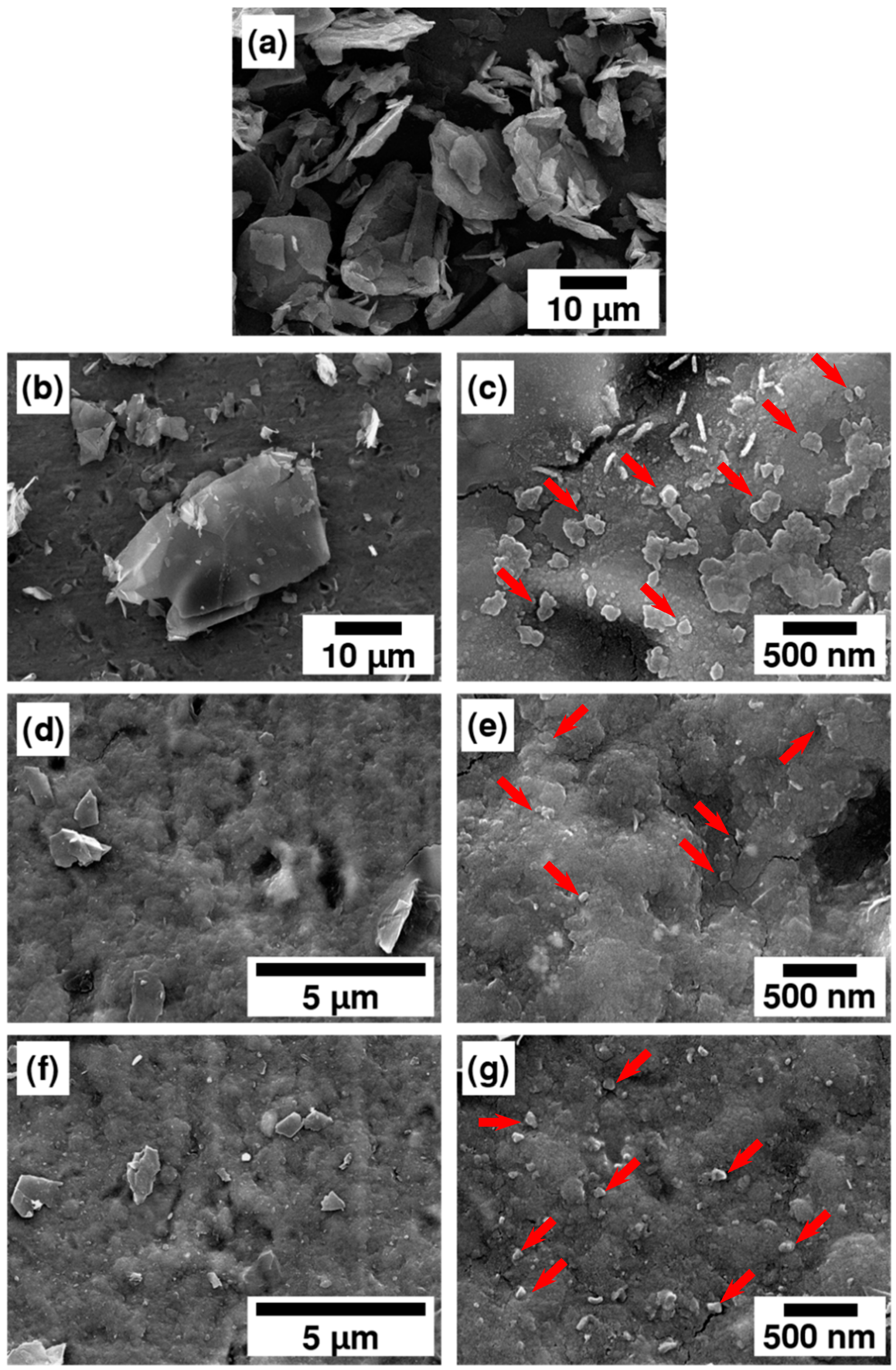
Figure 5.
(a) High-resolution transmission electron micropscopy (HR-TEM) image of the deposited film with scan speed 1.2 mm/min; (b) Fast Fourier transform (FFT) of image (a); (c) Histogram plot of the area surrounded by the yellow rectangular in (a); (d) Magnified HR-TEM of the area surrounded by the yellow rectangular in (a) (in the top right, FFT of image (d) was inserted).


Figure 6.
X-ray diffraction (XRD) of the graphite powder, SUS304 substrate, and deposited films at different scan speeds.
Figure 6.
X-ray diffraction (XRD) of the graphite powder, SUS304 substrate, and deposited films at different scan speeds.

Figure 7.
Raman spectroscopy of (a) the graphite powder and deposited films at different scan speeds on larger size particles with less fragmentation and (b) graphite powder and deposited films at different scan speeds on the more fragmented particles.
Figure 7.
Raman spectroscopy of (a) the graphite powder and deposited films at different scan speeds on larger size particles with less fragmentation and (b) graphite powder and deposited films at different scan speeds on the more fragmented particles.

Figure 8.
(a–c) Cyclic voltammetry (CV) curves of 0.03 mol of H3PO4 gel electrolyte with different scan speeds; (d) Calculated specific areal capacitance from CV curves.
Figure 8.
(a–c) Cyclic voltammetry (CV) curves of 0.03 mol of H3PO4 gel electrolyte with different scan speeds; (d) Calculated specific areal capacitance from CV curves.

Figure 9.
CV curves of (a) 0.06 and (b) 0.09 mol of H3PO4 gel electrolyte with a 1.2 mm/min scan speed electrode; (c) The calculated areal capacitance for 0.06 and 0.09 mol of H3PO4 gel electrolyte with a 1.2 mm/min scan speed electrode.
Figure 9.
CV curves of (a) 0.06 and (b) 0.09 mol of H3PO4 gel electrolyte with a 1.2 mm/min scan speed electrode; (c) The calculated areal capacitance for 0.06 and 0.09 mol of H3PO4 gel electrolyte with a 1.2 mm/min scan speed electrode.

Figure 10.
(a–c) Galvanostatic Charge–discharge curves of 0.03 mol of H3PO4 gel electrolyte with different scan speeds; (d) Calculated specific areal capacitance from Charge–discharge curves.
Figure 10.
(a–c) Galvanostatic Charge–discharge curves of 0.03 mol of H3PO4 gel electrolyte with different scan speeds; (d) Calculated specific areal capacitance from Charge–discharge curves.

Figure 11.
Galvanostatic Charge–discharge curves of (a) 0.06 and (b) 0.09 mol of H3PO4 gel electrolyte with a 1.2 mm/min scan speed electrode; (c) The calculated areal capacitance for 0.06 and 0.09 mol of H3PO4 gel electrolyte with a 1.2 mm/min scan speed electrode.
Figure 11.
Galvanostatic Charge–discharge curves of (a) 0.06 and (b) 0.09 mol of H3PO4 gel electrolyte with a 1.2 mm/min scan speed electrode; (c) The calculated areal capacitance for 0.06 and 0.09 mol of H3PO4 gel electrolyte with a 1.2 mm/min scan speed electrode.


Figure 12.
Nyquist plots of (a) 0.03 mol of H3PO4 gel electrolyte with different scan speeds and (b) 0.03, 0.06 and 0.09 mol of H3PO4 gel electrolyte with a 1.2 mm/min scan speed electrode.
Figure 12.
Nyquist plots of (a) 0.03 mol of H3PO4 gel electrolyte with different scan speeds and (b) 0.03, 0.06 and 0.09 mol of H3PO4 gel electrolyte with a 1.2 mm/min scan speed electrode.

Figure 13.
Charge–discharge stability over 5000 cycles for a 1.2 mm/min scan speed and 0.09 mol of H3PO4–PVA at a current of 0.06 mA.
Figure 13.
Charge–discharge stability over 5000 cycles for a 1.2 mm/min scan speed and 0.09 mol of H3PO4–PVA at a current of 0.06 mA.


Table 1.
Process parameters for graphite deposition on the stainless-steel substrate.
| Parameter | Value |
|---|---|
| Compressor pressure (MPa) | 0.2 |
| Chamber pressure (MPa) | 0.036–0.04 |
| Scan speed (mm/min) | 0.4, 0.8, and 1.2 |
| Distance between substrate and nozzle (mm) | 5 |
| Deposition shape | 2 × 5 cm2 |
| Substrate material | Stainless-steel |
Table 2.
Thickness and mass values of the deposited films with different scan speeds.
| Scan Speed (mm/min) | Thickness (μm) | Mass (mg/cm2) |
|---|---|---|
| 0.4 | 2.53 | 0.3 |
| 0.8 | 1.54 | 0.17 |
| 1.2 | 0.85 | 0.101 |
Table 3.
D, G, and 2D peaks and ID/IG for the graphite powder and deposited films.
| Sample | Large Size & Less Fragmented Particles | Fragmented Particles | ||||||
|---|---|---|---|---|---|---|---|---|
| D Peak (cm−1) | G Peak (cm−1) | 2D Peak (cm−1) | ID/IG | D Peak (cm−1) | G Peak (cm−1) | 2D Peak (cm−1) | ID/IG | |
| Powder | 1352.4 | 1582.1 | 2720.8 | 0.269 | 1352.4 | 1582.1 | 2720.8 | 0.269 |
| 0.4 mm/min | 1352.4 | 1586 | 2718 | 0.647 | 1352.4 | 1598.5 | 2698 | 1.054 |
| 0.8 mm/min | 1352.4 | 1592 | 2708 | 0.970 | 1352.4 | 1597 | 2698 | 1.064 |
| 1.2 mm/min | 1352.4 | 1596 | 2699 | 1.009 | 1350.8 | 1595 | 2698 | 1.069 |
© 2018 by the authors. Licensee MDPI, Basel, Switzerland. This article is an open access article distributed under the terms and conditions of the Creative Commons Attribution (CC BY) license (http://creativecommons.org/licenses/by/4.0/).
Share and Cite
MDPI and ACS Style
Mohammed, M.M.M.; Chun, D.-M. Electrochemical Performance of Few-Layer Graphene Nano-Flake Supercapacitors Prepared by the Vacuum Kinetic Spray Method. Coatings 2018, 8, 302. https://doi.org/10.3390/coatings8090302
AMA Style
Mohammed MMM, Chun D-M. Electrochemical Performance of Few-Layer Graphene Nano-Flake Supercapacitors Prepared by the Vacuum Kinetic Spray Method. Coatings. 2018; 8(9):302. https://doi.org/10.3390/coatings8090302
Chicago/Turabian StyleMohammed, Mohaned Mohammed Mahmoud, and Doo-Man Chun. 2018. "Electrochemical Performance of Few-Layer Graphene Nano-Flake Supercapacitors Prepared by the Vacuum Kinetic Spray Method" Coatings 8, no. 9: 302. https://doi.org/10.3390/coatings8090302
Note that from the first issue of 2016, this journal uses article numbers instead of page numbers. See further details here.