Facile Solution Spin-Coating SnO2 Thin Film Covering Cracks of TiO2 Hole Blocking Layer for Perovskite Solar Cells

Abstract
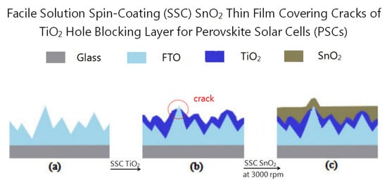
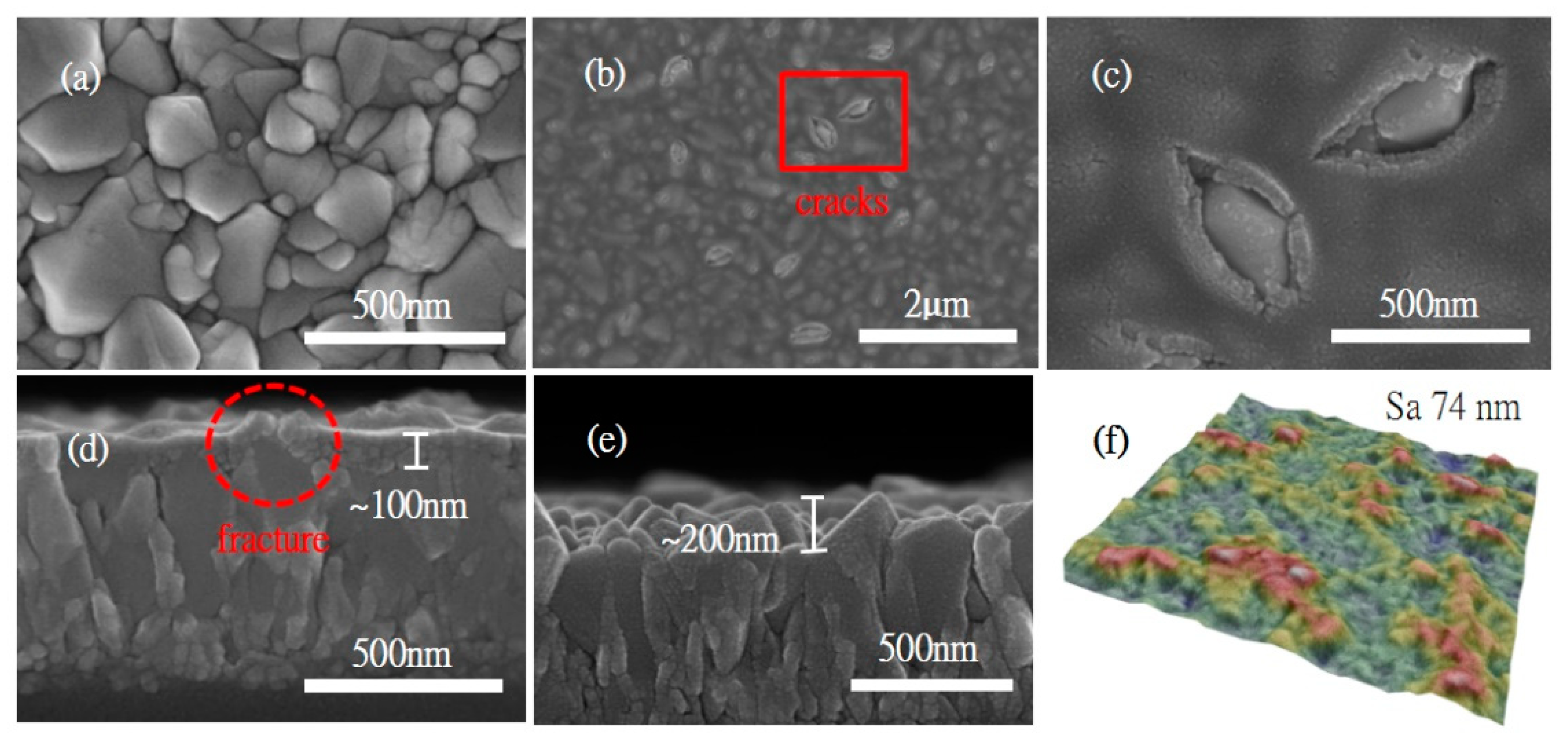
:
1. Introduction
2. Materials and Methods
2.1. Materials
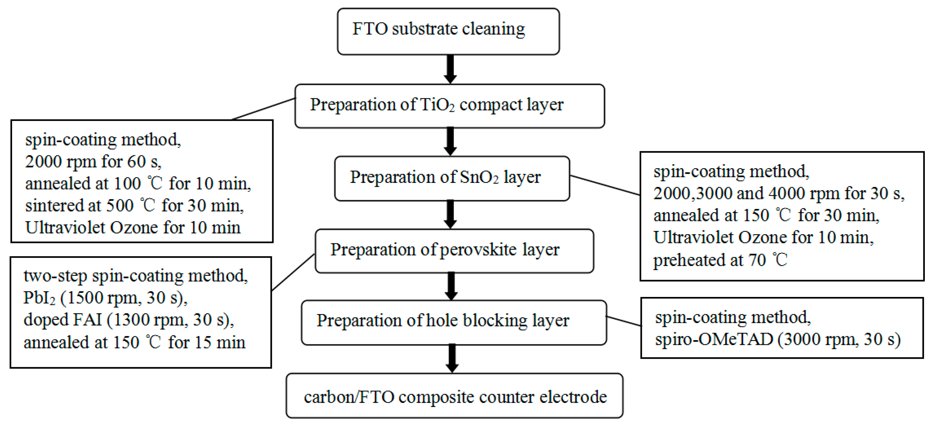
2.2. Device Fabrication
2.3. Characterization
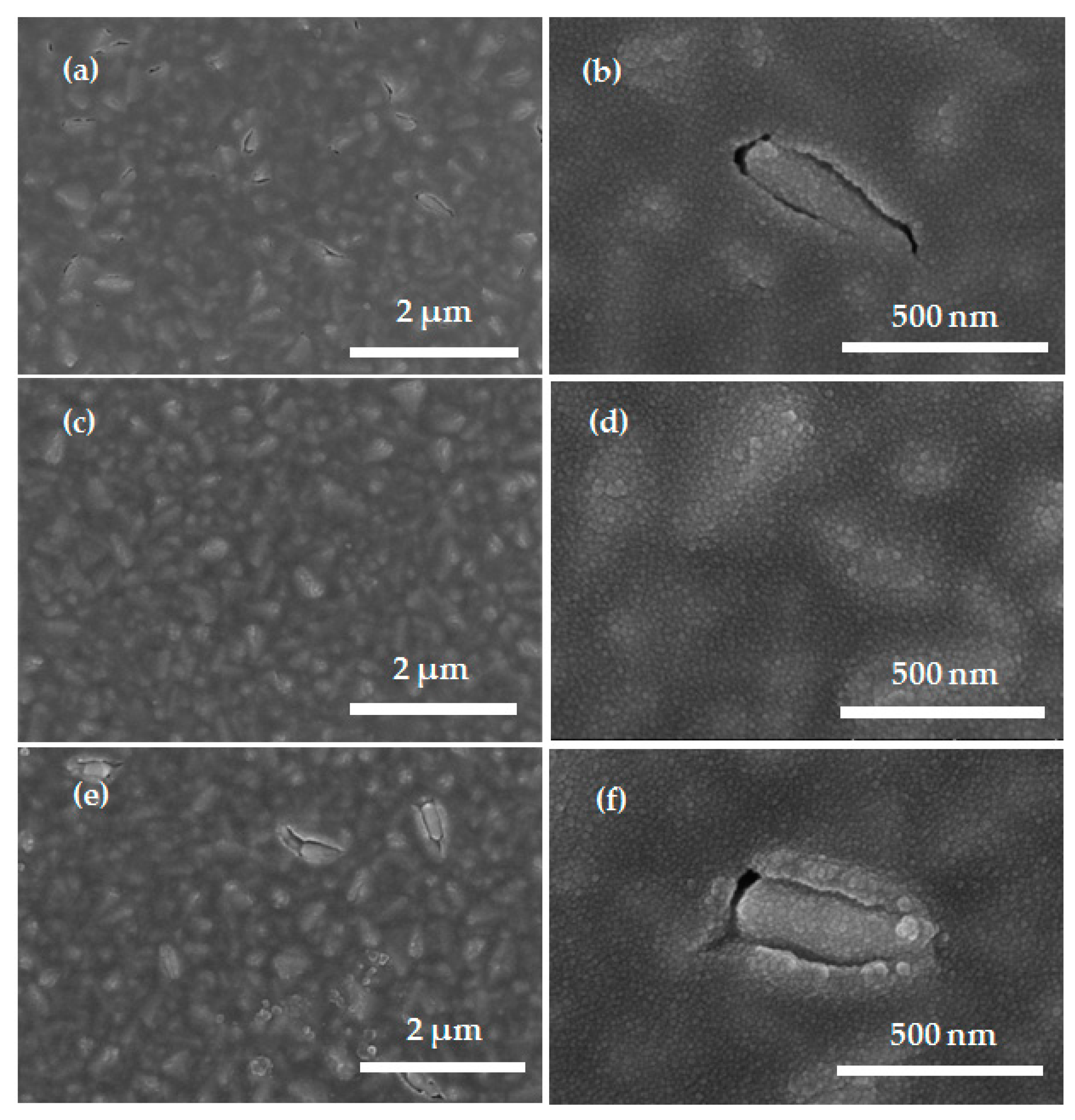
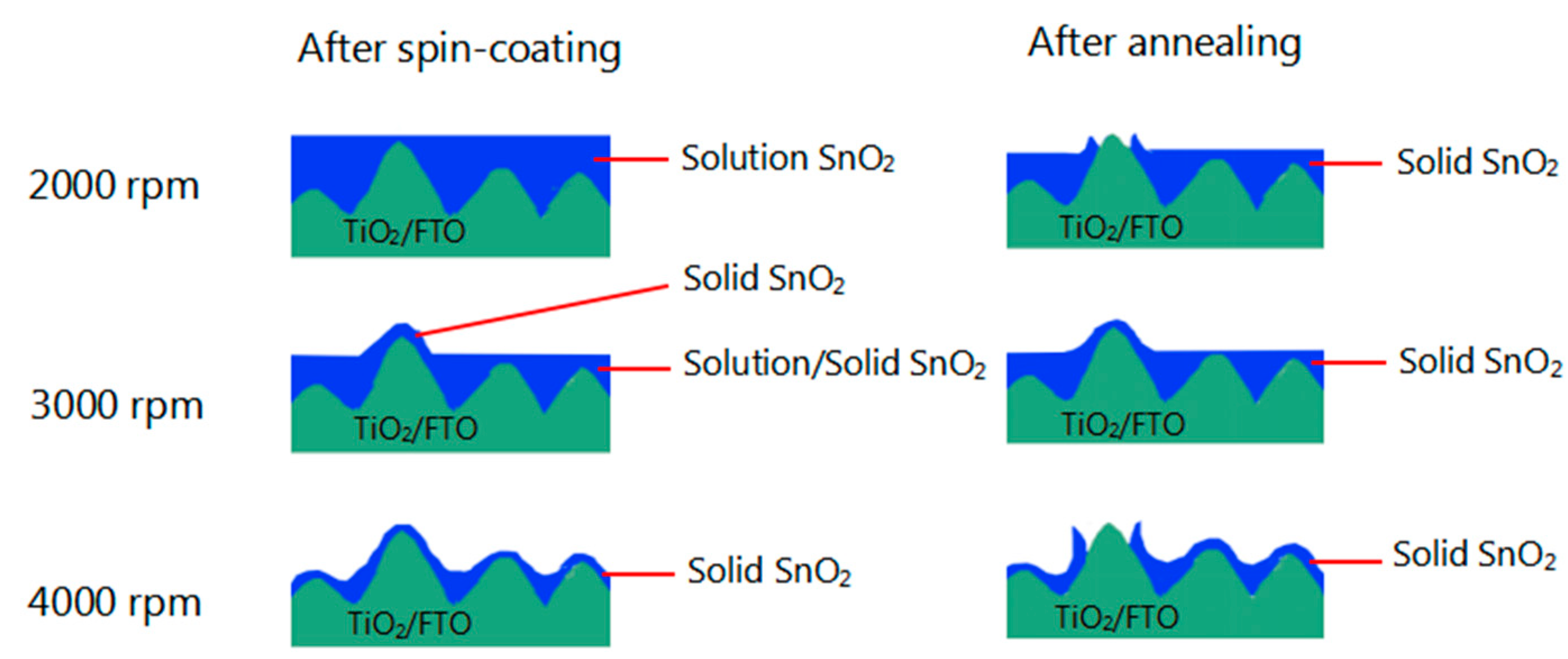
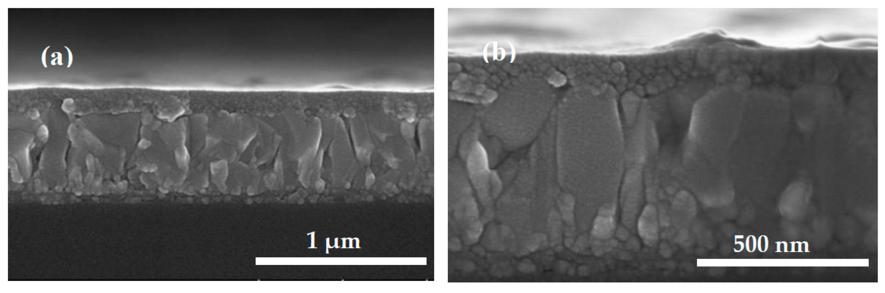
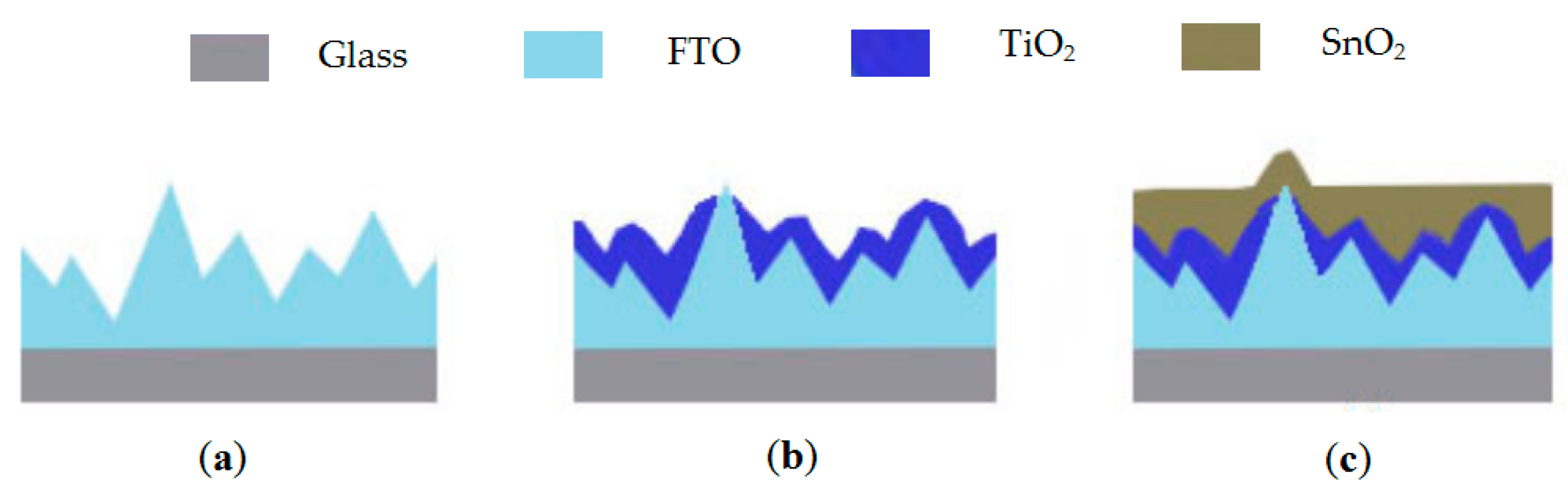
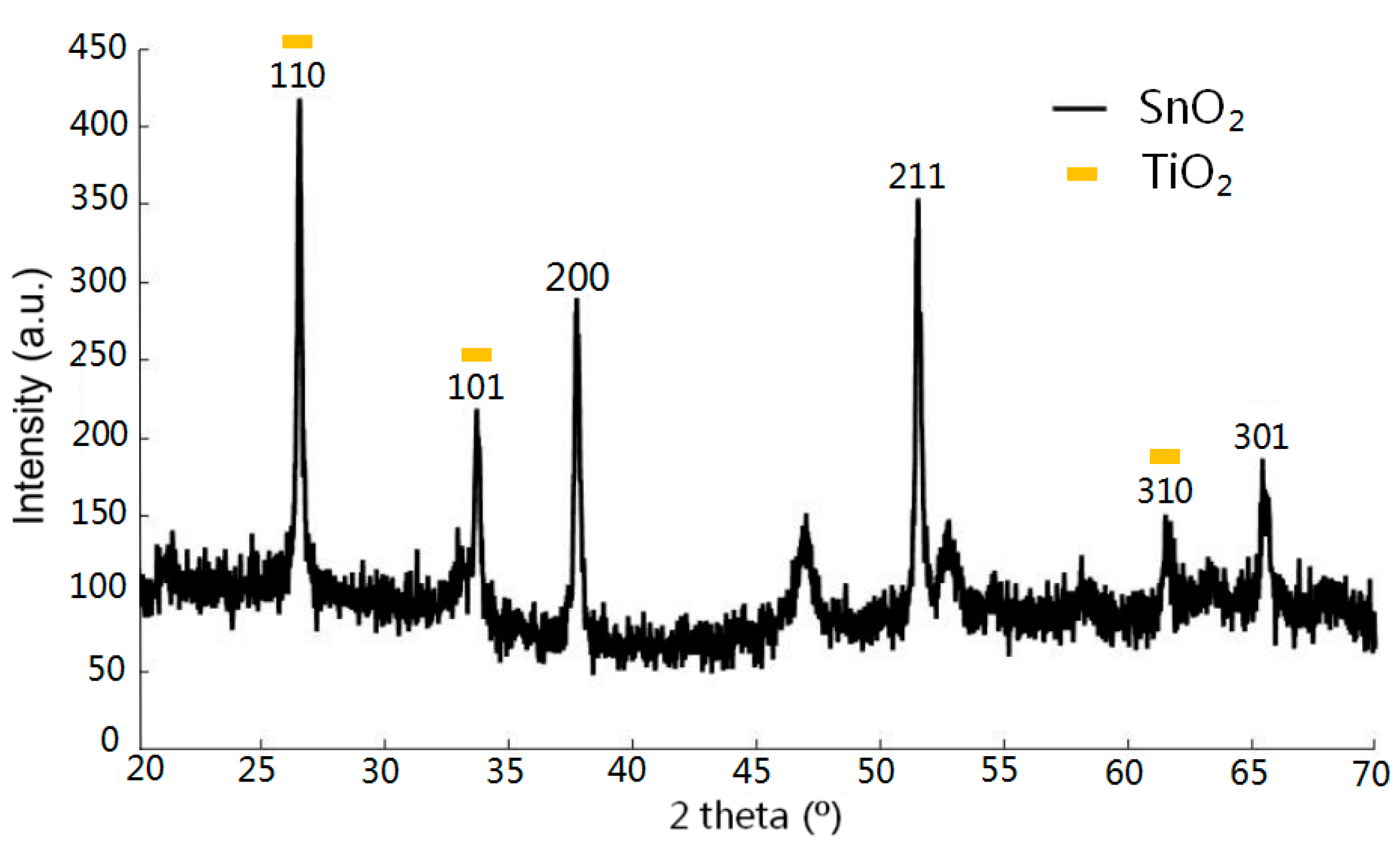
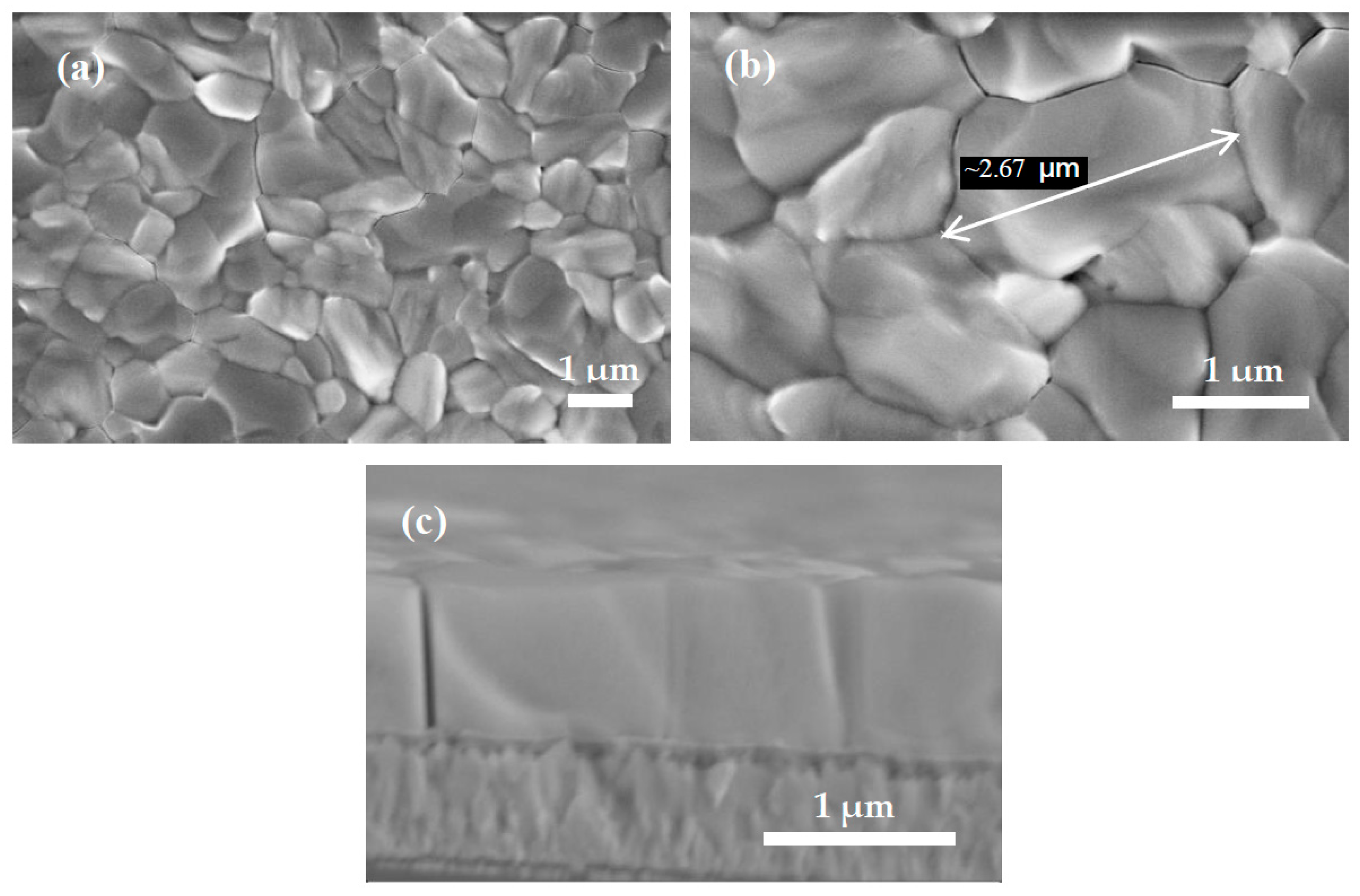
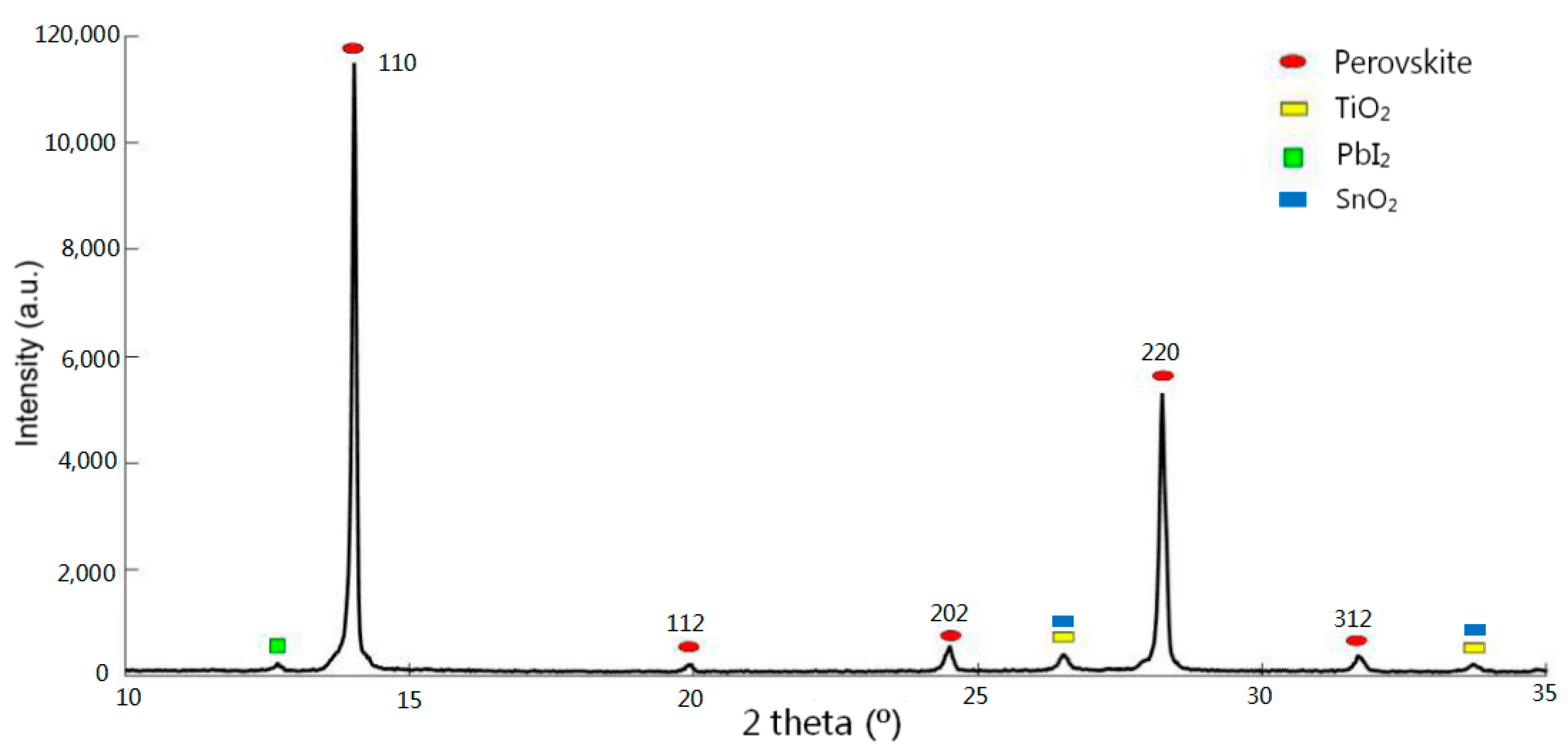
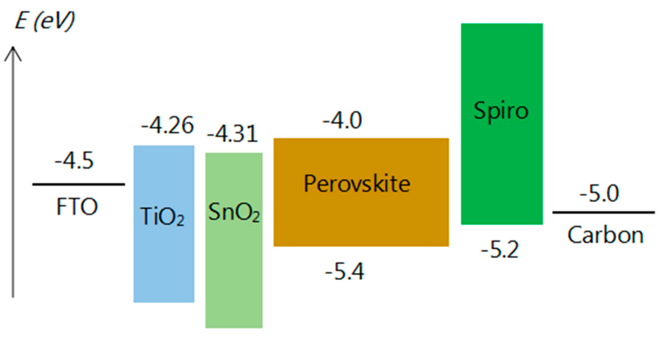
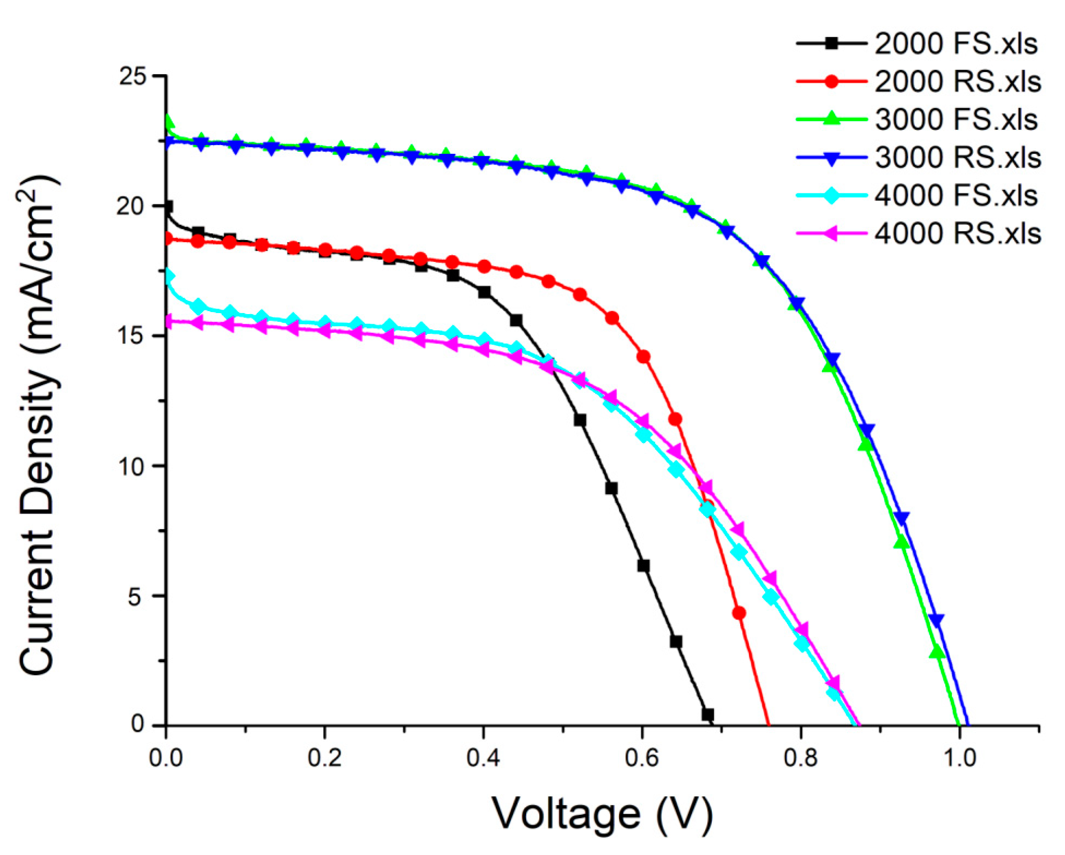
3. Results and Discussion
4. Conclusions
Author Contributions
Funding
Conflicts of Interest
References
- Snaith, H.J. Perovskites: The emergence of a new Era for low-cost, high-efficiency solar cells. J. Phys. Chem. Lett. 2013, 4, 3623–3630. [Google Scholar] [CrossRef]
- Park, N.G. Organometal perovskite light absorbers toward a 20% efficiency low-cost solid-state mesoscopic solar cell. J. Phys. Chem. Lett. 2013, 4, 2423–2429. [Google Scholar] [CrossRef]
- Green, M.A.; Ho-Baillie, A.; Snaith, H.J. The emergence of perovskite solar cells. Nat. Photonics 2014, 8, 506–514. [Google Scholar] [CrossRef]
- Grätzel, M. The light and shade of perovskite solar cells. Nat. Mater. 2014, 13, 838–842. [Google Scholar] [CrossRef] [PubMed]
- Abdi-Jalebi, M.; Pazoki, M.; Philippe, B.; Dar, M.I.; Alsari, M.; Sadhanala, A.; Diyitini, G.; Imani, R.; Lilliu, S.; Kullgren, J.; et al. Dedoping of lead halide perovskites incorporating monovalent cations. ACS Nano 2018, 12, 7301–7311. [Google Scholar] [CrossRef] [PubMed]
- Alsari, M.; Bikondoa, O.; Bishop, J.; Abdi-Jalebi, M.; Ozer, L.Y.; Hampton, M.; Thompson, P.; Horantner, M.T.; Mahesh, S.; Greenland, C.; et al. In situ simultaneous photovoltaic and structural evolution of perovskite solar cells during film formation. Energy Environ. Sci. 2018, 11, 383–393. [Google Scholar] [CrossRef] [Green Version]
- Alsari, M.; Pearson, A.J.; Wang, J.T.W.; Wang, Z.P.; Montisci, A.; Greenham, N.C.; Snaith, H.J.; Lilliu, S.; Friend, H. Degradation kinetics of inverted perovskite solar cells. Sci. Rep. 2018, 8, 5977. [Google Scholar] [CrossRef] [PubMed]
- Liu, Z.Y.; Sun, B.; Liu, X.Y.; Han, J.H.; Ye, H.B.; Tu, Y.X.; Chen, C.; Shi, T.L.; Lang, Z.R.; Liao, G.L. 15% efficient carbon based planar-heterojunction perovskite solar cells using TiO2/SnO2 bilayer as electron transport layer. J. Mater. Chem. A 2018, 6, 7409–7419. [Google Scholar] [CrossRef]
- Ren, Z.Q.; Wang, N.; Zhu, M.H.; Li, X.; Qi, J.Y. A NH4F interface passivation strategy to produce air-processed high-performance planar perovskite solar cells. Electrochim. Acta 2018, 282, 653–661. [Google Scholar] [CrossRef]
- Li, X.; Yang, J.Y.; Jiang, Q.H.; Lai, H.; Li, S.P.; Xin, J.W.; Chu, W.J.; Hou, J.D. Low-temperature solution-processed znse electron transport layer for efficient planar perovskite solar cells with negligible hysteresis and improved photostability. ACS Nano 2018, 12, 5605–5614. [Google Scholar] [CrossRef] [PubMed]
- Ma, J.J.; Yang, G.; Qin, M.C.; Zheng, X.L.; Lei, H.W.; Chen, C.; Chen, Z.L.; Guo, Y.X.; Han, H.W.; Zhao, X.Z.; et al. MgO nanoparticle modified anode for highly efficient SnO2-based planar perovskite solar cells. Adv. Sci. 2017, 4, 1700031. [Google Scholar] [CrossRef] [PubMed]
- Wu, Y.Z.; Yang, X.D.; Chen, H.; Zhang, K.; Qin, C.J.; Liu, J.; Peng, W.Q.; Islam, A.; Bi, E.B.; Ye, F.; et al. Highly compact TiO2 layer for efficient hole-blocking in perovskite solar cells. Appl. Phys. Express 2014, 7, 052301. [Google Scholar] [CrossRef]
- Liu, Y.; Peng, Q.; Zhou, Z.P.; Yang, G. Effects of substrate temperature on properties of transparent conductive Ta-doped TiO2 films deposited by radio-frequency magnetron sputtering. Chin. Phys. Lett. 2018, 35, 048101. [Google Scholar] [CrossRef]
- Duong, T.T.; Kim, Y.J.; Eom, J.H.; Choi, J.S.; Le, A.T.; Yoon, S.G. Enhancement of solar cell efficiency using perovskite dyes deposited via a two-step process. RSC Adv. 2015, 5, 33515–33523. [Google Scholar] [CrossRef]
- Choi, J.; Song, S.; Horantner, M.T.; Snaith, H.J.; Park, T. Well-defined nanostructured, single-crystalline TiO2 electron transport layer for efficient planar perovskite solar cells. ACS Nano 2016, 10, 6029–6036. [Google Scholar] [CrossRef] [PubMed]
- Zhang, N.; Guo, Y.; Yin, X.; He, M.; Zou, X. Spongy carbon film deposited on a separated substrate as counter electrode for perovskite-based solar cell. Mater. Lett. 2016, 182, 248–252. [Google Scholar] [CrossRef]
- Mei, A.; Li, X.; Liu, L.; Ku, Z.; Liu, T.; Rong, Y.G.; Xu, M.; Hu, M.; Chen, J.; Yang, Y.; et al. A hole-conductor-free, fully printable mesoscopic perovskite solar cell with high stability. Science 2014, 345, 295–298. [Google Scholar] [CrossRef] [PubMed]
- Habisreutinger, S.N.; Leijtens, T.; Eperon, G.E.; Stranks, S.D.; Nicholas, R.J.; Snaith, H.J. Carbon nanotube/polymer composites as a highly stable hole collection layer in perovskite solar cells. Nano Lett. 2014, 14, 5561–5568. [Google Scholar] [CrossRef] [PubMed]
- Ling, T.; Zou, X.P.; Cheng, J.; Bai, X.; Ren, H.Y.; Chen, D. Modified sequential deposition route through localized-liquid-liquid-diffusion for improved perovskite multi-crystalline thin films with micrometer-scaled grains for solar cells. Nanomaterials 2018, 8, 416. [Google Scholar] [CrossRef] [PubMed]
- Wu, C.C.; Huang, Z.R.; He, Y.H.; Luo, W.; Ting, H.K.; Li, T.Y.; Sun, W.H.; Zhang, Q.H.; Chen, Z.J.; Xiao, L.X. TiO2/SnOxCly double layer for highly efficient planar perovskite solar cells. Org. Electron. 2017, 50, 485–490. [Google Scholar] [CrossRef]
- Ke, W.J.; Fang, G.J.; Liu, Q.; Xiong, L.B.; Qin, P.L.; Tao, H.; Wang, J.; Lei, W.H.; Li, B.R.; Wan, J.W.; et al. Low-temperature solution-processed tin oxide as an alternative electron transporting layer for efficient perovskite solar cells. J. Am. Chem. Soc. 2015, 137, 6730–6733. [Google Scholar] [CrossRef] [PubMed]
- Song, J.X.; Zheng, E.Q.; Bian, J.; Wang, X.F.; Tian, W.J.; Sanehira, Y.; Miyasaka, T. Low-temperature SnO2-based electron selective contact for efficient and stable perovskite solar cells. J. Mater. Chem. A 2015, 3, 10837–10844. [Google Scholar] [CrossRef]
- Jiang, Q.; Zhang, L.Q.; Wang, H.L.; Yang, X.L.; Meng, J.H.; Liu, H.; Yin, Z.G.; Wu, J.L.; Zang, X.W.; You, J.B. Enhanced electron extraction using SnO2 for high-efficiency planar-structure HC(NH2)2PbI3-based perovskite solar cells. Nat. Energy 2017, 2, 16177. [Google Scholar] [CrossRef]
- Baena, J.P.C.; Steier, L.; Tress, W.; Saliba, M.; Neutzner, S.; Matsui, T.; Giordano, F.; Jacobsson, T.J.; Kandada, A.R.S.; Zakeeruddin, S.M.; et al. Highly efficient planar perovskite solar cells through band alignment engineering. Energy Environ. Sci. 2015, 8, 2928–2934. [Google Scholar] [CrossRef] [Green Version]
- Chen, J.Y.; Chueh, C.C.; Zhu, Z.L.; Chen, W.C.; Jen, A.K.Y. Low-temperature electrodeposited crystalline SnO2 as an efficient electron transporting layer for conventional perovskite solar cells. Sol. Energy Mater. Sol. Cells 2017, 164, 47–55. [Google Scholar] [CrossRef]
- Anaraki, E.H.; Kermanpur, A.; Steier, L.; Domanski, K.; Matsui, T.; Tress, W.; Saliba, M.; Abate, A.; Grätzel, M.; Hagfeldt, A.; et al. Highly efficient and stable planar perovskite solar cells by solution-processed tin oxide. Energy Environ. Sci. 2016, 9, 3128–3134. [Google Scholar] [CrossRef]
- Malviya, K.D.; Dotan, H.; Yoon, K.R.; Kim, I.D.; Rothschild, A. Rigorous substrate cleaning process for reproducible thin film hematite (alpha-Fe2O3) photoanodes. J. Mater. Res. 2016, 31, 1565–1573. [Google Scholar] [CrossRef]
- Huang, L.K.; Li, C.; Sun, X.X.; Xu, R.; Du, Y.Y.; Ni, J.; Cai, H.K.; Li, J.; Hu, Z.Y.; Zhang, J.J. Efficient and hysteresis-less pseudo-planar heterojunction perovskite solar cells fabricated by a facile and solution-saving one-step dip-coating method. Org. Electron. 2017, 40, 13–23. [Google Scholar] [CrossRef]
- Masood, M.T.; Weinberger, C.; Sarfraz, J.; Rosqvist, E.; Sanden, S.; Sandberg, O.J.; Vivo, P.; Hashmi, G.; Lund, P.D.; Osterbacka, R.; et al. Impact of film thickness of ultrathin dip-coated compact TiO2 layers on the performance of mesoscopic perovskite solar cells. ACS Appl. Mater. Interfaces 2017, 9, 17906–17913. [Google Scholar] [CrossRef] [PubMed]
- Du, Q.G.; Shen, G.S.; John, S. Light-trapping in perovskite solar cells. AIP Adv. 2016, 6, 065002. [Google Scholar] [CrossRef]
- Iftiquar, S.M.; Yi, J.S. Numerical simulation and light trapping in perovskite solar cell. J. Photonics Energy 2016, 6, 025507. [Google Scholar] [CrossRef]
- Peer, A.; Biswas, R.; Park, J.M.; Shinar, R.; Shinar, J. Light management in perovskite solar cells and organic LEDs with microlens arrays. Opt. Express 2017, 25, 10704–10709. [Google Scholar] [CrossRef] [PubMed]
- Bhattacharya, J.; Peer, A.; Joshi, P.H.; Biswas, R.; Dalal, V.L. Blue photon management by inhouse grown ZnO:Al cathode for enhanced photostability in polymer solar cells. Sol. Energy Mater. Sol. Cells 2018, 179, 95–101. [Google Scholar] [CrossRef]
- Lee, Y.H.; Paek, S.; Cho, K.T.; Oveisi, E.; Gao, P.; Lee, S.; Park, J.S.; Zhang, Y.; Humphry-Baker, R.; Asiri, A.M.; et al. Enhanced charge collection with passivation of the tin oxide layer in planar perovskite solar cells. J. Mater. Chem. A 2017, 5, 12729–12734. [Google Scholar] [CrossRef]


| Devices | Na | Jscb (mA/cm2) | Vocc (V) | FF d | PCE e (%) |
|---|---|---|---|---|---|
| R1 | 1 | 13.13 | 0.86 | 41.09 | 4.63 |
| R2 | 2 | 18.26 | 0.97 | 54.70 | 9.66 |
| RSSC a (rpm) | Jscb (mA/cm2) | Vocc (V) | FF d | PCE e (%) |
|---|---|---|---|---|
| 2000 | 18.74 | 0.76 | 61.95 | 8.81 |
| 3000 | 22.48 | 1.01 | 59.51 | 13.52 |
| 4000 | 15.56 | 0.87 | 52.22 | 7.10 |
© 2018 by the authors. Licensee MDPI, Basel, Switzerland. This article is an open access article distributed under the terms and conditions of the Creative Commons Attribution (CC BY) license (http://creativecommons.org/licenses/by/4.0/).
Share and Cite
Ren, H.; Zou, X.; Cheng, J.; Ling, T.; Bai, X.; Chen, D. Facile Solution Spin-Coating SnO2 Thin Film Covering Cracks of TiO2 Hole Blocking Layer for Perovskite Solar Cells. Coatings 2018, 8, 314. https://doi.org/10.3390/coatings8090314
Ren H, Zou X, Cheng J, Ling T, Bai X, Chen D. Facile Solution Spin-Coating SnO2 Thin Film Covering Cracks of TiO2 Hole Blocking Layer for Perovskite Solar Cells. Coatings. 2018; 8(9):314. https://doi.org/10.3390/coatings8090314
Chicago/Turabian StyleRen, Haiyan, Xiaoping Zou, Jin Cheng, Tao Ling, Xiao Bai, and Dan Chen. 2018. "Facile Solution Spin-Coating SnO2 Thin Film Covering Cracks of TiO2 Hole Blocking Layer for Perovskite Solar Cells" Coatings 8, no. 9: 314. https://doi.org/10.3390/coatings8090314